ICGOO在线商城 > 电路保护 > TVS - 混合技术 > SP724AHTG
 Datasheet下载
- 型号: SP724AHTG
- 制造商: Littelfuse
- 库位|库存: xxxx|xxxx
- 要求:
| 数量阶梯 | 香港交货 | 国内含税 |
| +xxxx | $xxxx | ¥xxxx |
查看当月历史价格
查看今年历史价格
SP724AHTG产品简介:
ICGOO电子元器件商城为您提供SP724AHTG由Littelfuse设计生产,在icgoo商城现货销售,并且可以通过原厂、代理商等渠道进行代购。 SP724AHTG价格参考¥询价-¥询价。LittelfuseSP724AHTG封装/规格:TVS - 混合技术, 。您可以下载SP724AHTG参考资料、Datasheet数据手册功能说明书,资料中有SP724AHTG 详细功能的应用电路图电压和使用方法及教程。
Littelfuse Inc.的SP724AHTG是一款TVS(瞬态电压抑制器)混合技术器件,主要用于保护敏感电子设备免受静电放电(ESD)、电快速瞬变脉冲群(EFT)和雷击感应浪涌等瞬态过电压事件的损害。其应用场景广泛,特别适用于消费电子、通信设备、工业控制、汽车电子等领域。

1. 消费电子产品:如智能手机、平板电脑、笔记本电脑等。这些设备中的接口(如USB、HDMI、耳机插孔等)容易受到外部瞬态电压的影响,SP724AHTG可以有效保护内部电路不受损坏,确保设备的可靠性和使用寿命。

2. 通信设备:包括路由器、交换机、调制解调器等网络设备。这些设备通常需要通过以太网口、光纤接口等与外界连接,容易受到雷击或电源波动的影响。SP724AHTG能够提供强大的瞬态电压抑制能力,保护通信链路的稳定性和数据传输的安全性。

3. 工业控制系统:例如PLC(可编程逻辑控制器)、传感器、执行器等。工业环境中的电气干扰较为严重,尤其是电机启动、开关操作等产生的瞬态电压可能会对控制系统造成损害。SP724AHTG可以有效防止这种瞬态电压对系统的影响,保障工业生产的连续性和安全性。

4. 汽车电子:如车载信息娱乐系统、导航系统、倒车雷达等。汽车在行驶过程中会遇到各种复杂的电磁环境,尤其是在雷雨天气或经过高压线附近时,瞬态电压可能会影响车载电子系统的正常工作。SP724AHTG能够在这些情况下为汽车电子提供可靠的保护,确保行车安全。

5. 医疗设备:如心电图机、超声波仪等精密仪器。这些设备对瞬态电压非常敏感,任何微小的电压波动都可能导致测量不准确或设备故障。SP724AHTG可以有效保护这些设备的内部电路,确保医疗诊断和治疗的准确性。

总之,SP724AHTG凭借其卓越的瞬态电压抑制性能,广泛应用于各种需要高可靠性保护的电子设备中,确保设备在复杂电磁环境中稳定运行。
| 参数 | 数值 |
| 产品目录 | |
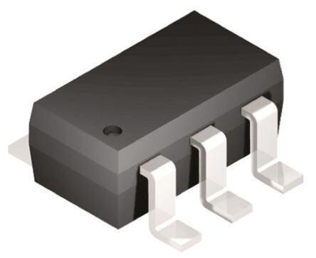
| 描述 | TVS ARRAY ESD 4CH 20V SOT-23ESD 抑制器 20V 2.2A 4 CHANNEL |
| 产品分类 | TVS - 其它复合ESD 抑制器 |
| 品牌 | Littelfuse |
| 产品手册 | |
| 产品图片 |
|
| rohs | 符合RoHS无铅 / 符合限制有害物质指令(RoHS)规范要求 |
| 产品系列 | Littelfuse SP724AHTG- |
| 数据手册 | |
| 产品型号 | SP724AHTG |
| 产品培训模块 | http://www.digikey.cn/PTM/IndividualPTM.page?site=cn&lang=zhs&ptm=25590 |
| 产品目录绘图 |
|
| 产品目录页面 | |
| 产品种类 | ESD 抑制器 |
| 供应商器件封装 | SOT-23-6 |
| 其它名称 | F2863CT |
| 击穿电压 | 20 V |
| 功率(W) | - |
| 包装 | 剪切带 (CT) |
| 商标 | Littelfuse |
| 安装风格 | SMD/SMT |
| 封装 | Reel |
| 封装/外壳 | SOT-23-6 |
| 封装/箱体 | SOT-23-6 |
| 尺寸 | 1.75 mm W x 3 mm L x 1.3 mm H |
| 峰值浪涌电流 | 3 A |
| 工作温度范围 | - 40 C to + 105 C |
| 工作电压 | 1 V to 20 V |
| 工厂包装数量 | 3000 |
| 应用 | 通用 |
| 技术 | 混合技术 |
| 最大工作温度 | + 105 C |
| 最小工作温度 | - 40 C |
| 极性 | Bidirectional |
| 标准包装 | 1 |
| 电压-工作 | 20V |
| 电压-箝位 | - |
| 电容 | 3 pF |
| 电路数 | 4 |
| 端接类型 | SMD/SMT |
| 系列 | SP724 SPA |
| 通道 | 4 Channels |


- 商务部:美国ITC正式对集成电路等产品启动337调查
- 曝三星4nm工艺存在良率问题 高通将骁龙8 Gen1或转产台积电
- 太阳诱电将投资9.5亿元在常州建新厂生产MLCC 预计2023年完工
- 英特尔发布欧洲新工厂建设计划 深化IDM 2.0 战略
- 台积电先进制程称霸业界 有大客户加持明年业绩稳了
- 达到5530亿美元!SIA预计今年全球半导体销售额将创下新高
- 英特尔拟将自动驾驶子公司Mobileye上市 估值或超500亿美元
- 三星加码芯片和SET,合并消费电子和移动部门,撤换高东真等 CEO
- 三星电子宣布重大人事变动 还合并消费电子和移动部门
- 海关总署:前11个月进口集成电路产品价值2.52万亿元 增长14.8%


PDF Datasheet 数据手册内容提取
TVS Diode Arrays (SPA® Diodes) General Purpose ESD Protection - SP724 Series SP724 Series 3pF 8kV Diode Array RoHS Pb GREEN Description The SP724 is a quad array of transient voltage clamping circuits designed to suppress ESD and other transient over- voltage events. The SP724 is used to help protect sensitive digital or analog input circuits on data, signal, or control lines operating on power supplies up to 20VDC. The SP724 is comprised of bipolar SCR/diode structures to protect up to four independent lines by clamping transients of either polarity to the power supply rails. The SP724 offers very low leakage (1nA Typical) and low input capacitance (3pF Typical). Additionally, the SP724 is rated to withstand the IEC 61000-4-2 ESD specification for both contact and air discharge methods to level 4. Pinout The SP724 is connected to the sensitive input line and its associated power supply lines. Clamping action occurs I/O V+ I/O during the transient pulse, turning on the diode and fast 6 5 4 triggering SCR structures when the voltage on the input SP724 line exceeds one V threshold above the V+ supply (or one BE (SOT-23) V threshold below the V- supply). Therefore, the SP724P BE TOP VIEW operation is unaffected by poor power supply regulation or voltage fluctuations within its operating range. 1 2 3 I/O V– I/O Features • An Array of 4 SCR/Diode Pairs in 6-Lead SOT-23 Functional Block Diagram • ESD Capability per HBM Standards - IEC 61000-4-2, Direct Discharge ..........8kV (Level 4) - IEC 61000-4-2, Air Discharge ...............15kV (Level 4) - MIL STD 3015.7 ................................................>8kV • Input Protection for Applications with Power Supplies Up to +20V (Single-Ended Voltage), and ±10V (Differential Voltage) • Peak Current Capability - IEC 61000-4-5 (8/20µs) .......................................±3A - Single Pulse, 100µs Pulse Width .....................±2.2A • Low Input Leakage ..........................................1nA Typical Notes: • Low Input Capacitance .....................................3pF Typical 1. The design of the SP724 SCR/Diode ESD Protection Arrays are covered by Littelfuse • Operating Temperature Range....................-40ºC to 105ºC patent 4567500. 2. The full ESD capability of the SP724 is achieved when wired in a circuit that includes connection to both the V+ and V- pins. When handling individual devices, follow proper procedures for electrostatic discharge. Applications • Microprocessor/Logic • Analog Device Input Input Protection Protection • Data Bus Protection • Voltage Clamp Additional Information Life Support Note: Not Intended for Use in Life Support or Life Saving Applications The products shown herein are not designed for use in life sustaining or life saving applications unless otherwise expressly indicated. Resources Samples © 2017 Littelfuse, Inc. Specifications are subject to change without notice. Revised: 05/12/17
TVS Diode Arrays (SPA® Diodes) General Purpose ESD Protection - SP724 Series Absolute Maximum Ratings Thermal Information Parameter Rating Units Parameter Rating Units Continuous Supply Voltage, (V+) - (V-) +20 V Thermal Resistance (Typical, Note 3) θJA oC/W Forward Peak Current, I to V , GND SOT Package 220 oC/W IN CC ±2.2, 100µs A (Refer to Figure 5) Maximum Storage Temperature Range -65 to 150 oC CAUTION: Stresses above those listed in “Absolute Maximum Ratings” may cause Maximum Junction Temperature 150 oC permanent damage to the device. This is a stress only rating and operation of the device Maximum Lead Temperature at these or any other conditions above those indicated in the operational sections of this 260 oC specification is not implied. (Soldering 20-40s) (SOT - Lead Tips Only) Note: Note: 3. θ is measured with the component mounted on an evaluation PC board in free air. ESD Ratings and Capability - See Figure 1, Table 1 JA Electrical Characteristics T = -40oC to 105oC, V = 0.5V , Unless Otherwise Specified A IN CC Parameter Symbol Test Conditions Min Typ Max Units Operating Voltage Range, V 1 - 20 V V = [(V+) - (V-)] (Notes 4, 5) SUPPLY SUPPLY Forward Voltage Drop Forward Voltage Drop IN to V- V I = 1A (Peak Pulse) - 2 - V FWDL IN IN to V+ V - 2 - V FWDH Input Leakage Current I -10 1 10 nA IN Quiescent Supply Current I V+ = 20V, V- = GND - - 100 nA QUIESCENT Equivalent SCR ON Threshold (Note 6) - 1.1 - V Equivalent SCR ON Resistance V /I (Note 6) - 1.0 - Ω FWD FWD Input Capacitance C - 3 - pF IN Notes: 4. In automotive and other battery charging systems, the SP724 power supply lines should be externally protected for load dump and reverse battery. When the V+ and V- Pins are connected to the same supply voltage source as the device or control line under protection, a current limiting resistor should be connected in series between the external supply and the SP724 supply pins to limit reverse battery current to within the rated maximum limits. 5. Bypass capacitors of typically 0.01µF or larger should be connected closely between the V+ and V- Pins for all applications. 6. Refer to the Figure 3 graph for definitions of equivalent “SCR ON Threshold” and “SCR ON Resistance”. These characteristics are given here for information to determine peak current and dissipation under EOS conditions. Typical Application of the SP724 Application as an Input Clamp for Over-voltage, Greater than 1V BE Above V+ or less than -1V below V-) BE © 2017 Littelfuse, Inc. Specifications are subject to change without notice. Revised: 05/12/17
TVS Diode Arrays (SPA® Diodes) General Purpose ESD Protection - SP724 Series ESD Capability ESD rating is dependent on the defined test standard. The Figure 1: Electrostatic Discharge Test evaluation results for various test standards and methods based on Figure 1 are shown in Table 1.3 The SP724 has a Level 4 rating when tested to the IEC 61000-4-2 Human Body Model (HBM) standard and connected in a circuit in which the V+ and V- pins have a return path to ground. Level 4 specifies a required capability greater than 8kV for direct discharge and greater than 15kV for air discharge. The “Modified” MIL-STD-3015.7 condition is defined as an “in-circuit” method of ESD testing, the V+ and V- pins have a return path to ground.The SP724 ESD capability is greater than 8kV with 100pF discharged through 1.5kΩ. By strict Table 1: ESD Test Conditions definition of the standard MIL-STD-3015.7 method using “pin-to-pin” device testing, the ESD voltage capability is Standard Type/Mode R C ±V greater than 2kV. D D D IEC 61000-4-2 HBM, Air Discharge 330 Ω 150pF 15kV For the SP724 EIAJ IC121 Machine Model (MM) standard, (Level 4) the ESD capability is typically greater than 1.8kV with HBM, Direct Discharge 330 Ω 150pF 8kV 200pF discharged through 0kΩ. Modified HBM 1.5k Ω 100pF 8kV † MIL-STD-3015.7 Standard HBM 1.5k Ω 100pF 2kV The Charged Device model is based upon the self- EIAJ IC121 Machine Model 0k Ω 200pF 400V capacitance of the SOT-23 package through 0kΩ. Charged Device US ESD DS 5.3 0k Ω NA 3kV Model †Upper limit of laboratory test set. Figure 2: Low Current SCR Forward Voltage Drop Curve Figure 3: High Current SCR Forward Voltage Drop Curve © 2017 Littelfuse, Inc. Specifications are subject to change without notice. Revised: 05/12/17
TVS Diode Arrays (SPA® Diodes) General Purpose ESD Protection - SP724 Series Peak Transient Current Capability for Long Duration Surges The peak transient current capability is inversely Figure 4: Typical SP724 Peak Current Test Circuit proportional to the width of the current pulse. Testing was with a Variable Pulse Width Input done to fully evaluate the SP724’s ability to withstand long duration current pulses using the circuit of Figure 4. Figure 5 shows the point of overstress as defined by increased leakage in excess of the data sheet published limits. The safe operating range of the transient peak current should be limited to no more than 75% of the measured overstress level for any given pulse width as shown in the curve of Figure 5. The test circuit of Figure 4 is shown with a positive pulse input. For a negative pulse input, the (-) current pulse input goes to an SP724 ‘IN’ input pin and the (+) current pulse input goes to the SP724 V- pin. The V+ to V- supply of the SP724 must be allowed to float. (i.e., It is not tied to the ground reference of the current pulse generator.) Figure 5: SP724 Typical Nonrepetitive Peak Current Note that two input pins of the SP724 may be paralleled to Pulse Capability improve current (and ESD) capability. The sustained peak Showing the Measured Point of Overstress in Amperes vs current capability is increased to nearly twice that of a pulse width time in milliseconds single pin. 8 NOTE: TO ENSURE SAFE OPERATION LIMIT 7 THE MAXIMUM PEAK CURRENT FOR A GIVEN PULSE WIDTH TO BE NO GREATER THAN 75% 6 OF THE VALUES SHOWN. A) T = 25ºC T ( 5 VA+ TO V-SUPPLY = 15V N E RR 4 U C K 3 A E P 2 1 0 0.001 0.01 0.1 1 10 100 1000 SQUARE WAVE PULSE WIDTH (ms) © 2017 Littelfuse, Inc. Specifications are subject to change without notice. Revised: 05/12/17
TVS Diode Arrays (SPA® Diodes) General Purpose ESD Protection - SP724 Series Soldering Parameters Reflow Condition Pb – Free assembly - Temperature Min (T ) 150°C s(min) Pre Heat - Temperature Max (T ) 200°C s(max) - Time (min to max) (t) 60 – 180 secs s Average ramp up rate (Liquidus) Temp 5°C/second max (T) to peak L T to T - Ramp-up Rate 5°C/second max S(max) L - Temperature (T) (Liquidus) 217°C Reflow L - Temperature (t) 60 – 150 seconds L Peak Temperature (T ) 260+0/-5 °C P Time within 5°C of actual peak 20 – 40 seconds Temperature (t ) p Ramp-down Rate 5°C/second max Time 25°C to peak Temperature (T ) 8 minutes Max. P Do not exceed 260°C Package Dimensions — Small Outline Transistor Plastic Packages (SOT23-6) Package SOT23-6 Pins 6 JEDEC MO-178 Millimeters Inches Notes Min Max Min Max A 0.900 1.450 0.035 0.057 - A1 0.000 0.150 0.000 0.006 - A2 0.900 1.300 0.035 0.051 - b 0.350 0.500 0.0138 0.0196 - C 0.080 0.220 0.0031 0.009 - D 2.800 3.000 0.11 0.118 3 E 2.600 3.000 0.102 0.118 - E1 1.500 1.750 0.06 0.069 3 e 0.95 Ref 0.0374 ref - e1 1.9 Ref 0.0748 Ref - L 0.100 0.600 0.004 0.023 4,5 Recommended Solder Pad Layout N 6 6 6 a 0º 10º 0º 10º - M 2.590 0.102 - O 0.690 .027 TYP - P 0.990 .039 TYP - R 0.950 0.038 - Notes: M 1. Dimensioning and tolerances per ANSI 14.5M-1982. 2. Package conforms to EIAJ SC-74 (1992). 3. Dimensions D and E1 are exclusive of mold flash, protrusions, or gate burrs. 4. Footlenth L measured at reference to seating plane. P 5. “L” is the length of flat foot surface for soldering to substrate. 6. “N” is the number of terminal positions. 7. Controling dimension: MILLIMETER. Converted inch dimensions are not necessarily R exact. O © 2017 Littelfuse, Inc. Specifications are subject to change without notice. Revised: 05/12/17
TVS Diode Arrays (SPA® Diodes) General Purpose ESD Protection - SP724 Series Part Numbering System Product Characteristics SP 724AHT G Lead Plating Matte Tin TVS Diode Arrays “Green” Lead Material Copper Alloy (SPA® Diodes) RoHS Compliant Lead Coplanarity 0.004 inches (0.102mm) Tape and Reel Package Type Substitute Material Silicon Series AH: SOT-23 Body Material Molded Epoxy Flammability UL 94 V-0 Ordering Information Notes: 1. All dimensions are in millimeters. Part Number Temp. Package Marking Min. 2. Dimensions include solder plating. Range (ºC) Order 3. Dimensions are exclusive of mold flash & metal burr. Qty. 4. Blo is facing up for mold and facing down for trim/form, i.e. reverse trim/form. 5. Package surface matte finish VDI 11-13. SP724AHTG -40 to 105 Tape and Reel 724G 3000 Embossed Carrier Tape & Reel Specification — SOT23-6 8mm TAPE AND REEL ACCESS HOLE DIA1..5 HmOmLE 4.0mm 2.0mm 1.75mm 14.4mm 8mm CL 4.0mm 13mm SOT-23 (8mm POCKET PITCH) GENERAL INFORMATION 1. 3000 PIECES PER REEL. 2. ORDER IN MULTIPLES OF FULL REELS ONLY. 180mm 60mm 3. MEETS EIA-481 REVISION "A" SPECIFICATIONS. 8.4mm USER DIRECTION OF FEED PIN 1 Disclaimer Notice - Information furnished is believed to be accurate and reliable. However, users should independently evaluate the suitability of and test each product selected for their own applications. Littelfuse products are not designed for, and may not be used in, all applications. Read complete Disclaimer Notice at www.littelfuse.com/disclaimer-electronics. COVER TAPE © 2017 Littelfuse, Inc. Specifications are subject to change without notice. Revised: 05/12/17