ICGOO在线商城 > 集成电路(IC) > PMIC - 稳压器 - DC DC 开关稳压器 > SP6669AEK-L/TRR3
- 型号: SP6669AEK-L/TRR3
- 制造商: Exar
- 库位|库存: xxxx|xxxx
- 要求:
| 数量阶梯 | 香港交货 | 国内含税 |
| +xxxx | $xxxx | ¥xxxx |
查看当月历史价格
查看今年历史价格
SP6669AEK-L/TRR3产品简介:
ICGOO电子元器件商城为您提供SP6669AEK-L/TRR3由Exar设计生产,在icgoo商城现货销售,并且可以通过原厂、代理商等渠道进行代购。 SP6669AEK-L/TRR3价格参考。ExarSP6669AEK-L/TRR3封装/规格:PMIC - 稳压器 - DC DC 开关稳压器, 可调式 降压 开关稳压器 IC 正 0.6V 1 输出 600mA SC-74A,SOT-753。您可以下载SP6669AEK-L/TRR3参考资料、Datasheet数据手册功能说明书,资料中有SP6669AEK-L/TRR3 详细功能的应用电路图电压和使用方法及教程。
SP6669AEK-L/TRR3 是由 MaxLinear, Inc. 生产的一款 PMIC(电源管理集成电路)中的 DC-DC 开关稳压器。该型号的应用场景主要包括以下几个方面:

1. 消费电子设备:适用于智能手机、平板电脑和其他便携式电子设备,提供高效稳定的电压转换,延长电池使用寿命。

2. 通信设备:用于路由器、交换机和基站等通信设备中,确保信号处理单元获得稳定的电源供应。

3. 网络设备:在以太网供电(PoE)设备、网络摄像头和物联网(IoT)设备中,提供高效的电源管理解决方案。

4. 工业自动化:为工业控制模块、传感器和数据采集系统提供可靠的电源支持,适应复杂的工业环境。

5. 汽车电子:应用于车载信息娱乐系统、导航系统和高级驾驶辅助系统(ADAS),满足汽车级的严格要求。

SP6669AEK-L/TRR3 的特点包括高效率、低功耗和小尺寸封装,使其非常适合需要紧凑设计和高性能的设备。此外,其开关稳压器的设计可以有效降低热量产生,提高系统的整体性能和可靠性。
| 参数 | 数值 |
| 产品目录 | 集成电路 (IC)半导体 |
| 描述 | IC REG BCK SYNC ADJ 0.6A SOT23-5稳压器—开关式稳压器 2.5V-5.5V 1500kHz temp -40C to 85C |
| 产品分类 | |
| 品牌 | Exar Corporation |
| 产品手册 | |
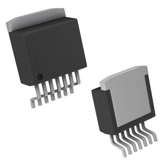
| 产品图片 |
|
| rohs | 符合RoHS无铅 / 符合限制有害物质指令(RoHS)规范要求 |
| 产品系列 | 电源管理 IC,稳压器—开关式稳压器,Exar SP6669AEK-L/TRR3- |
| 数据手册 | http://www.exar.com/Common/Content/Document.ashx?id=1217 |
| 产品型号 | SP6669AEK-L/TRR3 |
| PCN其它 | |
| PWM类型 | 电流模式 |
| 产品种类 | Buck Regulators |
| 供应商器件封装 | SOT-23-5 |
| 其它名称 | 1016-1595-1 |
| 包装 | 剪切带 (CT) |
| 同步整流器 | 是 |
| 商标 | Exar |
| 安装类型 | 表面贴装 |
| 安装风格 | SMD/SMT |
| 封装 | Reel |
| 封装/外壳 | SC-74A,SOT-753 |
| 封装/箱体 | SOT-23-5 |
| 工作温度 | -40°C ~ 85°C |
| 工作温度范围 | - 40 C to + 85 C |
| 工厂包装数量 | 3000 |
| 开关频率 | 1.5 MHz |
| 拓扑结构 | Buck |
| 最大工作温度 | + 85 C |
| 最大输入电压 | 5.5 V |
| 最小工作温度 | - 40 C |
| 最小输入电压 | 2.5 V |
| 标准包装 | 1 |
| 电压-输入 | 2.5 V ~ 5.5 V |
| 电压-输出 | 0.6 V ~ 5 V |
| 电流-输出 | 600mA |
| 类型 | 降压(降压) |
| 负载调节 | 0.5 % |
| 输出数 | 1 |
| 输出电压 | Adj |
| 输出电流 | 600 mA |
| 输出端数量 | 1 |
| 输出类型 | 可调式 |
| 频率-开关 | 1.5MHz |




- 商务部:美国ITC正式对集成电路等产品启动337调查
- 曝三星4nm工艺存在良率问题 高通将骁龙8 Gen1或转产台积电
- 太阳诱电将投资9.5亿元在常州建新厂生产MLCC 预计2023年完工
- 英特尔发布欧洲新工厂建设计划 深化IDM 2.0 战略
- 台积电先进制程称霸业界 有大客户加持明年业绩稳了
- 达到5530亿美元!SIA预计今年全球半导体销售额将创下新高
- 英特尔拟将自动驾驶子公司Mobileye上市 估值或超500亿美元
- 三星加码芯片和SET,合并消费电子和移动部门,撤换高东真等 CEO
- 三星电子宣布重大人事变动 还合并消费电子和移动部门
- 海关总署:前11个月进口集成电路产品价值2.52万亿元 增长14.8%




PDF Datasheet 数据手册内容提取
SP6669 800mA 1.5MHz Synchronous Step Down Converter December 2017 Rev. 3.0.0 GENERAL DESCRIPTION APPLICATIONS The SP6669 is a synchronous current mode • Portable Equipment PWM step down (buck) converter capable of • Battery Operated Equipment delivering up to 800mA of current. It features a pulse skip mode (PSM) for light load efficiency • Audio-Video Equipment and a LDO mode for 100% duty cycle. • Networking & Telecom Equipment With a 2.5V to 6.0V input voltage range and a 1.5MHz switching frequency, the SP6669 allows FEATURES the use of small surface mount inductors and capacitors ideal for battery powered portable • Guaranteed 800mA Output Current applications. The internal synchronous switch − Input Voltage: 2.5V to 6.0V increases efficiency and eliminates the need for an external Schottky diode. Low output • 1.5MHz PWM Current Mode Control voltages are easily supported with the 0.6V − 100% Duty Cycle LDO Mode Operations feedback reference voltage. − Achieves 97% Efficiency Built-in over temperature and output over • 0.6V 2% Accurate Reference voltage lock-out protections insure safe operations under abnormal operating • Excellent Line/Load Transient conditions. Response The SP6669 is offered in a RoHS compliant, • 18µA Quiescent Current “green”/halogen free 5-pin SOT23 package. • Over Temperature Protection • RoHS Compliant “Green”/Halogen Free 5-Pin SOT23 Package TYPICAL APPLICATION DIAGRAM Fig. 1: SP6669 Application Diagram (Adj. version shown) 1/11 Rev.3.0.0
SP6669 800mA 1.5MHz Synchronous Step Down Converter ABSOLUTE MAXIMUM RATINGS OPERATING RATINGS These are stress ratings only and functional operation of Input Voltage Range VIN ............................... 2.5V to 6.0V the device at these ratings or any other above those Operating Temperature Range ................... -40°C to 85°C indicated in the operation sections of the specifications Operating Junction Temperature1 ...........................125°C below is not implied. Exposure to absolute maximum rating conditions for extended periods of time may affect Thermal Resistance θJA .................................. 134.5°C/W reliability. Thermal Resistance θJc ....................................... 81°C/W Input Voltage VIN ....................................... -0.3V to 6.6V Enable VFB Voltage ....................................... -0.3V to VIN Note 1: TJ is a function of the ambient temperature TA and SW Voltage ...................................... -0.3V to (VIN+0.3V) power dissipation PD (TJ= TA + PD x θJA). Peak Switch Sink/Source Current ............................ 1.3A Junction Temperature .......................................... 150°C Storage Temperature .............................. -65°C to 150°C Lead Temperature (Soldering, 10 sec) ................... 260°C ESD Rating (HBM - Human Body Model) .................... 2kV ESD Rating (MM - Machine Model) ........................... 200V ELECTRICAL SPECIFICATIONS Specifications with standard type are for an Operating Junction Temperature of TJ = 25°C only; limits applying over the full Operating Junction Temperature range are denoted by a “•”. Minimum and Maximum limits are guaranteed through test, design, or statistical correlation. Typical values represent the most likely parametric norm at TA = 25°C, and are provided for reference purposes only. Unless otherwise indicated, VIN = 3.6V. Parameter Min. Typ. Max. Units Conditions Feedback Current IVFB ±30 nA Regulated Feedback Voltage VFB 0.588 0.600 0.612 V • Reference Voltage Line Regulation ΔVFB 0.4 %/V • VIN=2.5V to 5.5V Output Over-Voltage Lockout ΔVOVL 20 50 80 mV ΔVOVL = VOVL – VFB (Adj.) Output Voltage Line Regulation ΔVOUT 0.6 %/V • VIN=2.5V to 5.5V Peak Inductor Current IPK 1.2 2.3 A VIN=3V, VFB=0.5V Output Voltage Load Regulation 0.5 % VLOADREG Quiescent Current1 IQ 18 µA VFB=0.65V Shutdown Current ISHTDWN 0.1 1 µA VEN=0V, VIN=4.2V 1.2 1.5 1.8 MHz • VFB=0.6V Oscillator Frequency fOSC 750 kHz • VFB=0V or VOUT=0V RDS(ON) of PMOS RPFET 0.24 Ω ISW=100mA RDS(ON) of NMOS RNFET 0.24 Ω ISW=100mA SW Leakage ILSW ±1 µA VEN=0V, VSW=0V or 5V, VIN=5V Enable Threshold VEN 1.2 V • Shutdown Threshold VEN 0.4 V • EN Leakage Current IEN ±1 µA • Note 1: The dynamic quiescent current is higher due to the gate charge being delivered at the switching frequency. 2/11 Rev. 3.0.0
SP6669 800mA 1.5MHz Synchronous Step Down Converter BLOCK DIAGRAM Fig. 2: SP6669 Block Diagram PIN ASSIGNMENT Fig. 3: SP6669 Pin Assignment 3/11 Rev. 3.0.0
SP6669 800mA 1.5MHz Synchronous Step Down Converter PIN DESCRIPTION Name Pin Number Description Enable Pin. Do not leave the pin floating. EN 1 VEN<0.4V: Shutdown mode VEN>1.2V: Device enabled GND 2 Ground Signal SW 3 Switching Node Power Supply Pin. VIN 4 Must be decoupled to ground with a 4.7µF or greater ceramic capacitor. Feedback Input Pin. VFB 5 Connect VFB to the center point of the resistor divider. ORDERING INFORMATION(1) Part Number Operating Temperature Range Lead-free Package Packing Method SP6669AEK-L/TRR3 -40°C≤TA≤+85°C Yes(2) SOT23-5 Tape & Reel SP6669EB SP6669 Evaluation Board Note: 1. Refer to www.exar.com/SP6669 for most up-to-date Ordering Information 2. Visit www.exar.com for additional information on Environmental Rating Note that the SP6669 series is packaged in Tape and Reel with a reverse part orientation as per the following diagram 4/11 Rev. 3.0.0
SP6669 800mA 1.5MHz Synchronous Step Down Converter TYPICAL PERFORMANCE CHARACTERISTICS All data taken at VIN = 2.7V to 5.5V, TJ = TA = 25°C, unless otherwise specified - Schematic and BOM from Application Information section of this datasheet. Fig. 4: Efficiency vs Output Current VOUT = 1.2V Fig. 5: Oscillator Frequency vs. Input Voltage Fig. 6: EN Pin Threshold vs. Input Voltage Fig. 7: EN Pin Threshold vs. Temperature Fig. 8: UVLO Threshold vs. Temperature Fig. 9: Output Voltage vs Temperature 5/11 Rev. 3.0.0
SP6669 800mA 1.5MHz Synchronous Step Down Converter Fig. 10: Line Regulation Fig. 11: Load Regulation Fig. 12: Load Transient Response, Iout 250mA to 500mA, Fig. 13: Load Transient Response, Iout 10mA to 500mA, Vout = 1.2V Vout = 1.2V Fig. 14: PSM / PWM Boundaries Fig. 15: Output Voltage Ripple vs Output Current 6/11 Rev. 3.0.0
SP6669 800mA 1.5MHz Synchronous Step Down Converter Fig. 16: Power-ON from EN Pin Fig. 17: Power-OFF from EN Pin Fig. 18: PWM Operation Fig. 19: Short Circuit Response 7/11 Rev. 3.0.0
SP6669 800mA 1.5MHz Synchronous Step Down Converter THEORY OF OPERATION stability, its value can be optimized to balance very low output ripple and circuit size. It is APPLICATIONS recommended to use an X5R or X7R rated capacitors which have the best temperature and voltage characteristics of all the ceramics for a given value and size. SETTING OUTPUT VOLTAGE The output voltage is determined by: R Eq. 4: V =0.6V ⋅1+ 2 Fig. 20: Typical Application Circuit OUT R 1 THERMAL CONSIDERATIONS INDUCTOR SELECTION Although the SP6669 has an on board over Inductor ripple current and core saturation are temperature circuitry, the total power two factors considered to select the inductor dissipation it can support is based on the value. package thermal capabilities. The formula to 1 V ensure safe operation is given in note 1. Eq. 1: ∆I = V 1− OUT L f ⋅L OUT V IN PCB LAYOUT Equation 1 shows the inductor ripple current as The following PCB layout guidelines should be a function of the frequency, inductance, VIN and taken into account to ensure proper operation VOUT. It is recommended to set the ripple and performance of the SP6669: current between 30% to 40% of the maximum load current. A low ESR inductor is preferred. 1- The GND, SW and VIN traces should be kept short, direct and wide. CIN AND COUT SELECTION 2- VFB pin must be connected directly to the feedback resistors. The resistor divider network A low ESR input capacitor can prevent large voltage transients at VIN. The RMS current must be connected in parallel to the COUT capacitor. rating of the input capacitor is required to be larger than IRMS calculated by: 3- The input capacitor CIN must be kept as close V (V −V ) as possible to the VIN pin. Eq. 2: I ≅ I OUT IN OUT 4- The SW and VFB nodes should be kept as RMS OMAX V IN separate as possible to minimize possible effects from the high frequency and voltage The ESR rating of the capacitor is an important swings of the SW node. parameter to select COUT. The output ripple VOUT is determined by: 5- The ground plates of CIN and COUT should be kept as close as possible. 1 Eq. 3: ∆V ≅∆I ESR+ OUT L 8⋅ f ⋅C OUT Higher values, lower cost ceramic capacitors are now available in smaller sizes. These capacitors have high ripple currents, high voltage ratings and low ESR that makes them ideal for switching regulator applications. As COUT does not affect the internal control loop 8/11 Rev. 3.0.0
SP6669 800mA 1.5MHz Synchronous Step Down Converter OUTPUT VOLTAGE RIPPLE FOR VIN CLOSE TO DESIGN EXAMPLE V OUT In a single Lithium-Ion battery powered When the input voltage VIN is close to the output application, the VIN range is about 2.7V to 4.2V. voltage VOUT, the SP6669 transitions smoothly The desired output voltage is 1.8V. from the switching PWM converter mode into a The inductor value needed can be calculated LDO mode. The following diagram shows the using the following equation output voltage ripple versus the input voltage for a 3.3V output setting and a 200mA current 1 V L= V 1− OUT load. f ⋅∆I OUT V L IN Substituting VOUT=1.8V, VIN=4.2V, ΔIL=180mA to 240mA (30% to 40%) and f=1.3MHz gives A 3.3µH inductor can be chosen with this 𝐿𝐿 = 2.86𝜇𝜇𝜇𝜇 𝑡𝑡𝑡𝑡 3.81𝜇𝜇𝜇𝜇 application. An inductor of greater value with less equivalent series resistance would provide better efficiency. The CIN capacitor requires an RMS current rating of at least ILOAD(MAX)/2 and low ESR. In most cases, a ceramic capacitor will Fig. 20: VOUT Ripple Voltage satisfy this requirement. for VIN decreasing close to VOUT 9/11 Rev. 3.0.0
SP6669 800mA 1.5MHz Synchronous Step Down Converter MECHANICAL DIMENSIONS 5-PIN SOT23 10/11 Rev. 3.0.0
SP6669 800mA 1.5MHz Synchronous Step Down Converter REVISION HISTORY Revision Date Description Reformat of datasheet 2.0.0 07/15/2011 Updated package specification 2.1.0 02/07/2012 Updated Typical Application schematics and Design example Reformat of datasheet (New logo) 2.2.0 11/08/2012 Updated Absolute Maximum Ratings, Lead Temperature (Soldering, 10 sec) to 260°C Reformat of datasheet (New logo) 2.2.1 05/13/2016 Changed oscillator frequency unit Updated IOUT, VIN range, thermal resistance, ∆VOUT, VFB temperature condition, IPK, IQ, 3.0.0 12/07/2017 fOSC, RDS(ON), package drawing (now Mechanical Dimensions), format and Ordering Information. Added PSM and new graphs. Updated to MaxLinear logo. Removed fixed voltage options. New graphs. Corporate Headquarters: High Performance Analog 5966 La Place Court 1060 Rincon Circle Suite 100 San Jose, CA 95131 Carlsbad, CA 92008 Tel.: +1 (669) 265 6100 Tel.:+1 (760) 692-0711 Fax: +1 (669) 265 6101 Fax: +1 (760) 444-8598 Email: powertechsupport@exar.com www.maxlinear.com www.exar.com The content of this document is furnished for informational use only, is subject to change without notice, and should not be construed as a commitment by MaxLinear, Inc.. MaxLinear, Inc. assumes no responsibility or liability for any errors or inaccuracies that may appear in the informational content contained in this guide. Complying with all applicable copyright laws is the responsibility of the user. Without limiting the rights under copyright, no part of this document may be reproduced into, stored in, or introduced into a retrieval system, or transmitted in any form or by any means (electronic, mechanical, photocopying, recording, or otherwise), or for any purpose, without the express written permission of MaxLinear, Inc. Maxlinear, Inc. does not recommend the use of any of its products in life support applications where the failure or malfunction of the product can reasonably be expected to cause failure of the life support system or to significantly affect its safety or effectiveness. Products are not authorized for use in such applications unless MaxLinear, Inc. receives, in writing, assurances to its satisfaction that: (a) the risk of injury or damage has been minimized; (b) the user assumes all such risks; (c) potential liability of MaxLinear, Inc. is adequately protected under the circumstances. MaxLinear, Inc. may have patents, patent applications, trademarks, copyrights, or other intellectual property rights covering subject matter in this document. Except as expressly provided in any written license agreement from MaxLinear, Inc., the furnishing of this document does not give you any license to these patents, trademarks, copyrights, or other intellectual property. Company and product names may be registered trademarks or trademarks of the respective owners with which they are associated. © 2016 – 2017 MaxLinear, Inc. All rights reserved. 11/11 Rev. 3.0.0
Mouser Electronics Authorized Distributor Click to View Pricing, Inventory, Delivery & Lifecycle Information: E xar: SP6669AEK-L/TRR3

 Datasheet下载


