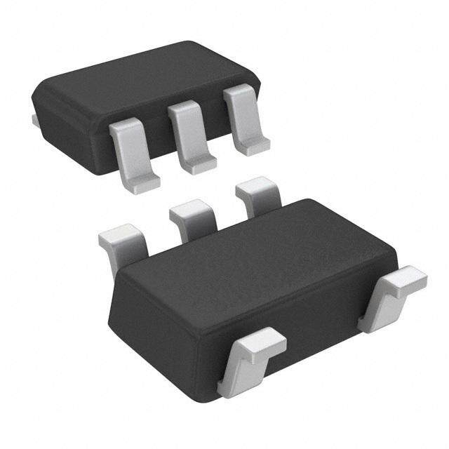
ICGOO在线商城 > 集成电路(IC) > PMIC - 稳压器 - 线性 > SP6203EM5-L-3-3
- 型号: SP6203EM5-L-3-3
- 制造商: Exar
- 库位|库存: xxxx|xxxx
- 要求:
| 数量阶梯 | 香港交货 | 国内含税 |
| +xxxx | $xxxx | ¥xxxx |
查看当月历史价格
查看今年历史价格
SP6203EM5-L-3-3产品简介:
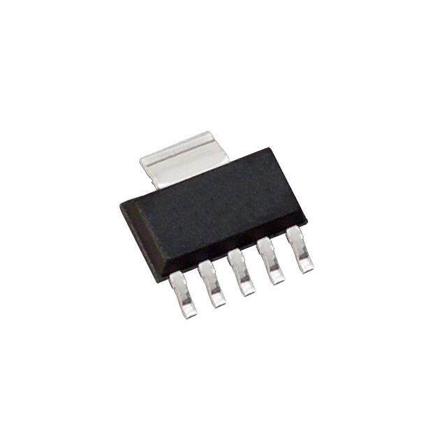
ICGOO电子元器件商城为您提供SP6203EM5-L-3-3由Exar设计生产,在icgoo商城现货销售,并且可以通过原厂、代理商等渠道进行代购。 SP6203EM5-L-3-3价格参考。ExarSP6203EM5-L-3-3封装/规格:PMIC - 稳压器 - 线性, Linear Voltage Regulator IC Positive Fixed 1 Output 3.3V 300mA SOT-23-5。您可以下载SP6203EM5-L-3-3参考资料、Datasheet数据手册功能说明书,资料中有SP6203EM5-L-3-3 详细功能的应用电路图电压和使用方法及教程。
| 参数 | 数值 |
| 产品目录 | 集成电路 (IC)半导体 |
| 描述 | IC REG LDO 3.3V 0.3A SOT23-5低压差稳压器 Micropower, 300mA CMOS LDO Regulators |
| 产品分类 | |
| 品牌 | Exar Corporation |
| 产品手册 | |
| 产品图片 |
|
| rohs | 符合RoHS无铅 / 符合限制有害物质指令(RoHS)规范要求 |
| 产品系列 | 电源管理 IC,低压差稳压器,Exar SP6203EM5-L-3-3- |
| 数据手册 | http://www.exar.com/Common/Content/Document.ashx?id=653 |
| 产品型号 | SP6203EM5-L-3-3 |
| PCN设计/规格 | |
| PSRR/纹波抑制—典型值 | 67 dB |
| 产品种类 | 低压差稳压器 |
| 供应商器件封装 | SOT-23-5 |
| 其它名称 | 1016-1205 |
| 包装 | 散装 |
| 商标 | Exar |
| 回动电压—最大值 | 300 mV |
| 安装类型 | 表面贴装 |
| 安装风格 | SMD/SMT |
| 封装/外壳 | SC-74A,SOT-753 |
| 封装/箱体 | SOT-23-5 |
| 工作温度 | -40°C ~ 125°C |
| 最大工作温度 | + 125 C |
| 最大输入电压 | 6 V |
| 最小工作温度 | - 40 C |
| 最小输入电压 | 2.7 V |
| 标准包装 | 250 |
| 电压-跌落(典型值) | 0.18V @ 300mA |
| 电压-输入 | 最高 5.5V |
| 电压-输出 | 3.3V |
| 电压调节准确度 | 2 % |
| 电流-输出 | 300mA |
| 电流-限制(最小值) | 330mA |
| 稳压器拓扑 | 正,固定式 |
| 稳压器数 | 1 |
| 线路调整率 | 0.04 %/V |
| 负载调节 | 0.07 % |
| 输出电压 | 3.3 V |
| 输出电流 | 300 mA |
| 输出端数量 | 1 Output |
| 输出类型 | Fixed |




- 商务部:美国ITC正式对集成电路等产品启动337调查
- 曝三星4nm工艺存在良率问题 高通将骁龙8 Gen1或转产台积电
- 太阳诱电将投资9.5亿元在常州建新厂生产MLCC 预计2023年完工
- 英特尔发布欧洲新工厂建设计划 深化IDM 2.0 战略
- 台积电先进制程称霸业界 有大客户加持明年业绩稳了
- 达到5530亿美元!SIA预计今年全球半导体销售额将创下新高
- 英特尔拟将自动驾驶子公司Mobileye上市 估值或超500亿美元
- 三星加码芯片和SET,合并消费电子和移动部门,撤换高东真等 CEO
- 三星电子宣布重大人事变动 还合并消费电子和移动部门
- 海关总署:前11个月进口集成电路产品价值2.52万亿元 增长14.8%




PDF Datasheet 数据手册内容提取
SSPP66220033 // SSPP66220055 330000mmAA//550000mmAA LLooww NNooiissee CCMMOOSS LLDDOO RReegguullaattoorrss August 2018 Rev. 2.0.1 GENERAL DESCRIPTION APPLICATIONS The SP6203 and SP6205 are ultra low noise • Battery-Powered Systems CMOS LDOs with very low dropout and ground • Medical Equipments current. The noise performance is achieved by means of an external bypass capacitor without • MP3/CD Players sacrificing turn-on and turn-off speed critical • Digital Cameras to portable applications. Extremely stable and easy to use, these devices offer excellent PSRR and Line/Load regulation. Target FEATURES applications include battery-powered • 300mA/500mA Output Current equipment such as portable and wireless products. Regulators' ground current increases − SP6203: 300mA – SP6205: 500mA only slightly in dropout. Fast turn-on/turn-off − Low Dropout Voltage: 0.6Ω PMOS FET enable control and an internal 30Ω pull down • 2.7V to 5.5V Input Voltage on output allows quick discharge of output even under no load conditions. Both LDOs are − Fixed and Adjustable Output Voltage protected with current limit and thermal − Accurate Output Voltage: 2% over Temp. shutdown. • 67dB Power Supply Rejection Ratio The SP6205 is available in fixed & adjustable output voltage versions and come in an • 12μVRMS Low Output Noise industry standard 5-pin SOT-23 and small • Unconditionally Stable with 2.2μF 2X3mm 8-pin DFN packages. For SC-70 Ceramic 100mA CMOS LDO, SP6213 is available. • Low Quiescent Current: 5μA • Low Ground Current: 350μA at 500mA • Fast Turn-On and Turn-Off: 60μS • Very Good Load/Line Regulation: 0.07/0.04 % • Current Limit and Thermal Protection • RoHS Compliant “Green”/Halogen Free 5-Pin SOT23 and 8-Pin DFN Packages TYPICAL APPLICATION DIAGRAM Fig. 1: SP6203/SP6205 Application Diagram 1/15 Rev. 2.0.1
SSPP66220033 // SSPP66220055 330000mmAA//550000mmAA LLooww NNooiissee CCMMOOSS LLDDOO RReegguullaattoorrss ABSOLUTE MAXIMUM RATINGS OPERATING RATINGS These are stress ratings only and functional operation of Input Voltage Range VIN .......................... +2.7V to +5.5V the device at these ratings or any other above those Enable Input Voltage VEN................ ... ...............0 to 5.5V indicated in the operation sections of the specifications Junction Temperature Range ................. -40°C to +125°C below is not implied. Exposure to absolute maximum Thermal Resistance ...................................................... rating conditions for extended periods of time may affect reliability. SOT-23-5 (θJA) .............................................191°C/W DFN-8 (θJA) ................................................... 59°C/W VIN .............................................................. -2V to 6.0V Output Voltage VOUT .............................. -0.6V to VIN +1V Note 1: Maximum power dissipation can be calculated Enable Input Voltage VEN................ .. ...............-2V to 6V using the formula: PD = (TJ (max) - TA) / θJA, where Storage Temperature .............................. -65°C to 150°C TJ(max) is the junction temperature, TA is the ambient Power Dissipation ............................... Internally Limited1 temperature and θJA is the junction-to-ambient thermal Lead Temperature (Soldering, 5 sec) ................... +260°C resistance. θJC is 6°C/W for this package. Exceeding the maximum allowable power dissipation will result in Junction Temperature ........................................ +150°C excessive die temperature and the regulator will go into thermal shutdown mode. ELECTRICAL SPECIFICATIONS Specifications with standard type are for an Operating Junction Temperature of TJ = 25°C only; limits applying over the full Operating Junction Temperature range are denoted by a “•”. Minimum and Maximum limits are guaranteed through test, design, or statistical correlation. Typical values represent the most likely parametric norm at TJ = 25°C, and are provided for reference purposes only. Unless otherwise indicated, VIN = (VOUT + 0.5V) to 6V, CIN = 2.2µF, COUT = 2.2µF and IOUT = 100µA, TJ= –40°C to 85°C. Parameter Min. Typ. Max. Units Conditions Input Voltage 6 V • Output Voltage -2 +2 % • Variation from specified VOUT Output Voltage Temperature Coefficient2 50 ppm/°C ∆ VOUT/∆T Reference Voltage 1.225 1.25 1.275 V • Adjustable version only Line Regulation 0.04 0.3 %/V ∆VOUT (VIN below 6V) Load Regulation3 0.07 0.3 % IOUT = 0.1mA to 300mA (SP6203) 0.13 0.5 IOUT = 0.1mA to 500mA (SP6205) 0.06 IOUT = 0.1mA 60 IOUT = 100mA Dropout Voltage for VOUT ≥ 3.0V4 120 mV IOUT = 200mA 180 300 • IOUT = 300mA (SP6203) 300 500 • IOUT = 500mA (SP6205) 45 100 • IOUT = 0.1mA (IQUIESCENT) 110 IOUT = 100mA Ground Pin Current5 175 µA IOUT = 200mA 235 330 • IOUT = 300mA (SP6203) 350 490 • IOUT = 500mA (SP6205) Shutdown Supply Current 0.01 1 µA • VEN < 0.4V (shutdown) Current Limit 0.33 0.50 0.8 A VOUT = 0V (SP6203) 0.55 0.85 1.4 VOUT = 0V (SP6205) Thermal Shutdown Junction 170 °C Regulator Turns off Temperature Thermal Shutdown Hysteresis 12 °C Regulator turns on again at 158°C Power Supply Rejection Ratio 67 dB f ≤ 1kHz 150 CBYP = 0nF, IOUT = 0.1mA Output Noise Voltage6 61320 µVRMS CCBBYYPP == 010nFn,F ,I OIUOTU T= = 3 000.1mmAA 50 75 CBYP = 10nF, IOUT = 300mA Thermal Regulation7 0.05 %/W ∆VOUT / ∆PD Wake-Up Time (TWU)8 25 50 µS VIN ≥ 4V10 (from shutdown mode) IOUT = 30mA 2/15 Rev. 2.0.1
SSPP66220033 // SSPP66220055 330000mmAA//550000mmAA LLooww NNooiissee CCMMOOSS LLDDOO RReegguullaattoorrss Parameter Min. Typ. Max. Units Conditions Turn-On Time (TON)9 60 120 µS VIN ≥ 4V10 (from shutdown mode) IOUT = 30mA Turn-Off Time (TOFF) 11050 22550 µS IIOOUUTT == 030.10mmAA,, VVIINN ≥≥ 44VV1100 Output Discharge Resistance 30 Ω No Load Enable Input Logic Low Voltage 0.4 V • Regulator Shutdown Enable Input Logic High Voltage 1.6 V • Regulator Enabled Note 2: Output voltage temperature coefficient is defined as the worst case voltage change divided by the total temperature range. Note 3: Regulation is measured at constant junction temperature using low duty cycle pulse testing. Changes in output voltage due to heating effects are covered by the thermal regulation specification. Note 4: Dropout-voltage is defined as the input to output differential at which the output voltage drops 2% below its nominal value measured at 1V differential. Note 5: Ground pin current is the regulator quiescent current. The total current drawn from the supply is the sum of the load current plus the ground pin current. Note 6: Output noise voltage is defined within a certain bandwidth, namely 10Hz < BW < 100kHz. An external bypass cap (10nF) from reference output (BYP pin) to ground significantly reduces noise at output. Note 7: Thermal regulation is defined as the change in output voltage at a time “t” after a change in power dissipation is applied, excluding load and line regulation effects. Specifications are for a 300mA load pulse at VIN = 6V for t = 1ms. Note 8: The wake-up time (TWU) is defined as the time it takes for the output to start rising after enable is brought high. Note 9: The total turn-on time is called the settling time (TS), which is defined as the condition when both the output and the bypass node are within 2% of their fully enabled values when released from shutdown. Note 10: For output voltage versions requiring VIN to be lower than 4V, timing (TON & TOFF) increases slightly. BLOCK DIAGRAM Fig. 2: SP6203/SP6205 Functional Diagram 3/15 Rev. 2.0.1
SSPP66220033 // SSPP66220055 330000mmAA//550000mmAA LLooww NNooiissee CCMMOOSS LLDDOO RReegguullaattoorrss PIN ASSIGNMENT 5-Pin SOT23 8-Pin DFN Fig. 3: SP6203/SP6205 Pin Assignment PIN DESCRIPTION Name SOT-23-5 Description VIN 1 Power Supply Input GND 2 Ground Terminal Enable/Shutdown EN 3 - Logic high = enable - Logic low = shutdown Bypass - Fixed voltage option: Reference bypass input for ultra-quiet operation. Connecting a 10nF cap on this pin reduces output noise. BYP/ADJ 4 Adjustable Input – Adjustable voltage option: Adjustable regulator feedback input. Connect to a resistive voltage- Divider network. VOUT 5 Regulator Output Voltage Name DFN-8 Description Adjustable Input – Adjustable voltage option: ADJ 1 Adjustable regulator feedback input. Connect to a resistive voltage- Divider network. NC 2 No Connect GND 3 Ground Terminal Enable/Shutdown EN 4 - Logic high = enable - Logic low = shutdown VIN 5 Power Supply Input NC 6 No Connect NC 7 No Connect VOUT 8 Regulator Output Voltage 4/15 Rev. 2.0.1
SSPP66220033 // SSPP66220055 330000mmAA//550000mmAA LLooww NNooiissee CCMMOOSS LLDDOO RReegguullaattoorrss ORDERING INFORMATION(1) Ambient Temperature Part Number Lead-Free Package Packing Method Voltage Option Range SP6203EM5-L-2-8/TR 2.8V SP6205EM5-L/TR ADJ SOT-23-5 SP6205EM5-L-3-0/TR -40°C≤TA≤+125°C Yes(2) Tape & Reel 3.0V SP6205EM5-L-3-3/TR 3.3V SP6205ER-L/TR DFN8 ADJ NOTES: 1. Refer to www.exar.com/SP6203 and www.exar.com/SP6205 for most up-to-date Ordering Information. 2. Visit www.exar.com for additional information on Environmental Rating. 5/15 Rev. 2.0.1
SSPP66220033 // SSPP66220055 330000mmAA//550000mmAA LLooww NNooiissee CCMMOOSS LLDDOO RReegguullaattoorrss TYPICAL PERFORMANCE CHARACTERISTICS All data taken at VIN = 2.7V to 5.5V, TJ = TA = 25°C, unless otherwise specified - Schematic and BOM from Application Information section of this datasheet. Fig. 4: Current Limit Fig. 5: Turn-On Time, RLOAD=50Ω (60mA) Fig. 6: Turn-Off Time, RLOAD=6Ω (500mA) Fig. 7: Turn-Off Time, RLOAD=30KΩ (0.1mA) Fig. 8: Load Regulation, IO=100µA ~500mA Fig. 9: Regulation, Line Step from 4V to 6V, IO=1mA 6/15 Rev. 2.0.1
SSPP66220033 // SSPP66220055 330000mmAA//550000mmAA LLooww NNooiissee CCMMOOSS LLDDOO RReegguullaattoorrss Fig. 10: Start Up Waveform, VIN=3.5V, IO=500mA Fig. 11: Start Up Waveform, Slow VIN , No Load Fig. 12: Start Up Waveform, Slow VIN, 500mA Output Load Fig. 13: Start Up Waveform, Slow VIN, COUT=1000μF, IO=0mA Fig. 14: Start Up Waveform, Slow VIN, Fig. 15: Fast VIN, No Load COUT=1000μF, IO=500mA 7/15 Rev. 2.0.1
SSPP66220033 // SSPP66220055 330000mmAA//550000mmAA LLooww NNooiissee CCMMOOSS LLDDOO RReegguullaattoorrss Fig. 16: Fast VIN, 500mA Output Load Fig. 17: Fast VIN = 1000μF Output Load Fig. 18: Fast VIN , COUT=1000μF, IO=500mA Fig. 19: Output Noise, CBYP = 10nF Fig. 20: Output Noise, CBYP = open 8/15 Rev. 2.0.1
SSPP66220033 // SSPP66220055 330000mmAA//550000mmAA LLooww NNooiissee CCMMOOSS LLDDOO RReegguullaattoorrss THEORY OF OPERATION or tantalum capacitor may be used at the input. GENERAL OVERVIEW OUTPUT CAPACITOR The SP6203/6205 is intended for applications where very low dropout voltage, low supply An output capacitor is required between VOUT current and low output noise are critical, even and GND to prevent oscillation. A 2.2μF output with high load conditions (500mA maximum). capacitor is recommended. Unlike bipolar regulators, the SP6203/6205 Larger values make the chip more stable (CMOS LDO) supply current increases only which means an improvement of the slightly with load current. regulator’s transient response. Also, when The SP6203/6205 contains an internal operating from other sources than batteries, bandgap reference which is fed into the supply-noise rejection can be improved by inverting input of the LDO-amplifier. The increasing the value of the input and output output voltage is then set by means of a capacitors and using passive filtering resistor divider and compared to the bandgap techniques. reference voltage. The error LDO-amplifier For a lower output current, a smaller output drives the gate of a P-channel MOSFET pass capacitance can be chosen. device that has a RDS(ON) of 0.6Ω at 500mA producing a 300mV drop at the output. Finally, the output capacitor should have an effective series resistance (ESR) of 0.5Ω or Furthermore, the SP6203/6205 has its own less. current limit circuitry (500mA/850mA) to ensure that the output current will not damage Therefore, the use of good quality ceramic or the device during output short, overload or tantalum capacitors is advised. start-up. BYPASS CAPACITOR Also, the SP6203/6205 includes thermal shut-down circuitry to turn off the device when A bypass pin (BYP) is provided to decouple the the junction temperature exceeds 170°C and it bandgap reference. A 10nF external capacitor re-mains off until the temperature drops by connected from BYP to GND reduces noise 12°C. present on the internal reference, which in turn significantly reduces output noise and ENABLE/SHUTDOWN OPERATION also improves power supply rejection. Note that the minimum value of COUT must be The SP6203/6205 is turned off by pulling the increased to maintain stability when the VEN pin below 0.4V and turned on by pulling it bypass capacitor is used because CBYP reduces above 1.6V. the regulator phase margin. If output noise is If this enable/shutdown feature is not not a concern, this input may be left required, it should be tied directly to the input unconnected. Larger capacitor values may be supply voltage to keep the regulator output on used to further improve power supply at all time. rejection, but result in a longer time period (slower turn on) to settle output voltage when While in shutdown, VOUT quickly falls to zero power is initially applied. (turn-off time is dependent on load conditions and output capacitance on VOUT) and power NO LOAD STABILITY consumption drops nearly to zero. The SP6203/6205 will remain stable and in INPUT CAPACITOR regulation with no external load (other than the internal voltage driver) unlike many other A small capacitor of 2.2μF is required from VIN voltage regulators. This is especially important to GND if a battery is used as the power in CMOS RAM battery back-up applications. source. Any good quality electrolytic, ceramic 9/15 Rev. 2.0.1
SSPP66220033 // SSPP66220055 330000mmAA//550000mmAA LLooww NNooiissee CCMMOOSS LLDDOO RReegguullaattoorrss TURN ON TIME TJ(max) is the maximum junction temperature of the die and is 125°C. TA is the ambient The turn on response is split up in two temperature. θJA is the junction-to-ambient separate response categories: the wake up thermal resistance for the regulator and is time (TWU) and the settling time (TS). The layout dependent. The SOT-23-5 package has wake up time is defined as the time it takes a θJA of approximately 191°C/W for minimum for the output to rise to 2% of its total value PCB copper footprint area. after being released from shutdown (EN > 0.4V). The settling time is defined as the This results in a maximum power dissipation condition where the output reaches 98% of its of: total value after being released from PD(max)=[(125°C-25°C)/(191°C/W)] = 523mW shutdown. The latter is also called the turn on time and is dependent on the output capacitor, The actual power dissipation of the regulator a little bit on load and, if present, on a bypass circuit can be determined using one simple capacitor. equation: PD = (VIN - VOUT) * IOUT + VIN * IGND To prevent the device from entering thermal shutdown, maximum power dissipation cannot be exceeded. Substituting PD(max) for PD and solving for the operating conditions that are critical to the application will give the maximum operating conditions for the regulator circuit. For example, if we are operating the SP6203 3.0V TURN OFF TIME at room temperature, with a minimum footprint layout and output current of 300mA, The turn off time is defined as the condition the maximum input voltage can be where the output voltage drops about 66% (θ) determined, based on the equation below. of its total value. 5θ to 7θ is the constant Ground pin current can be taken from the where the output voltage drops nearly to zero. electrical specifications table (0.23mA at There will always be a small voltage drop in 300mA). shutdown because of the switch unless we short-circuit it. The turn off time of the output 390mW = (VIN-3.0V) * 300mA + VIN * 0.23mA voltage is dependent on load conditions, After calculations, we find that the maximum output capacitance on VOUT (time constant τ = input voltage of a 3.0V application at 300mA RLCL) and also on the difference in voltage of output current in a SOT-23-5 package is between input and output. 4.7V. So if the intent is to operate a 5V output THERMAL CONSIDERATIONS version from a 6V supply at 300mA load and The SP6203/6205 is designed to provide at a 25°C ambient temperature, then the 300/500mA of continuous current in a tiny actual total power dissipation will be: package. Maximum power dissipation can be P =([6V-5V]*[300mA])+(6V*0.23mA)=301.4mW D calculated based on the output current and the voltage drop across the part. To determine the This is well below the 523mW package maxi- maximum power dissipation of the package, mum. Therefore, the regulator can be used. use the junction-to-ambient thermal Note that the regulator cannot always be used resistance of the device and the following at its maximum current rating. For example, in basic equation: a 5V input to 3.0V output application at an PD = (TJ(max) - TA) / θJA ambient temperature of 25°C and operating at the full 500mA (IGND=0.355mA) load, the 10/15 Rev. 2.0.1
SSPP66220033 // SSPP66220055 330000mmAA//550000mmAA LLooww NNooiissee CCMMOOSS LLDDOO RReegguullaattoorrss regulator is limited to a much lower load LAYOUT CONSIDERATIONS current, determined by the following equation: The primary path of heat conduction out of the 523mW = ( [5V-3V]*[ Iload(max)]) +(5V*0.350mA) package is via the package leads. Therefore, careful considerations have to be taken into account: After calculation, we find that in such an application (SP6205) the regulator is limited to 1) Attaching the part to a larger copper 260.6mA. Doing the same calculations for the footprint will enable better heat transfer from 300mA LDO (SP6203) will limit the regulator’s the device, especially on PCB’s where there output current to 260.9mA. are internal ground and power planes. Also, taking advantage of the very low dropout 2) Place the input, output and bypass voltage characteristics of the SP6203/6205, capacitors close to the device for optimal power dissipation can be reduced by using the transient response and device behavior. lowest possible input voltage to minimize the 3) Connect all ground connections directly to input-to-output drop. the ground plane. In case there’s no ground plane, connect to a common local ground point ADJUSTABLE REGULATOR APPLICATIONS before connecting to board ground. The SP6203/6205 can be adjusted to a specific Such layouts will provide a much better output voltage by using two external resistors thermal conductivity (lower θJA) for, a higher (see functional diagram). The resistors set the maximum allowable power dissipation limit. output voltage based on the following equation: VOUT = VREF * (R1/R2 + 1) Resistor values are not critical because ADJ (adjust) has a high input impedance, but for best performance use resistors of 470KΩ or less. DUAL-SUPPLY OPERATION When used in dual supply systems where the regulator load is returned to a negative supply, the output voltage must be diode clamped to ground. 11/15 Rev. 2.0.1
SSPP66220033 // SSPP66220055 330000mmAA//550000mmAA LLooww NNooiissee CCMMOOSS LLDDOO RReegguullaattoorrss MECHANICAL DIMENSIONS 8-PIN DFN 2X3 12/15 Rev. 2.0.1
SSPP66220033 // SSPP66220055 330000mmAA//550000mmAA LLooww NNooiissee CCMMOOSS LLDDOO RReegguullaattoorrss RECOMMENDED LAND PATTERN AND STENCIL 8-PIN DFN 2X3 13/15 Rev. 2.0.1
SSPP66220033 // SSPP66220055 330000mmAA//550000mmAA LLooww NNooiissee CCMMOOSS LLDDOO RReegguullaattoorrss MECHANICAL DIMENSIONS 5-PIN SOT-23 14/15 Rev. 2.0.1
SSPP66220033 // SSPP66220055 330000mmAA//550000mmAA LLooww NNooiissee CCMMOOSS LLDDOO RReegguullaattoorrss REVISION HISTORY Revision Date Description Reformatted Data Sheet 2.0.0 04/03/2012 Includes top package marking update. Updated to MaxLinear logo. Updated format and Ordering Information. Updated 2.0.1 08/31/2018 Adjustable Regulator Applications section. Removed obsolete Fixed Voltage DFN option. Corrected output noise voltage conditions in Electrical Specifications. Corporate Headquarters: 5966 La Place Court Suite 100 Carlsbad, CA 92008 Tel.:+1 (760) 692-0711 Fax: +1 (760) 444-8598 www.maxlinear.com High Performance Analog: 1060 Rincon Circle San Jose, CA 95131 Tel.: +1 (669) 265-6100 Fax: +1 (669) 265-6101 www.exar.com The content of this document is furnished for informational use only, is subject to change without notice, and should not be construed as a commitment by MaxLinear, Inc.. MaxLinear, Inc. assumes no responsibility or liability for any errors or inaccuracies that may appear in the informational content contained in this guide. Complying with all applicable copyright laws is the responsibility of the user. Without limiting the rights under copyright, no part of this document may be reproduced into, stored in, or introduced into a retrieval system, or transmitted in any form or by any means (electronic, mechanical, photocopying, recording, or otherwise), or for any purpose, without the express written permission of MaxLinear, Inc. Maxlinear, Inc. does not recommend the use of any of its products in life support applications where the failure or malfunction of the product can reasonably be expected to cause failure of the life support system or to significantly affect its safety or effectiveness. Products are not authorized for use in such applications unless MaxLinear, Inc. receives, in writing, assurances to its satisfaction that: (a) the risk of injury or damage has been minimized; (b) the user assumes all such risks; (c) potential liability of MaxLinear, Inc. is adequately protected under the circumstances. MaxLinear, Inc. may have patents, patent applications, trademarks, copyrights, or other intellectual property rights covering subject matter in this document. Except as expressly provided in any written license agreement from MaxLinear, Inc., the furnishing of this document does not give you any license to these patents, trademarks, copyrights, or other intellectual property. Company and product names may be registered trademarks or trademarks of the respective owners with which they are associated. © 2012 - 2018 MAXLINEAR, INC. ALL RIGHTS RESERVED 15/15 Rev. 2.0.1

 Datasheet下载


