 Datasheet下载
- 型号: SP4020-01FTG
- 制造商: Littelfuse
- 库位|库存: xxxx|xxxx
- 要求:
| 数量阶梯 | 香港交货 | 国内含税 |
| +xxxx | $xxxx | ¥xxxx |
查看当月历史价格
查看今年历史价格
SP4020-01FTG产品简介:
ICGOO电子元器件商城为您提供SP4020-01FTG由Littelfuse设计生产,在icgoo商城现货销售,并且可以通过原厂、代理商等渠道进行代购。 SP4020-01FTG价格参考¥2.09-¥2.09。LittelfuseSP4020-01FTG封装/规格:TVS - 二极管, 。您可以下载SP4020-01FTG参考资料、Datasheet数据手册功能说明书,资料中有SP4020-01FTG 详细功能的应用电路图电压和使用方法及教程。
| 参数 | 数值 |
| 产品目录 | |
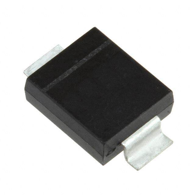
| 描述 | TVS DIODE 3.3VWM 21.8VC SOD323TVS二极管阵列 2.5pF 30A for Surge Protection |
| 产品分类 | |
| 品牌 | Littelfuse Inc |
| 产品手册 | |
| 产品图片 |
|
| rohs | 符合RoHS无铅 / 符合限制有害物质指令(RoHS)规范要求 |
| 产品系列 | 二极管与整流器,TVS二极管,TVS二极管阵列,Littelfuse SP4020-01FTGSP4020, SPA® |
| 数据手册 | |
| 产品型号 | SP4020-01FTG |
| 不同频率时的电容 | 2.5pF @ 1MHz |
| 产品培训模块 | http://www.digikey.cn/PTM/IndividualPTM.page?site=cn&lang=zhs&ptm=25590 |
| 产品种类 | TVS二极管阵列 |
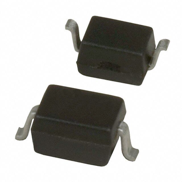
| 供应商器件封装 | SOD-323 |
| 其它名称 | F6270CT |
| 击穿电压 | 3.5 V |
| 功率-峰值脉冲 | 750W |
| 包装 | 剪切带 (CT) |
| 单向通道 | 1 |
| 双向通道 | - |
| 商标 | Littelfuse |
| 商标名 | SPA |
| 外壳高度 | 0.9 mm |
| 安装类型 | 表面贴装 |
| 安装风格 | SMD/SMT |
| 封装 | Reel |
| 封装/外壳 | SC-76,SOD-323 |
| 封装/箱体 | SOD-323 |
| 尺寸 | 1.4 mm W x 2.7 mm L x 1 mm H |
| 峰值浪涌电流 | 30 A |
| 峰值脉冲功率耗散 | 750 W |
| 工作温度 | -40°C ~ 125°C (TJ) |
| 工作电压 | 3.3 V |
| 工厂包装数量 | 3000 |
| 应用 | 通用 |
| 最大工作温度 | + 125 C |
| 最小工作温度 | - 40 C |
| 极性 | Unidirectional |
| 标准包装 | 1 |
| 特色产品 | http://www.digikey.cn/product-highlights/zh/sp4020-and-sp4021-series-tvs-diode-arrays/52463 |
| 电压-击穿(最小值) | 3.5V |
| 电压-反向关态(典型值) | 3.3V (最小值) |
| 电压-箝位(最大值)@Ipp | 21.8V (标准) |
| 电容 | 2.5 pF |
| 电流-峰值脉冲(10/1000µs) | 24A (8/20µs) |
| 电源线路保护 | 无 |
| 端接类型 | SMD/SMT |
| 类型 | 齐纳 |
| 系列 | SP4021 |
| 通道 | 1 Channel |
| 钳位电压 | 21.8 V |


- 商务部:美国ITC正式对集成电路等产品启动337调查
- 曝三星4nm工艺存在良率问题 高通将骁龙8 Gen1或转产台积电
- 太阳诱电将投资9.5亿元在常州建新厂生产MLCC 预计2023年完工
- 英特尔发布欧洲新工厂建设计划 深化IDM 2.0 战略
- 台积电先进制程称霸业界 有大客户加持明年业绩稳了
- 达到5530亿美元!SIA预计今年全球半导体销售额将创下新高
- 英特尔拟将自动驾驶子公司Mobileye上市 估值或超500亿美元
- 三星加码芯片和SET,合并消费电子和移动部门,撤换高东真等 CEO
- 三星电子宣布重大人事变动 还合并消费电子和移动部门
- 海关总署:前11个月进口集成电路产品价值2.52万亿元 增长14.8%


PDF Datasheet 数据手册内容提取
TVS Diode Array (SPA ® Diodes) Lightning Surge Protection- SP4020 Series SP4020 Series 2.5pF, 30A Discrete TVS Diode RoHS Pb GREEN Description The SP4020 components integrate low capacitance steering diodes with one or two avalanche breakdown diodes for unidirectional or bidirectional protection, respectively, to protect against ESD and lightning induced surge events. These devices can safely absorb up to 30A per IEC 61000-4-5 (tp=8/20μs) without performance degradation and a minimum ±30kV ESD per IEC 61000- 4-2 International Standard. The low loading capacitance and high surge capability make it ideal for protecting telecommunication ports such as Ethernet and other high speed data interfaces. Pinout Features • ESD, IEC 61000-4-2, Bidirectional configuration ±30kV contact, ±30kV air • Small SOD323 package 1 • EFT, IEC 61000-4-4, 40A fits 0805 footprints (5/50ns) • Moisture Sensitivity Level • Lightning, 30A (8/20 as (MSL-1) defined in IEC 61000-4-5 • AEC-Q101 Qualified 2nd edition) • Halogen free, Lead free, • Low capacitance of 2.5pF and RoHS compliant (@ V =0V) R • Low leakage current of 0.1μA at 3.3V • Unidirectional and 2 Functional Block Diagram Applications 1 1 •10/100/1000 Ethernet •Power Ports •T1/E1/T3/E3 •Computers and Peripherals •USB 1.1/2.0 •Instrumentation •USB 3.0/3.1 •Medical Equipment Additional Information 2 2 Unidirectional Bidirectional SP4020-01FTG SP4020-01FTG-C Datasheet Resources Samples Life Support Note: Not Intended for Use in Life Support or Life Saving Applications The products shown herein are not designed for use in life sustaining or life saving applications unless otherwise expressly indicated. ©2018 Littelfuse, Inc. Specifications are subject to change without notice. Revision: 12/12/18
TVS Diode Array (SPA ® Diodes) Lightning Surge Protection- SP4020 Series Absolute Maximum Ratings Symbol Parameter Value Units I Peak Current (t=8/20μs) 30 A PP p P Peak Pulse Power (t=8/20μs) 750 W Pk p T Operating Temperature -40 to 125 °C OP T Storage Temperature -55 to 150 °C STOR Note: CAUTION: Stresses above those listed in “Absolute Maximum Ratings” may cause permanent damage to the component. This is a stress only rating and operation of the component at these or any other conditions above those indicated in the operational sections of this specification is not implied. Electrical Characteristics (T =25ºC) OP Parameter Symbol Test Conditions Min Typ Max Units Breakdown Voltage V I =2uA 3.5 V BR R Reverse Standoff Voltage V I =1μA 3.3 V RWM R Reverse Leakage Current I V =3.3V 0.1 0.5 μA LEAK R I =1A, t=8/20µs, Fwd 6.6 V PP p Clamp Voltage1 V I =10A, t=8/20µs, Fwd 14.2 V C PP p I =24A, t=8/20μs, Fwd 21.8 V PP P Dynamic Resistance2 R TLP, t =100ns, I/O to GND 0.40 Ω DYN P IEC 61000-4-2 (Contact Discharge) ±30 kV ESD Withstand Voltage1 V ESD IEC 61000-4-2 (Air Discharge) ±30 kV Diode Capacitance1 C Reverse Bias=0V, f=1MHz 2.5 pF D Note: 1Parameter is guaranteed by design and/or component characterization. 2Transmission Line Pulse (TLP) with 100ns width and 200ps rise time. Normalized Capacitance vs. Bias Voltage 1.4 SP4020-01FTG-C SP4020-01FTG 1.2 e nc 1.0 a pacit 0.8 a C ed 0.6 aliz m 0.4 or N 0.2 0.0 0.0 0.3 0.6 0.9 1.2 1.5 1.8 2.1 2.4 2.7 3.0 3.3 Bias Voltage (V) ©2018 Littelfuse, Inc. Specifications are subject to change without notice. Revision: 12/12/18
TVS Diode Array (SPA ® Diodes) Lightning Surge Protection- SP4020 Series Positive Transmission Line Pulsing (TLP) Plot NegativeTransmission Line Pulsing (TLP) Plot 20 0 18 -2 -4 16 -6 TLP Current (A)1118024 TLP Current (A)--11-820 -14 6 -16 4 -18 2 -20 0 -15 -12 -9 -6 -3 0 0 3 6 9 12 15 TLP Voltage (V) TLP Voltage (V) Clamping Voltage vs. I 8/20 Pulse Waveform PP 110% 30.0 100% 25.0 90% V)C 80% amp Voltage ( 112050...000 Percent of IPP45670000%%%% Cl 30% 5.0 20% 0.0 10% 1.0 5.0 10.0 15.0 20.0 25.0 30.0 0% 0.0 5.0 10.0 15.0 20.0 25.0 30.0 Peak Pulse Current-IPP (A) Time (μs) ©2018 Littelfuse, Inc. Specifications are subject to change without notice. Revision: 12/12/18
TVS Diode Array (SPA ® Diodes) Lightning Surge Protection- SP4020 Series Soldering Parameters Product Characteristics Lead Plating Matte Tin Reflow Condition Pb – Free assembly Lead Material Alloy 42 - Temperature Min (T ) 150°C s(min) Lead Coplanarity 0.0004 inches (0.102mm) Pre Heat - Temperature Max (T ) 200°C s(max) - Time (min to max) (t) 60 – 180 secs Substrate Material Silicon s Average ramp up rate (Liquidus) Temp 3°C/second max Body Material Molded Compound (T) to peak L UL Recognized compound meeting TS(max) to TL - Ramp-up Rate 3°C/second max Flammability flammability rating V-0 - Temperature (T) (Liquidus) 217°C Reflow L - Temperature (t) 60 – 150 seconds L Peak Temperature (T) 260+0/-5 °C P Time within 5°C of actual peak 20 – 40 seconds Temperature (t) p Ramp-down Rate 6°C/second max Time 25°C to peak Temperature (T) 8 minutes Max. P Do not exceed 260°C tP TP CCrriittiiccaall ZZoonnee e RRaammpp--uupp TTLL ttoo TTPP rutare TS(mTaxL) tL pm RRaammpp--ddoown e PPrreehheeaatt T TS(min) tS 25 time to peak temperature Time ©2018 Littelfuse, Inc. Specifications are subject to change without notice. Revision: 12/12/18
TVS Diode Array (SPA ® Diodes) Lightning Surge Protection- SP4020 Series Part Marking System Part Numbering System SP4020-01FTG SP4020–01 F T G C Blank= Unidirectional C= Bidirectional 1 03 2 G= Green TVS Diode Arrays (SPA® Diodes ) T= Tape & Reel Series Package Number of F: SOD323 Channels SP4020-01FTG-C 1 3C 2 Ordering Information Part Number Package Min. Order Qty. SP4020-01FTG SOD323 3000 SP4020-01FTG-C SOD323 3000 Package Dimensions -SOD323 E A1 A2 SOD323 Symbol Millimeters Inches Min Max Min Max b D A 0.8 1.00 0.031 0.039 A1 0.00 0.10 0.000 0.004 A2 0.80 0.90 0.031 0.035 E1 A b 0.25 0.35 0.010 0.014 c 0.08 0.15 0.003 0.006 L 2 L1 Recommended Solder Pad .0 L D 1.20 1.40 0.047 0.055 0.49 1.79 E 1.60 1.80 0.063 0.071 5 4 c 0. 1.14 E1 2.50 2.75 0.098 0.108 2.28 L1 0.22 0.40 0.009 0.016 2.77 Unit: mm Embossed Carrier Tape & Reel Specification — SOD323 Symbol Millimeters A0 1.46+/-0.10 B0 2.90+/-0.10 W 8.0+0.3/-0.10 D0 1.50+0.10 D1 0.45min/1.15max E1 1.75+/-0.10 ,Ref. E2 - ,Ref. F 3.50+/-0.10 Component Orientation in Tape P0 4.00+/-0.10 P 4.00+/-0.10 P1 2.00+/-0.05 K0 1.25+/-0.10 T 0.254+/-0.02 ,Ref. 8mm TAPE AND REEL Pin1 ©2018 Littelfuse, Inc. Specifications are subject to change without notice. Revision: 12/12/18