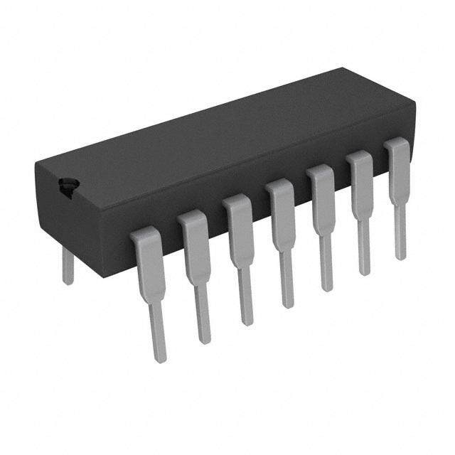
ICGOO在线商城 > 集成电路(IC) > 接口 - 驱动器,接收器,收发器 > SP3495EEN-L
- 型号: SP3495EEN-L
- 制造商: Exar
- 库位|库存: xxxx|xxxx
- 要求:
| 数量阶梯 | 香港交货 | 国内含税 |
| +xxxx | $xxxx | ¥xxxx |
查看当月历史价格
查看今年历史价格
SP3495EEN-L产品简介:
ICGOO电子元器件商城为您提供SP3495EEN-L由Exar设计生产,在icgoo商城现货销售,并且可以通过原厂、代理商等渠道进行代购。 SP3495EEN-L价格参考。ExarSP3495EEN-L封装/规格:接口 - 驱动器,接收器,收发器, 半 收发器 1/1 RS422,RS485 8-SOIC。您可以下载SP3495EEN-L参考资料、Datasheet数据手册功能说明书,资料中有SP3495EEN-L 详细功能的应用电路图电压和使用方法及教程。
| 参数 | 数值 |
| 产品目录 | 集成电路 (IC)半导体 |
| 描述 | IC TXRX RS485/RS422 ESD 8NSOICRS-422/RS-485 接口 IC Half Duplex RS-422/ RS-485 Transceiver |
| 产品分类 | |
| 品牌 | Exar Corporation |
| 产品手册 | |
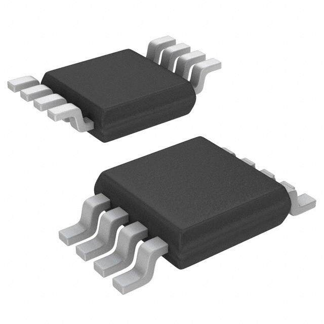
| 产品图片 |
|
| rohs | 符合RoHS无铅 / 符合限制有害物质指令(RoHS)规范要求 |
| 产品系列 | 接口 IC,RS-422/RS-485 接口 IC,Exar SP3495EEN-L- |
| 数据手册 | http://www.exar.com/Common/Content/Document.ashx?id=1387 |
| 产品型号 | SP3495EEN-L |
| PCN设计/规格 | |
| 产品种类 | RS-422/RS-485 接口 IC |
| 传播延迟时间ns | 24 ns, 40 ns |
| 供应商器件封装 | 8-SOIC N |
| 关闭 | Yes |
| 其它名称 | 1016-1151-5 |
| 功能 | Transceiver |
| 包装 | 管件 |
| 协议 | RS422,RS485 |
| 双工 | 半 |
| 商标 | Exar |
| 安装类型 | 表面贴装 |
| 安装风格 | SMD/SMT |
| 封装/外壳 | 8-SOIC(0.154",3.90mm 宽) |
| 封装/箱体 | SOIC-8 Narrow |
| 工作温度 | -40°C ~ 85°C |
| 工作温度范围 | - 40 C to + 85 C |
| 工作电源电压 | 3.3 V |
| 工厂包装数量 | 48 |
| 接收器滞后 | 25mV |
| 接收机数量 | 1 Receiver |
| 数据速率 | 32Mbps |
| 最大工作温度 | + 85 C |
| 最小工作温度 | - 40 C |
| 标准包装 | 48 |
| 激励器数量 | 1 Driver |
| 电压-电源 | 3 V ~ 3.6 V |
| 电源电流 | 5 mA |
| 类型 | 收发器 |
| 驱动器/接收器数 | 1/1 |


- 商务部:美国ITC正式对集成电路等产品启动337调查
- 曝三星4nm工艺存在良率问题 高通将骁龙8 Gen1或转产台积电
- 太阳诱电将投资9.5亿元在常州建新厂生产MLCC 预计2023年完工
- 英特尔发布欧洲新工厂建设计划 深化IDM 2.0 战略
- 台积电先进制程称霸业界 有大客户加持明年业绩稳了
- 达到5530亿美元!SIA预计今年全球半导体销售额将创下新高
- 英特尔拟将自动驾驶子公司Mobileye上市 估值或超500亿美元
- 三星加码芯片和SET,合并消费电子和移动部门,撤换高东真等 CEO
- 三星电子宣布重大人事变动 还合并消费电子和移动部门
- 海关总署:前11个月进口集成电路产品价值2.52万亿元 增长14.8%



PDF Datasheet 数据手册内容提取
SP3495E-3497E HIGH SPEED +3.3V RS-485/RS-422 TRANSCEIVERS WITH +/-15KV ESD PROTECTION AND ADVANCED FAILSAFE MAY 2009 REV. 1.0.0 GENERAL DESCRIPTION and outputs are ESD protected up to +/-15kV Human Body Model. The SP3495E - SP3497E transceivers are suitable for high speed bidirectional communication on FEATURES multipoint bus transmission lines. They are designed for balanced data transmission and comply with both • 3.3V Single Supply Operation RS-485 and RS-422 EIA standards. Each device • High Speed up to 32Mbps contains one differential driver and one differential receiver • Robust +/-15kV ESD protection Driver differential outputs and receiver differential • Hot Swap glitch protection inputs are connected internally to form a half-duplex • Advanced Fail-safe Receiver Inputs input/output to the RS-485 bus. Separate RE and DE pins enable and disable the driver and receiver • Half Unit Load, 64 Transceivers on bus independently or may be externally connected • Driver short circuit current limit and thermal together as a direct control. The device enters a low shutdown for overload protection power shutdown mode if both driver and receiver are disabled. the bus-pin outputs of disabled or powered • Low Current 1uA shutdown mode down devices are in high impedance state. The high TYPICAL APPLICATIONS impedance driver output is maintained over the entire common-mode voltage range of -7V to +12V. • Factory Automation Controls SP3495E - SP3497E operates from a single 3.3V • Motor Control power supply. SP3495E - SP3497E transceivers load the data bus only half as much as a standard RS-485 • Industrial Process Control unit load. This allows up to 64 devices to be • Building Automation connected simultaneously on a bus without violating required RS-485 signal margin and without using • Security Systems repeaters. Excessive power dissipation caused by • Remote Utility Meter Reading bus contention or by shorting outputs to ground or a voltage source is prevented by short circuit protection • Long or un-terminated transmission lines and thermal shutdown. This feature forces the driver output into high impedance state if the absolute value of the output current exceeds 250mA or if junction temperature exceeds 165°C. Receivers will fail-safe to a logic high output state if the inputs are unconnected (floating) or shorted. All RS-485 inputs FIGURE 1. TYPICAL APPLICATION CIRCUIT Exar Corporation 48720 Kato Road, Fremont CA, 94538 • (510) 668-7000 • FAX (510) 668-7017 • www.exar.com
SP3495E-3497E HIGH SPEED +3.3V RS-485/RS-422 TRANSCEIVERS WITH +/-15KV ESD PROTECTION AND ADVANCED FAILSAFE REV. 1.0.0 FIGURE 2. PIN OUT ASSIGNMENT SP3495E 8-Pin Half Duplex 8 1 VCC RO R 2 7 RE B DE 3 6 A 4 DI D 5 GND SP3496E 8-pin Full Duplex 1 Vcc 2 8 A R R 7 B 6 3 Z D D 4 5 Y GND SP3497E 14-pin Full Duplex 1 14 Vcc NC 13 NC 2 12 A R R 11 B 3 RE 4 DE 10 Z 5 D D 6 9 Y GND GND 7 8 NC ORDERING INFORMATION OPERATING TEMPERATURE PART NUMBER PACKAGE DEVICE STATUS RANGE SP3495EEN-L 8-pin Narrow SOIC -40°C to +85°C Active SP3495EEN-L/TR 8-pin Narrow SOIC -40°C to +85°C Active SP3496EEN-L 8-pin Narrow SOIC -40°C to +85°C Active SP3496EEN-L/TR 8-pin Narrow SOIC -40°C to +85°C Active SP3497EEN-L 14-pin Narrow SOIC -40°C to +85°C Active SP3497EEN-L/TR 14-pin Narrow SOIC -40°C to +85°C Active Note: To order Tape and Reel option include "/TR" in ordering part number. All packages are Pb-free/ RoHS compliant. 2
SP3495E-3497E REV. 1.0.0 HIGH SPEED +3.3V RS-485/RS-422 TRANSCEIVERS WITH +/-15KV ESD PROTECTION AND ADVANCED FAILSAFE PIN DESCRIPTIONS Pin Assignments PIN NUMBER PIN NAME TYPE DESCRIPTION HALF DUPLEX FULL DUPLEX SP3495E SP3496E SP3497E Receiver Output. When RE is low and if (A- 1 2 2 RO O B) ≥ -40mV, RO is High. If (A-B) ≤ -200mV, RO is Low. Receiver Output Enable, When RE is Low, RO is enabled. When RE is High, RO is 2 - 3 RE I high impedance. RE should be High and DE should be low to enter shutdown mode. RE is a hot-swap input. Driver Output Enable. When DE is High, outputs are enabled. When DE is low, out- 3 - 4 DE I puts are high impedance. DE should be low and RE should be High to enter shutdown mode. DE is a hot-swap input Driver Input. With DE high, a low level on DI forces Non-Inverting output low and invert- 4 3 5 DI I ing output high. Similarly, a high level on DI forces Non-Inverting output High and Invert- ing output Low. 5 4 6, 7 GND Pwr Ground Non-Inverting Receiver Input and Non- 6 - - A O Inverting Driver Output Inverting Receiver Input and Inverting 7 - - B O Driver Output +3.3V power supply input. Bypass with 8 1 14 Vcc Pwr 0.1uF capacitor. - 8 12 A I Non-Inverting Receiver Input - 7 11 B I Inverting Reciever Input - 5 9 Y O Non-Inverting Driver Output - 6 10 Z O Inverting Driver Output - - 1, 8, 13 NC - No Connect, not internally connected Pin type: I=Input, O=Output. 3
SP3495E-3497E HIGH SPEED +3.3V RS-485/RS-422 TRANSCEIVERS WITH +/-15KV ESD PROTECTION AND ADVANCED FAILSAFE REV. 1.0.0 ABSOLUTE MAXIMUM RATINGS These are stress ratings only and functional operation of the device at these ratings or any other above those indicated in the operation sections to the specifications below is not implied. Exposure to absolute maximum rating conditions for extended periods of time may affect reliability and cause permanent damage to the device. V +6.0V CC Input Voltage at control pins (RE, DE and DI) -0.5V to (V + 0.3V) CC Voltage Range on A and B pins -9V to +14V Storage Temperature Range -65°C to + 150°C Power Dissipation Maximum Junction Temperature 150°C 8-Pin SO θ = 128.4°C/W JA 14-Pin SO θ = 86°C/W JA CAUTION: ESD (Electrostatic Discharge) sensitive device. Permanent damage may occur on unconnected devices subject to high energy electrostatic fields. Unused devices must be stored in conductive foam or shunts. Personnel should be properly grounded prior to handling this device. The protective foam should be discharged to the destination socket before devices are removed. ELECTRICAL CHARACTERISTICS UNLESS OTHERWISE NOTED: VCC = +3.0V TO +3.6V WITH TA FROM -40OC TO +85OC. TYPICAL VALUES ARE AT VCC = +3.3V AND 25OC. SYMBOL PARAMETERS MIN. TYP. MAX. UNITS CONDITIONS DRIVER DC CHARACTERISTICS V Differential Driver Output Vcc V No Load OD 2.0 R = 100Ω (RS-422), Figure 3 L 1.5 R = 54Ω (RS-485), Figure 3 L 1.5 V = -7V, Figure 4 CM 1.5 V = +12V, Figure 4 CM ∆V Change in Magnitude of Differential -0.20 0.20 V R = 100Ω (RS-422), Figure 3, OD L Output See note 1 -0.20 0.20 R = 54Ω (RS-485), Figure 3, L See note 1 -0.20 0.20 V = -7V, Figure 4, See CM note 1 -0.20 0.20 V = +12V, Figure 4, See note CM 1 V Driver Common Mode Output 1.3 2.5 V Figure 3 OC Voltage steady state ∆V Change in Magnitude of Common -0.2 0.2 V Figure 3, See note 1 OC Mode Output Voltage I Driver Short Circuit Current Limit -250 mA V Forced to -7V, Figure 5 DSC OUT 250 mA V Forced to +12V, Figure 5 OUT 4
SP3495E-3497E REV. 1.0.0 HIGH SPEED +3.3V RS-485/RS-422 TRANSCEIVERS WITH +/-15KV ESD PROTECTION AND ADVANCED FAILSAFE UNLESS OTHERWISE NOTED: VCC = +3.0V TO +3.6V WITH TA FROM -40OC TO +85OC. TYPICAL VALUES ARE AT VCC = +3.3V AND 25OC. SYMBOL PARAMETERS MIN. TYP. MAX. UNITS CONDITIONS V 2.0 V Logic Input High IH Logic Input Thresholds (DI, DE, RE) V 0.8 V Logic Input Low IL V Driver Input Hysteresis 100 mV T = 25°C HYS A I Logic Input Current (DI, DE and RE) 10 uA IN = 0V IN -10 uA IN = Vcc Driver AC Characteristics freq Data Signaling Rate 32 Mbps 1/t , Duty Cycle 40 to 60% UI t Driver Propagation Delay (low to 5 11 24 ns C = 50pF, R = 54Ω, PLH L L High) freq = 8MHz, Figures 6 and 7 t Driver Propagation Delay (High to 5 11 24 ns C = 50pF, R = 54Ω, PHL L L Low) freq = 8MHz, Figures 6 and 7 t Driver Rise Time 2.5 4.5 10 ns C = 50pF, R = 54Ω, R L L freq = 8MHz, Figures 6 and 7 t Driver Fall time 2.5 4.5 10 ns C = 50pF, R = 54Ω, F L L freq = 8MHz, Figures 6 and 7 |t t | Differential Pulse Skew 3 ns Figures 6 and 7 PLH-PHL t Driver Enable to Output High 50 ns C = 50pF, R = 500Ω, Figures OZH L L 8 and 9 t Driver Enable to Outut Low 50 ns C = 50pF, R = 500Ω, Figures OZL L L 10 and 11 t Driver Disable from Output High 50 ns C = 50pF, R = 500Ω, Figures OHZ L L 8 and 9 t Driver Disable from Output Low 50 ns C = 50pF, R = 500Ω, Figures OLZ L L 10 and 11 t Shutdown to Driver Output Valid 6 us C = 50pF, R = 500Ω OZV L L t Time to Shutdown 50 600 ns Note 2 and 3 SHDN RECEIVER DC CHARACTERISTICS I Input Current (A, B pins) -290 500 uA DE = 0, Vcc = 0 or 3.3V IN V or V = 12V, other input 0V A B V or V = -7V, other input 0V A B VIH Receiver Differential Thresholds -85 -40 mV -7V ≤ VCM ≤ 12V, rising (V - V ) A B VIL -200 -125 mV -7V ≤ VCM ≤ 12V, falling Receiver Input Hysteresis 25 mV V = 0V CM V Receiver Output Voltage High 2.4 V I = -8mA, V = 200mV OH OUT ID V Receiver Output Voltage Low 0.4 V I = 8mA, V = -200mV OL OUT ID 5
SP3495E-3497E HIGH SPEED +3.3V RS-485/RS-422 TRANSCEIVERS WITH +/-15KV ESD PROTECTION AND ADVANCED FAILSAFE REV. 1.0.0 UNLESS OTHERWISE NOTED: VCC = +3.0V TO +3.6V WITH TA FROM -40OC TO +85OC. TYPICAL VALUES ARE AT VCC = +3.3V AND 25OC. SYMBOL PARAMETERS MIN. TYP. MAX. UNITS CONDITIONS I High-Z Receiver Output Current -1 uA RE = Vcc, V = 0V OZ OUT 1 uA RE = Vcc, V = Vcc OUT I Receiver Output Short Circuit -95 mA V = 0V OSS OUT Current 95 mA V = Vcc OUT RIN Receiver Input Resistance 24 KΩ -7V ≤ VCM ≤ 12V RECEIVER AC CHARACTERISTICS freq Data Signaling Rate 32 Mbps 1/t , Duty Cycle 40 to 60% UI t Receiver Propagation Delay (Low to 15 40 ns V = +/-2V, C = 15pF, Freq = PLH ID L High) 8MHz, Figure 12 and 13 t Receiver Propagation Delay (High to 15 40 ns V = +/-2V, C = 15pF, Freq = PHL ID L Low) 8MHz, Figure 12 and 13 skew Receiver Propagation Delay Skew 3 ns V = +/-2V, C = 15pF, Freq = ID L 8MHz, Figure 12 and 13 skew = |t t | PLH-PHL t Receiver Output Rise Time 1 2 6 ns C = 15pF, Freq = 8MHz R L t Receiver Output Fall Time 1 2 6 ns C = 15pF, Freq = 8MHz F L t Receiver Enable to Output High 50 ns C = 15pF, R = 1kΩ, ZH L L Figure 14 t Receiver Enable to Output Low 50 ns C = 15pF, R = 1kΩ, ZL L L Figure 14 t Receiver Output High to Disable 50 ns C = 15pF, R = 1kΩ, HZ L L Figure 14 t Receiver Output Low to Disable 50 ns C = 15pF, R = 1kΩ, LZ L L Figure 14 t Shutdown to Receiver Output Valid 6 us C = 15pF, R = 1kΩ ZH(SHDN) L L High t Shutdown to Receiver Output Valid 6 us C = 15pF, R = 1kΩ ZL(SHDN) L L Low t Time to Shutdown 50 600 ns Note 2 and 3 SHDN POWER REQUIRMENTS AND RECOMMENDED OPERATING CONDITIONS Vcc Supply Voltage 3.0 3.3 3.6 V I Supply Current - Driver Enabled 5.0 mA DE = Vcc, No Load, RE and DI CC1 = 0V or Vcc I Supply Current - Receiver Enabled 5.0 mA DE = 0V, RE = 0V, No Load CC2 I Supply Current - Shutdown Mode 1 6 uA DE = 0V, RE = Vcc, DI = Vcc or CC3 0V T Thermal Shutdown Temperature 165 °C SD 6
SP3495E-3497E REV. 1.0.0 HIGH SPEED +3.3V RS-485/RS-422 TRANSCEIVERS WITH +/-15KV ESD PROTECTION AND ADVANCED FAILSAFE UNLESS OTHERWISE NOTED: VCC = +3.0V TO +3.6V WITH TA FROM -40OC TO +85OC. TYPICAL VALUES ARE AT VCC = +3.3V AND 25OC. SYMBOL PARAMETERS MIN. TYP. MAX. UNITS CONDITIONS Thermal Shutdown Hysteresis 20 °C ESD Protection at Pins A, B, Y and Z +/-15 kV Human Body Model NOTE: 1. Change in Magnitude of Differential Output Voltage and Change in Magnitude of Common Mode Output Voltage are the changes in output voltage when DI input changes state. 2. The transceivers are put into shutdown by bringing RE High and DE Low simultaneously for at least 600ns. If the control inputs are in this state for less than 50ns, the device is guaranteed not enter shutdown. If the enable inputs are held in this state for at least 600ns the device is assured to be in shutdown. Note that the receiver and driver enable times increase during shutdown 3. Gauranteed by design and bench characterization. 7
SP3495E-3497E HIGH SPEED +3.3V RS-485/RS-422 TRANSCEIVERS WITH +/-15KV ESD PROTECTION AND ADVANCED FAILSAFE REV. 1.0.0 FIGURE 3. DRIVER DC TEST CIRCUIT R/2 DI D VOD R/2 VOC VCC FIGURE 4. DRIVER COMMON MODE LOAD TEST DE = 3.3V 375Ω A/Y DI = 0 or Vcc D VOD 60Ω B/Z 375Ω V CM FIGURE 5. DRIVER SHORT CIRCUIT CURRENT LIMIT TEST DE = 0 or Vcc A/Y IOS D DI = 0 or Vcc D 100Ω B/Z -7V to +12V V 8
SP3495E-3497E REV. 1.0.0 HIGH SPEED +3.3V RS-485/RS-422 TRANSCEIVERS WITH +/-15KV ESD PROTECTION AND ADVANCED FAILSAFE FIGURE 6. DRIVER PROPAGATION DELAY TEST CIRCUIT R C Y L L 54Ω 50pF DI D VOD Z 3.3V FIGURE 7. DRIVER PROPAGATION DELAY TIMING DIAGRAM Vcc DI Vcc/2 Vcc/2 0V t t PLH PHL Z 1/2V 1/2V V O O O Y t t DPLH DPHL V + V O 90% 90% DIFF 0V VY – VZ VO– 10%tR 10%tF t = |t - t | SKEW DPLH DPHL FIGURE 8. DRIVER ENABLE AND DISABLE TIME TEST CIRCUIT 1 Y S1 DI 0 or Vcc D OUT Z R = 500Ω C = 50pF L L GENERATOR 50Ω 9
SP3495E-3497E HIGH SPEED +3.3V RS-485/RS-422 TRANSCEIVERS WITH +/-15KV ESD PROTECTION AND ADVANCED FAILSAFE REV. 1.0.0 FIGURE 9. DRIVER ENABLE DISABLE TIMING DIAGRAM 1 Vcc DE Vcc/2 0 t , t (SHDN) ZH ZH 0.25V OUT V = (V + Vcc)/2 OM OL 0 t HZ FIGURE 10. DRIVER ENABLE AND DISABLE TIME TEST CIRCUIT 2 Vcc R = 500Ω L Y S1 DI 0 or Vcc D OUT Z C = 50pF L GENERATOR 50Ω 10
SP3495E-3497E REV. 1.0.0 HIGH SPEED +3.3V RS-485/RS-422 TRANSCEIVERS WITH +/-15KV ESD PROTECTION AND ADVANCED FAILSAFE FIGURE 11. DRIVER ENABLE AND DISABLE TIMING DIAGRAM 2 Vcc Vcc/2 DE 0 t , t (SHDN) ZL ZL t LZ Vcc OUT V = (V + Vcc)/2 V OM OL 0.25V OL FIGURE 12. RECEIVER PROPAGATION DELAY TEST CIRCUIT A OUT VID R B C L 15pF RE FIGURE 13. RECEIVER PROPAGATION DELAY TIMING DIAGRAM A +1V B -1V t t PHL PLH V 1.5V OH OUT V OL 11
SP3495E-3497E HIGH SPEED +3.3V RS-485/RS-422 TRANSCEIVERS WITH +/-15KV ESD PROTECTION AND ADVANCED FAILSAFE REV. 1.0.0 FIGURE 14. RECEIVER ENABLE AND DISABLE TIMES TEST CIRCUIT S1 1.5V S3 B 1kΩ Vcc -1.5V A R S2 RE C= 15pF L GENERATOR 50Ω FIGURE 15. RECEIVER ENABLE AND DISABLE TIMING DIAGRAM 1 S1 is open, S2 is closed, S3 = 1.5V 3V 1.5V RE t t ZH, ZH(SHDN) V OH OUT V /2 OH 0V FIGURE 16. RECEIVER ENABLE AND DISABLE TIMING DIAGRAM 2 S1 is closed, S2 is open, S3 = -1.5V 3V 1.5V RE 0V t t ZL, ZL(SHDN) V CC OUT VOL = VCC/2 V OL 12
SP3495E-3497E REV. 1.0.0 HIGH SPEED +3.3V RS-485/RS-422 TRANSCEIVERS WITH +/-15KV ESD PROTECTION AND ADVANCED FAILSAFE FIGURE 17. RECEIVER ENABLE AND DISABLE TIMING DIAGRAM 3 S1 is open, S2 is closed, S3 = 1.5V 3V 1.5V RE t HZ 0.25V V OH OUT 0V FIGURE 18. RECEIVER ENABLE AND DISABLE TIMING DIAGRAM 4 S1 is closed, S2 is open, S3 = -1.5V 3V 1.5V RE 0V t LZ V CC OUT 0.25V V OL 13
SP3495E-3497E HIGH SPEED +3.3V RS-485/RS-422 TRANSCEIVERS WITH +/-15KV ESD PROTECTION AND ADVANCED FAILSAFE REV. 1.0.0 1.0 PRODUCT DESCRIPTION The SP349xE high speed transceivers contain one driver and one receiver. The SP3495 is a half-duplex design while the SP3496E and SP3497E are full-duplex designs. The control pins RE and DE feature a hotswap capability allowing live insertion without spurious data transfer. Drivers are output short-circuit current limited. Thermal-shutdown circuitry protects drivers against excessive power dissipation. When activited, the thermal-shutdown circuitry forces the driver outptus into a high-impedance state. Advanced Failsafe The Receivers incorporate fail-safe circuitry, which guarantees a logic-high receiver output when the receiver inputs are open or shorted, or when they are connected to a terminated transmission line with all drivers disabled. In a terminated bus with all transmitters disabled the receivers differential input voltage is pulled to 0V by the termination. The SP349xE interprets 0V differential as a logic high with a minimum 40mV noise margin. HOT-SWAP CAPABILITY When Vcc is first applied the SP349xE holds the driver enable and receiver enable inactive for approximately 10 microseconds. During power ramp-up other system IC’s may drive unpredictable values. Hot-swap capability prevents the SP349xE from driving any output signal until power has stabilized. After the initial power-up sequence, the hot-swap circuit becomes transparent and driver enable and receiver enable resume their normal functions and timings 14
SP3495E-3497E REV. 1.0.0 HIGH SPEED +3.3V RS-485/RS-422 TRANSCEIVERS WITH +/-15KV ESD PROTECTION AND ADVANCED FAILSAFE PACKAGE DIMENSIONS (14 PIN NSOIC) 15
SP3495E-3497E HIGH SPEED +3.3V RS-485/RS-422 TRANSCEIVERS WITH +/-15KV ESD PROTECTION AND ADVANCED FAILSAFE REV. 1.0.0 PACKAGE DIMENSIONS (8 PIN NSOIC) 16
SP3495E-3497E HIGH SPEED +3.3V RS-485/RS-422 TRANSCEIVERS WITH +/-15KV ESD PROTECTION AND ADVANCED FAILSAFE REV. 1.0.0 REVISION HISTORY DATE REVISION DESCRIPTION 5/01/09 1.0.0 Production Release. NOTICE EXAR Corporation reserves the right to make changes to the products contained in this publication in order to improve design, performance or reliability. EXAR Corporation assumes no responsibility for the use of any circuits described herein, conveys no license under any patent or other right, and makes no representation that the circuits are free of patent infringement. Charts and schedules contained here in are only for illustration purposes and may vary depending upon a user’s specific application. While the information in this publication has been carefully checked; no responsibility, however, is assumed for inaccuracies. EXAR Corporation does not recommend the use of any of its products in life support applications where the failure or malfunction of the product can reasonably be expected to cause failure of the life support system or to significantly affect its safety or effectiveness. Products are not authorized for use in such applications unless EXAR Corporation receives, in writing, assurances to its satisfaction that: (a) the risk of injury or damage has been minimized; (b) the user assumes all such risks; (c) potential liability of EXAR Corporation is adequately protected under the circumstances. Copyright 2009 EXAR Corporation Datasheet May 2009. Send your technical inquiries with details to our e-mail hotline: uarttechsupport@exar.com. Reproduction, in part or whole, without the prior written consent of EXAR Corporation is prohibited. 17

 Datasheet下载

