ICGOO在线商城 > 集成电路(IC) > 接口 - 驱动器,接收器,收发器 > SP3243EBCR-L
 Datasheet下载
- 型号: SP3243EBCR-L
- 制造商: Exar
- 库位|库存: xxxx|xxxx
- 要求:
| 数量阶梯 | 香港交货 | 国内含税 |
| +xxxx | $xxxx | ¥xxxx |
查看当月历史价格
查看今年历史价格
SP3243EBCR-L产品简介:
ICGOO电子元器件商城为您提供SP3243EBCR-L由Exar设计生产,在icgoo商城现货销售,并且可以通过原厂、代理商等渠道进行代购。 SP3243EBCR-L价格参考。ExarSP3243EBCR-L封装/规格:接口 - 驱动器,接收器,收发器, 全 收发器 3/5 RS232 32-QFN(5x5)。您可以下载SP3243EBCR-L参考资料、Datasheet数据手册功能说明书,资料中有SP3243EBCR-L 详细功能的应用电路图电压和使用方法及教程。
MaxLinear, Inc. 的型号 SP3243EBCR-L 属于接口类器件,具体为 RS-232 驱动器/接收器(即串口通信芯片)。该芯片广泛应用于需要串行通信的电子设备中,适用于工业控制、通信设备、测试仪器、嵌入式系统等领域。

SP3243EBCR-L 支持多协议通信,具备高数据传输速率和良好的抗干扰能力,适用于复杂电磁环境下的稳定通信需求。其典型应用场景包括:

1. 工业自动化设备:如PLC、人机界面(HMI)、传感器和执行器之间的串口通信。
2. 通信模块:用于路由器、交换机、无线基站等设备中,实现控制信号的串行传输。
3. 测试与测量仪器:如示波器、万用表等设备,常通过RS-232接口与计算机或其他设备进行数据交换。
4. 医疗设备:用于监护仪、分析仪器等设备中,实现设备间的数据传输与控制。
5. 嵌入式系统开发板:为嵌入式处理器提供标准串口通信接口,用于调试和数据传输。

该芯片采用小型封装,功耗低,适合在空间受限和对功耗敏感的应用中使用。
| 参数 | 数值 |
| 产品目录 | 集成电路 (IC)半导体 |
| 描述 | IC TXRX RS232 INTELLIGENT 32QFNRS-232接口集成电路 Intelligent 3-5.5V RS-232 Transceiver |
| 产品分类 | |
| 品牌 | Exar Corporation |
| 产品手册 | |
| 产品图片 |
|
| rohs | 符合RoHS无铅 / 符合限制有害物质指令(RoHS)规范要求 |
| 产品系列 | 接口 IC,RS-232接口集成电路,Exar SP3243EBCR-L- |
| 数据手册 | http://www.exar.com/Common/Content/Document.ashx?id=636 |
| 产品型号 | SP3243EBCR-L |
| PCN其它 | |
| 产品种类 | RS-232接口集成电路 |
| 传播延迟时间ns | 0.15 us |
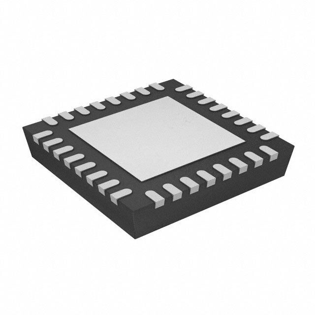
| 供应商器件封装 | 32-QFN 裸露焊盘(5x5) |
| 关闭 | Yes |
| 其它名称 | 1016-1118 |
| 功能 | Transceiver |
| 包装 | 托盘 |
| 协议 | RS232 |
| 双工 | 全 |
| 商标 | Exar |
| 安装类型 | 表面贴装 |
| 安装风格 | SMD/SMT |
| 封装/外壳 | 32-VFQFN 裸露焊盘 |
| 封装/箱体 | QFN-32 |
| 工作温度 | 0°C ~ 70°C |
| 工作温度范围 | - 40 C to + 85 C |
| 工作电源电压 | 3 V to 5.5 V |
| 接收器滞后 | 300mV |
| 接收机数量 | 5 Receiver |
| 数据速率 | 250kbps |
| 最大功率耗散 | 2.352 W |
| 最大工作温度 | + 85 C |
| 最小工作温度 | - 40 C |
| 标准包装 | 490 |
| 激励器数量 | 3 Driver |
| 电压-电源 | 3 V ~ 5.5 V |
| 电源电流 | 1 mA |
| 类型 | 收发器 |
| 输入/输出端数量 | 17 |
| 驱动器/接收器数 | 3/5 |

%20Renders/32-VQFN%20Exposed%20Pad.jpg)


PDF Datasheet 数据手册内容提取
SP3243E 3 Driver/5 Receiver Intelligent +3.0V to +5.5V RS-232 Transceivers FEATURES ■ Meets true EIA/TIA-232-F Standards C2+ 1 28 C1+ from a +3.0V to +5.5V power supply C2- 2 27 V+ ■ Interoperable with EIA/TIA-232 and V- 3 26 VCC adheres to EIA/TIA-562 down to a +2.7V R1IN 4 25 GND power source R2IN 5 24 C1- ■ AUTO ON-LINE® circuitry automatically R3IN 6 SP3243E 23 ONLINE wakes up from a 1µA shutdown ■ Regulated Charge Pump Yields Stable R4IN 7 22 SHUTDOWN RS-232 Outputs Regardless of V R5IN 8 21 STATUS Variations CC T1OUT 9 20 R2OUT ■ Enhanced ESD Specifications: T2OUT 10 19 R1OUT +15kV Human Body Model T3OUT 11 18 R2OUT +15kV IEC61000-4-2 Air Discharge T3IN 12 17 R3OUT +8kV IEC61000-4-2 Contact Discharge T2IN 13 16 R4OUT ■ 250 Kbps min. transmission rate (EB) T1IN 14 15 R5OUT ■ 1000 Kbps min. transmission rate (EU) ■ Ideal for High Speed RS-232 Applications Now Available in Lead Free Packaging DESCRIPTION The SP3243E products are 3 driver/5 receiver RS-232 transceiver solutions intended for portable or hand-held applications such as notebook and palmtop computers. The SP3243E includes one complementary receiver that remains alert to monitor an external device's Ring Indicate signal while the device is shutdown. The SP3243E and EB devices feature slew-rate limited outputs for reduced crosstalk and EMI. The "U" and "H" series are optimized for high speed with data rates up to 1Mbps, easily meeting the demands of high speed RS-232 applications. The SP3243E series uses an internal high-efficiency, charge-pump power supply that requires only 0.1µF capacitors in 3.3V operation. This charge pump and Exar's driver architecture allow the SP3243E series to deliver compliant RS-232 performance from a single power supply ranging from +3.0V to +5.5V. The AUTO ON-LINE® feature allows the device to automatically "wake-up" during a shutdown state when an RS-232 cable is con- nected and a connected peripheral is turned on. Otherwise, the device automatically shuts itself down drawing less than 1µA. SELECTION TABLE Device Power RS-232 RS-232 External Auto TTL # of Data ESD Supplies Drivers Receivers Components On-Line 3- Pins Rate Rating Circuitry State SP3243E +3.0V to +5.5V 3 5 4 Capacitors Yes Yes 28 120 15kV SP3243EB +3.0V to +5.5V 3 5 4 Capacitors Yes Yes 28 250 15kV SP3243EH +3.0V to +5.5V 3 5 4 Capacitors Yes Yes 28 460 15kV SP3243EU +3.0V to +5.5V 3 5 4 Capacitors Yes Yes 28 1000 15kV Exar Corporation 48720 Kato Road, Fremont CA, 94538 • 510-668-7017 • www.exar.com SP3243E_102_060611 1
ABSOLUTE MAXIMUM RATINGS These are stress ratings only and functional operation of the device at these ratings or any other above those indicated in the operation sections of the specifications below is not implied. Exposure to absolute maximum rating conditions for extended periods of time may affect reliability and cause permanent damage to the device. V .......................................................-0.3V to +6.0V Power Dissipation per package CC V+ (NOTE 1).......................................-0.3V to +7.0V 28-pin SOIC (derate 12.7mW/oC above +70oC).........1000mW V- (NOTE 1)........................................+0.3V to -7.0V 28-pin SSOP (derate 11.2mW/oC above +70oC)..........900mW V+ + |V-| (NOTE 1)...........................................+13V 28-pin TSSOP (derate 13.2mW/oC above +70oC)......1059mW I (DC V or GND current).........................+100mA 32-pin QFN (derate 29.4mW/oC above +70oC)...........2352mW CC CC Input Voltages TxIN, ONLINE,SHUTDOWN, .....-0.3V to Vcc +6.0V RxIN...................................................................+15V Output Voltages TxOUT.............................................................+13.2V RxOUT, STATUS.......................-0.3V to (V +0.3V) CC Short-Circuit Duration TxOUT....................................................Continuous Storage Temperature......................-65°C to +150°C NOTE 1: V+ and V- can have maximum magnitudes of 7V, but their absolute difference cannot exceed 13V. ELECTRICAL CHARACTERISTICS Unless otherwise noted, the following specifications apply for V = +3.0V to +5.5V with T = T to T , CC AMB MIN MAX C1 - C4 = 0.1µF. Typical values apply at V = +3.3V or +5.0V and T = 25°C. CC AMB PARAMETER MIN. TYP. MAX. UNITS CONDITIONS DC CHARACTERISTICS Supply Current, AUTO ON- 1.0 10 µA All RxIN open, ONLINE = GND, LINE® SHUTDOWN = V , V = 3.3V CC CC T = 25oC, TxIN = GND or V AMB CC Supply Current, Shutdown 1.0 10 µA SHUTDOWN = GND, VCC = 3.3V, T = 25oC, TxIN = Vcc or GND AMB Supply Current 0.3 1.0 mA ONLINE = SHUTDOWN = Vcc, no AUTO ON-LINE® Disabled load, V = 3.3V, T = +25oC, CC AMB TxIN = GND or V CC LOGIC INPUTS AND RECEIVER OUTPUTS Input Logic Threshold V = =3.3V or =5.0V, TxIN CC LOW 0.8 V ONLINE, SHUTDOWN HIGH 2.4 V Input Leakage Current +0.01 +1.0 µA TxIN, ONLINE, SHUTDOWN, T = +25oC, V = 0V to V AMB IN CC Output Leakage Current +0.05 +10 µA Receivers disabled, V = 0V to V OUT CC Output Voltage LOW 0.4 V I = 1.6mA OUT Output Voltage HIGH V -0.6 V -0.1 V I = -1.0mA CC CC OUT DRIVER OUTPUTS Output Voltage Swing +5.0 +5.4 V All driver outputs loaded with 3KΩ to GND, T = +25oC AMB Exar Corporation 48720 Kato Road, Fremont CA, 94538 • 510-668-7017 • www.exar.com SP3243E_102_060611 2
ELECTRICAL CHARACTERISTICS Unless otherwise noted, the following specifications apply for V = +3.0V to +5.5V with T = T to T , CC AMB MIN MAX C1 - C4 = 0.1µF. Typical values apply at V = +3.3V or +5.0V and T = 25°C. CC AMB PARAMETER MIN. TYP. MAX. UNITS CONDITIONS DRIVER OUTPUTS (continued) Output Resistance 300 Ω V = V+ = V- = 0V, V =+2V CC OUT Output Short-Circuit Current +35 +60 mA V = 0V OUT Output Leakage Current +25 µA V = 0V or 3.0V to 5.5V, V = CC OUT +12V, Drivers disabled RECEIVER INPUTS Input Voltage Range -15 15 V Input Threshold LOW 0.6 1.2 V Vcc = 3.3V Input Threshold LOW 0.8 1.5 V Vcc = 5.0V Input Threshold HIGH 1.5 2.4 V Vcc = 3.3V Input Threshold HIGH 1.8 2.4 V Vcc = 5.0V Input Hysteresis 0.3 V Input Resistance 3 5 7 kΩ AUTO ON-LINE® CIRCUITRY CHARACTERISTICS (ONLINE = GND, SHUTDOWN = VCC) 25°C STATUS Output Voltage LOW 0.4 V I = 1.6mA OUT STATUS Output Voltage HIGH V -0.6 V I = -1.0mA CC OUT Receiver Threshold to Drivers 350 µs Figure 14 Enabled (t ) ONLINE Receiver Positive or Negative 0.2 µs Figure 14 Threshold to STATUS HIGH (t ) STSH Receiver Positive or Negative 30 µs Figure 14 Threshold to STATUS LOW (t ) STSL TIMING CHARACTERISTICS Maximum Data Rate (U) 1000 Kbps R = 3KΩ, C = 250pF, one driver L L active (H) 460 R = 3KΩ, C = 1000pF, one L L driver active (B) 250 R = 3KΩ, C = 1000pF, one L L driver active ( - ) 120 R = 3KΩ, C = 1000pF, one L L driver active Receiver Propagation Delay t 0.15 µs Receiver input to Receiver out- PHL t 0.15 put, C = 150pF PLH L Receiver Output Enable Time 200 ns Normal operation Receiver Output Disable Time 200 ns Normal operation Driver Skew (E, EB) 100 500 ns | t - t | PHL PLH (EH, EU) 50 100 Receiver Skew 50 ns | t - t | PHL PLH Transition-Region Slew Rate Vcc = 3.3V, R = 3kΩ, T = L AMB (EH, EU) 90 V/µs 25°C, measurements taken from (E, EB) 6 30 -3.0V to +3.0V or +3.0V to -3.0V Exar Corporation 48720 Kato Road, Fremont CA, 94538 • 510-668-7017 • www.exar.com SP3243E_102_060611 3
TYPICAL PERFORMANCE CHARACTERISTICS Unless otherwise noted, the following performance characteristics apply for V = +3.3V, 1000kbps data rate, all CC drivers loaded with 3kΩ, 0.1µF charge pump capacitors, and T = +25°C. AMB 200 6 4 s) 150 put 2 Skew (n 10500 TTA12ll TaaXtt 53 l01o0.a2KdKebbdpp s3sK // CLoad Transmitter Out Voltage (V) --240 1OADltlh rDievrrei vDre arritvs e 1LrMsob aapdts e6d2 .w5iKthb p3sK // 250pF -6 0 2.7 3 3.5 4 4.5 5 0 250 500 1000 1500 2000 Supply Voltage (V) Load Capacitance (pF) Figure 1. Transmitter Skew VS. Load Capacitance Figure 2. Transmitter Output Voltage VS. Supply Voltage for the SP3243EU 40 6 35 Transmitterput Voltage (V)-2420 2M12b pTTsXX ’sa ta ftu1l/l1 d6a dta1a .tr5aaM treabtpes 1Mbps Current (mA) 32210505 250Kbps 120K2b0pKsbps Out-4 2Mbps 1.5Mbps 1Mbps Supply 105 12A lTTl rrTaarnnassnmmsmiittttieettrre sra sat tlfo u1all5 dD.5ea sKt a3b KRp sa+t eLoad Cap -6 0 0 250 500 1000 1500 2000 0 1000 2000 3000 4000 5000 Load Capacitance (pF) Load Capacitance (pF) Figure 3. Transmitter Output Voltage VS. Load Figure 4. Supply Current VS. Load Capacitance for Capacitance for the SP3243EU the SP3243EU 25 6 4 20 TxOUT + Supply Current (mA) 11505 12A lTTl rrdaarnnivssemmrsiitt ttloeearr sda eat dt2 15w50i.Kt6hbK 3pbKsp s// 1000pF Transmitter Output Voltage (V) --2420 TxOUT - 0 -6 2.7 3 3.5 4 4.5 5 0 1000 2000 3000 4000 5000 Supply Voltage (VDC) Load Capacitance (pF) Figure 5. Supply Current VS. Supply Voltage for the Figure 6. Transmitter Output Voltage VS. Load SP3243EU Capacitance for the SP3243EB Exar Corporation 48720 Kato Road, Fremont CA, 94538 • 510-668-7017 • www.exar.com SP3243E_102_060611 4
TYPICAL PERFORMANCE CHARACTERISTICS Unless otherwise noted, the following performance characteristics apply for V = +3.3V, 1000kbps data rate, all CC drivers loaded with 3kΩ, 0.1µF charge pump capacitors, and T = +25°C. AMB 25 20 - Slew µs) + Slew e (V/ 15 at R Slew 10 12 TTrraannssmmiitttteerr aatt 21550.6KKbbppss 5 All drivers loaded 3K + Load Cap 0 0 500 1000 2000 3000 4000 5000 Load Capacitance (pF) Figure 7. Slew Rate VS. Load Capacitance Exar Corporation 48720 Kato Road, Fremont CA, 94538 • 510-668-7017 • www.exar.com SP3243E_102_060611 5
PIN NUMBER NAME FUNCTION SP3243E SP3243EUCR QFN C1+ Positive terminal of the voltage doubler charge-pump capacitor 28 28 V+ Regulated +5.5V output generated by the charge pump 27 26 C1- Negative terminal of the voltage doubler charge-pump capacitor 24 22 C2+ Positive terminal of the inverting charge-pump capacitor 1 29 C2- Negative terminal of the inverting charge-pump capacitor 2 31 V- Regulated -5.5V output generated by the charge pump 3 32 RIN RS-232 receiver input. 4 2 1 RIN RS-232 receiver input 5 3 2 RIN RS-232 receiver input 6 4 3 RIN RS-232 receiver input 7 5 4 RIN RS-232 receiver input 8 6 5 ROUT TTL/CMOS receiver output 19 17 1 ROUT TTL/CMOS receiver output 18 16 2 ROUT Non-inverting receiver-2 output, active in shutdown 20 18 2 ROUT TTL/CMOS receiver output 17 15 3 ROUT TTL/CMOS receiver output 16 14 4 ROUT TTL/CMOS receiver output 15 13 5 STATUS TTL/CMOS Output indicating online and shutdown status 21 19 TIN TTL/CMOS driver input 14 12 1 TIN TTL/CMOS driver input 13 11 2 TIN TTL/CMOS driver input 12 10 3 ONLINE Apply logic HIGH to override AUTO ON-LINE® circuitry 23 21 keeping drivers acive (SHUTDOWN must also be logic HIGH, refer to Table 2) T1 RS-232 driver output 9 7 OUT T2 RS-232 driver output 10 8 OUT T3 RS-232 driver output 11 9 OUT GND Ground 25 23 V +3.0V to +5.5V supply voltage 26 25 CC SHUTDOWN Apply logic LOW to SHUTDOWN driver and charge pump. 22 20 This overrides all AUTO ON-LINE® circuitry and ONLINE (Refer to table 2) NC No Connection - 1,24,27,30 Table 1. Device Pin Description Exar Corporation 48720 Kato Road, Fremont CA, 94538 • 510-668-7017 • www.exar.com SP3243E_102_060611 6
VCC C5 +0.1µF 26 VCC + 28C1+ V+ 27 + C1 0.1µF C3 0.1µF 24C1- 1C2+ SP3243E V- 3 + C2 0.1µF C4 0.1µF 2C2- + 14T1IN T1OUT 9 TTL/CMOS 13T2IN T2OUT 10 RS-232 INPUTS 12T3IN T3OUT 11 OUTPUTS 20R2OUT 19R1OUT R1IN 4 5kΩ 18R2OUT R2IN 5 TTL/CMOS 5kΩ OUTPUTS 17R3OUT R3IN 6 RS-232 INPUTS 5kΩ 16R4OUT R4IN 7 5kΩ 15 R5OUT R5IN 8 VCC 22 5kΩ SHUTDOWN 23 ONLINE To µP SupCerirvcisuoitr 21STATUS GND 25 Figure 8. SP3243E Typical Operating Circuit V- C2- NC C2+ C1+ NC V+ VCC 2 1 0 9 8 7 6 5 3 3 3 2 2 2 2 2 NC 1 24 NC R1IN 2 23 GND R2IN 3 22 C1- R3IN 4 21 ONLINE SP3243E R4IN 5 20 SHUTDOWN R5IN 6 19 STATUS T1OUT 7 18 R2OUT T2OUT 8 17 R1OUT 9 10 11 12 13 14 15 16 T N N N T T T T U I I I U U U U O T3 T2 T1 O O O O T3 R5 R4 R3 R2 Figure 9. SP3243E QFN Pinout Configuration Exar Corporation 48720 Kato Road, Fremont CA, 94538 • 510-668-7017 • www.exar.com SP3243E_102_060611 7
DESCRIPTION In many portable or hand-held applications, an The SP3243E transceivers meet the EIA/TIA- RS-232 cable can be disconnected or a connected 232 and ITU-T V.28/V.24 communication protocols peripheral can be turned off. Under these condi- and can be implemented in battery-powered, tions, the internal charge pump and the drivers will portable, or hand-held applications such as be shut down. Otherwise, the system automati- notebook or palmtop computers. The SP3243E cally comes online. This feature allows design devices feature Exar's proprietary and patented engineers to address power saving concerns (U.S.-- 5,306,954) on-board charge pump cir- without major design changes. cuitry that generates ±5.5V RS-232 voltage levels from a single +3.0V to +5.5V power supply. The THEORY OF OPERATION SP3243EU devices can operate at a data rate The SP3243E series is made up of four basic of 1000kbps fully loaded. circuit blocks: 1. Drivers The SP3243E is a 3-driver/5-receiver device, 2. Receivers ideal for portable or hand-held applications. 3. the Exar proprietary charge pump, and The SP3243E includes one complementary 4. AUTO ON-LINE® circuitry. always-active receiver that can monitor an external device (such as a modem) in shutdown. Drivers This aids in protecting the UART or serial The drivers are inverting level transmitters that controller IC by preventing forward biasing convert TTL or CMOS logic levels to 5.0V EIA/ of the protection diodes where V may be CC TIA-232 levels with an inverted sense relative disconnected. to the input logic levels. Typically, the RS-232 output voltage swing is +5.4V with no load and +5V minimum fully loaded. The driver outputs are The SP3243E series is an ideal choice for power protected against infinite short-circuits to ground sensitive designs. The SP3243E devices feature without degradation in reliability. These drivers AUTO ON-LINE® circuitry which reduces the comply with the EIA-TIA-232-F and all previous power supply drain to a 1µA supply current. RS-232 versions. Unused drivers inputs should be connected to GND or V . CC VCC The drivers have a minimum data rate of 250kbps C5 +0.1µF VC2C6 (EB) or 1000kbps (EU) fully loaded. + 28C1+ V+ 27 + C1 0.1µF C3 0.1µF 24C1- 1C2+ SP3243E V- 3 Figure 11 shows a loopback test circuit used to C2 +0.1µF 2C2- C4 +0.1µF test the RS-232 Drivers. Figure 12 shows the TxD 14T1IN T1OUT 9 test results where one driver was active at 1Mbps RTS 13T2IN T2OUT10 ROSU-T2P3U2TS and all three drivers loaded with an RS-232 re- DTR 12T3IN T3OUT 11 UART 20R2OUT ceiver in parallel with a 250pF capacitor. Figure or RxD 19R1OUT R1IN 4 13 shows the test results of the loopback circuit Serial µC 5KΩ CTS 18R2OUT R2IN 5 with all drivers active at 250kbps with typical 5KΩ DSR 17R3OUT R3IN 6 RS-232 RS-232 loads in parallel with 1000pF capacitors. A DCD 16R4OUT 5KΩR4IN 7 INPUTS superior RS-232 data transmission rate of 1Mbps RI 15R5OUT 5KΩR5IN 8 makes the SP3243EU an ideal match for high VCC 22 5KΩ speed LAN and personal computer peripheral SHUTDOWN 23ONLINE applications. 21STATUS GND 25 RESET SupeµrPvisor VIN IC Figure 10. Interface Circuitry Controlled by Micropro- cessor Supervisory Circuit Exar Corporation 48720 Kato Road, Fremont CA, 94538 • 510-668-7017 • www.exar.com SP3243E_102_060611 8
+3V to +5V Device: SP3243E + C5 0.1µF VCC SHUTDOWN TxOUT RxOUT R2OUT + C1+ V+ + C1 0.1µF C3 0.1µF 0 High-Z High-Z Active C1- C2+ SP3243 V- 1 Active Active Active + C2 0.1µF C2- C4 +0.1µF T1IN T1OUT Table 2. SHUTDOWN Truth Tables TTLIN/CPMUOTSS TXIN TXOUT Nanodte S: HInU ATUDTOOW ONN -=L IVNE®, Mthoed dee wvhiceer ew OillN sLhINutE d =o GwNn Dif CC there is no activity present at the Receiver inputs. R1OUT R1IN 5KΩ TOTUL/TCPMUOTSS Receivers RXOUT RXIN 5KΩ The receivers convert +5.0V EIA/TIA-232 VCC 1000pF 1000pF levels to TTL or CMOS logic output levels. Re- SHUTDOWN ceivers are High-Z when the AUTO ON-LINE® ONLINE circuitry is enabled or when in shutdown. The To µP Supervisor STATUS Circuit GND truth table logic of the SP3243 driver and receiver 18 outputs can be found in Table 2. Figure 11. Loopback Test Circuit for RS-232 Driver Data Transmission Rates The SP3243E includes an additional non-in- verting receiver with an output ROUT. ROUT 2 2 is an extra output that remains active and monitors activity while the other receiver outputs are forced into high impedance. This allows a Ring Indicator (RI) signal from a peripheral to be monitored without forward biasing the TTL/CMOS inputs of the other devices connected to the receiver outputs. Since receiver input is usually from a transmis- sion line where long cable lengths and system interference can degrade the signal, the inputs have a typical hysteresis margin of 300mV. This ensures that the receiver is virtually immune to Figure 12. Loopback Test results at 1Mbps noisy transmission lines. Should an input be left unconnected, an internal 5KΩ pulldown resistor to ground will commit the output of the receiver to a HIGH state. Figure 13. Loopback Test results at 250Kbps Exar Corporation 48720 Kato Road, Fremont CA, 94538 • 510-668-7017 • www.exar.com SP3243E_102_060611 9
Charge Pump Phase 4 The charge pump is a Exar–patented design — V transfer — The fourth phase of the clock DD (U.S. 5,306,954) and uses a unique approach connects the negative terminal of C to GND, 2 compared to older less–efficient designs. and transfers this positive generated voltage The charge pump still requires four external across C to C, the V storage capacitor. This 2 4 DD capacitors, but uses a four–phase voltage voltage is regulated to +5.5V. At this voltage, shifting technique to attain symmetrical 5.5V the internal oscillator is disabled. Simultane- power supplies. The internal power supply ous with the transfer of the voltage to C, the 4 consists of a regulated dual charge pump that positive side of capacitor C is switched to V 1 CC provides output voltages 5.5V regardless of and the negative side is connected to GND, al- the input voltage (V ) over the +3.0V to +5.5V lowing the charge pump cycle to begin again. CC range. This is important to maintain compli- The charge pump cycle will continue as long ant RS-232 levels regardless of power supply as the operational conditions for the internal fluctuations. oscillator are present. The charge pump operates in a discontinuous Since both V+ and V– are separately generated mode using an internal oscillator. If the output from V , in a no–load condition V+ and V– will CC voltages are less than a magnitude of 5.5V, the be symmetrical. Older charge pump approaches charge pump is enabled. If the output voltages that generate V– from V+ will show a decrease in exceed a magnitude of 5.5V, the charge pump the magnitude of V– compared to V+ due to the is disabled. This oscillator controls the four inherent inefficiencies in the design. The clock phases of the voltage shifting. A description of rate for the charge pump typically operates at each phase follows. greater than 250kHz. The external capacitors can be as low as 0.1µF with a 16V breakdown Phase 1 voltage rating. — V charge storage — During this phase of the SS clock cycle, the positive side of capacitors C and 1 C are initially charged to V . C+ is then switched 2 CC l to GND and the charge in C– is transferred to C–. 1 2 Since C+ is connected to V , the voltage potential 2 CC across capacitor C is now 2 times V . 2 CC Phase 2 — V transfer — Phase two of the clock SS connects the negative terminal of C to the V 2 SS storage capacitor and the positive terminal of C to GND. This transfers a negative gener- 2 ated voltage to C. This generated voltage is 3 regulated to a minimum voltage of -5.5V. Simultaneous with the transfer of the voltage to C, 3 the positive side of capacitor C is switched to V 1 CC and the negative side is connected to GND. Phase 3 — V charge storage — The third phase of the DD clock is identical to the first phase — the charge transferred in C produces –V in the negative 1 CC terminal of C, which is applied to the negative 1 side of capacitor C. Since C+ is at V , the volt- 2 2 CC age potential across C is 2 times V . 2 CC Exar Corporation 48720 Kato Road, Fremont CA, 94538 • 510-668-7017 • www.exar.com SP3243E_102_060611 10
Minimum recommended charge pump capacitor value Input Voltage Vcc Charge pump capacitor value for SP32XX 3.0V to 3.6V C1 - C4 = 0.1µF 4.5V to 5.5V C1 = 0.047µF, C2 - C4 = 0.33µF 3.0V to 5.5V C1 - C4 = 0.22µF The Exar-patented charge pumps are designed reduces ripple on the transmitter outputs and to operate reliably with a range of low cost may slightly reduce power consumption. C2, capacitors. Either polarized or non polarized C3, and C4 can be increased without changing capacitors may be used. If polarized capacitors C1’s value. are used they should be oriented as shown in the Typical Operating Circuit. The V+ capaci- For best charge pump efficiency locate the tor may be connected to either ground or Vcc charge pump and bypass capacitors as close (polarity reversed.) as possible to the IC. Surface mount capacitors are best for this purpose. Using capacitors with The charge pump operates with 0.1µF capacitors lower equivalent series resistance (ESR) and for 3.3V operation. For other supply voltages, see self-inductance, along with minimizing parasitic the table for required capacitor values. Do not use PCB trace inductance will optimize charge pump values smaller than those listed. Increasing the operation. Designers are also advised to consider capacitor values (e.g., by doubling in value) that capacitor values may shift over time and operating temperature. AUTO ONLINE CIRCUITRY The SP3243E devices have a patent pending AUTO ON-LINE® circuitry on board that saves When the external transmitters are disabled or power in applications such as laptop computers, the cable is disconnected, the receiver inputs will palmtop (PDA) computers and other portable be pulled down by their internal 5kΩ resistors to systems. ground. When this occurs over a period of time, the internal transmitters will be disabled and the The SP3243E devices incorporate an AUTO device goes into a shutdown or standy mode. ON-LINE® circuit that automatically enables itself When ONLINE is HIGH, the AUTO ON-LINE® when the external transmitters are enabled and mode is disabled. the cable is connected. Conversely, the AUTO ON-LINE® circuit also disables most of the inter- The AUTO ON-LINE® circuit has two stages: nal circuitry when the device is not being used 1) Inactive Detection and goes into a standby mode where the device 2) Accumulated Delay typically draws 1µA. This function is externally controlled by the ONLINE pin. When this pin is tied to a logic LOW, the AUTO ON-LINE® function is active. Once active, the device is enabled until there is no activity on the receiver inputs. The receiver input typically sees at least +3V, which are generated from the transmitters at the other end of the cable with a +5V minimum. Exar Corporation 48720 Kato Road, Fremont CA, 94538 • 510-668-7017 • www.exar.com SP3243E_102_060611 11
S H U RECEIVER +2.7V T RS-232 INPUT 0V VOLTAGES -2.7V D O W VCC N STATUS 0V tSTSL tSTSH tONLINE +5V DRIVER RS-232 OUTPUT 0V VOLTAGES -5V Figure 14. AUTO ON-LINE® Timing Waveforms The first stage, shown in Figure 21, detects an The STATUS pin outputs a logic LOW signal inactive input. A logic HIGH is asserted on if the device is shutdown. This pin goes to a R INACT if the cable is disconnected or the logic HIGH when the external transmitters are X external transmitters are disabled. Otherwise, enabled and the cable is connected. R INACT will be at a logic LOW. This circuit is X duplicated for each of the other receivers. When the SP3243E devices are shut down, the charge pumps are turned off. V+ charge pump output decays to V , the V- output decays to The second stage of the AUTO ON-LINE® circuitry, CC GND. The decay time will depend on the size shown in Figure 22, processes all the receiver's of capacitors used for the charge pump. Once R INACT signals with an accumulated delay that X in shutdown, the time required to exit the shut disables the device to a 1µA supply current. down state and have valid V+ and V- levels is typically 200µs. The STATUS pin goes to a logic LOW when the cable is disconnected, the external transmit- For easy programming, the STATUS can be ters are disabled, or the SHUTDOWN pin is used to indicate DSR or a Ring Indicator sig- invoked. The typical accumulated delay is around nal. Tying ONLINE and SHUTDOWN together 20µs. will bypass the AUTO ON-LINE® circuitry so this connection acts like a shutdown input pin. When the SP3243E drivers or internal charge pump are disabled, the supply current is reduced to 1µA. This can commonly occur in hand-held or portable applications where the RS-232 cable is disconnected or the RS-232 drivers of the con- nected peripheral are turned off. The AUTO ON-LINE® mode can be disabled by the SHUTDOWN pin. If this pin is a logic LOW, the AUTO ON-LINE® function will not operate regardless of the logic state of the ONLINE pin. Table 3 summarizes the logic of the AUTO ON- LINE® operating modes. The truth table logic of the SP3243E driver and receiver outputs can be found in Table 2. Exar Corporation 48720 Kato Road, Fremont CA, 94538 • 510-668-7017 • www.exar.com SP3243E_102_060611 12
VCC = +5V +5V C4 + + + – VDD Storage Capacitor C1– C2– – + VSS Storage Capacitor –5V –5V C3 Figure 15. Charge Pump — Phase 1 VCC = +5V C4 + + + – VDD Storage Capacitor C1– C2– – + VSS Storage Capacitor -5.5V C3 Figure 16. Charge Pump — Phase 2 VCC = +5V +5V C4 + + + – VDD Storage Capacitor C1– C2– – + VSS Storage Capacitor –5V –5V C3 Figure 17. Charge Pump — Phase 3 VCC = +5V +5.5V C4 + + + – VDD Storage Capacitor C1– C2– – + VSS Storage Capacitor C3 Figure 18. Charge Pump — Phase 4 Exar Corporation 48720 Kato Road, Fremont CA, 94538 • 510-668-7017 • www.exar.com SP3243E_102_060611 13
The SP3243E driver outputs are able to maintain voltage under loading of up to 2.5mA per driver, 6 ensuring sufficient output for mouse-driving ap- plications. Voltage [V] 42 VVoouutt+- mitter Output -02 0.62 0.869 0.939 1.02 1.12 1.23 1.38 1.57 1.82 2.67 3.46 4.93 8.6 0 VOUT+ Trans -4 0 -6 Load Current PerTransmitter [mA] 1 VOUT- Figure 19. SP3243E Driver Output Voltages vs. Load Current per Transmitter VCC + 26 C5 0.1µF VCC + 28C1+ V+ 27 + C1 0.1µF C3 0.1µF 24C1- 1 C2+ SP3243E V- 3 + C2 0.1µF C4 0.1µF 2C2- + 14T1IN T1OUT 9 13T2IN T2OUT 10 12 T3IN T3OUT 11 20R2OUT 19R1OUT R1IN 4 5kΩ 18R2OUT R2IN 5 5kΩ 17 R3OUT R3IN 6 5kΩ 16 R4OUT R4IN 7 5kΩ 15 R5OUT R5IN 8 DB-9 Connector VCC 22 5kΩ SHUTDOWN 23 ONLINE 1 6 To µP SupCerirvcisuoitr 21 STATUS GND 7 2 3 25 8 4 9 5 DB-9 Connector Pins: 1. Received Line Signal Detector 6. DCE Ready 2. Received Data 7. Request to Send 3. Transmitted Data 8. Clear to Send 4. Data Terminal Ready 9. Ring Indicator 5. Signal Ground (Common) Figure 20. Circuit for the connectivity of the SP3243E with a DB-9 connector Exar Corporation 48720 Kato Road, Fremont CA, 94538 • 510-668-7017 • www.exar.com SP3243E_102_060611 14
RS-232SIGNAL SHUTDOWN TRANSCEIVER ATRECEIVER ONLINEINPUT STATUSOUTPUT INPUT STATUS INPUT YES HIGH LOW HIGH NormalOperation (Auto-Online) NO HIGH HIGH LOW NormalOperation Shutdown NO HIGH LOW LOW (Auto-Online) YES LOW HIGH / LOW HIGH Shutdown NO LOW HIGH / LOW LOW Shutdown Table 3. AUTO ON-LINE® Logic Inactive Detection Block RXINACT RS-232 RXIN Receiver Block RXOUT Figure 21. Stage I of AUTO ON-LINE® Circuitry Delay Delay Delay Delay Delay Stage Stage Stage Stage Stage STATUS R1INACT R2INACT R3INACT R4INACT R5INACT SHUTDOWN Figure 22. Stage II of AUTO ON-LINE® Circuitry Exar Corporation 48720 Kato Road, Fremont CA, 94538 • 510-668-7017 • www.exar.com SP3243E_102_060611 15
ESD TOLERANCE most of the ESD current when the ESD source is applied to the connector pins. The test circuit The SP3243E series incorporates ruggedized for IEC61000-4-2 is shown on Figure 24. There ESD cells on all driver output and receiver input are two methods within IEC61000-4-2, the Air pins. The ESD structure is improved over our Discharge method and the Contact Discharge previous family for more rugged applications method. and environments sensitive to electro-static dis- charges and associated transients. The improved With the Air Discharge Method, an ESD voltage ESD tolerance is at least +15kV without damage is applied to the equipment under test (EUT) nor latch-up. through air. This simulates an electrically charged person ready to connect a cable onto the rear of There are different methods of ESD testing ap- the system only to find an unpleasant zap just plied: before the person touches the back panel. The a) MIL-STD-883, Method 3015.7 b) IEC61000-4-2 Air-Discharge high energy potential on the person discharges c) IEC61000-4-2 Direct Contact through an arcing path to the rear panel of the system before he or she even touches the sys- The Human Body Model has been the generally tem. This energy, whether discharged directly accepted ESD testing method for semi-con- or through air, is predominantly a function of ductors. This method is also specified in the discharge current rather than the discharge MIL-STD-883, Method 3015.7 for ESD testing. voltage. Variables with an air discharge such as The premise of this ESD test is to simulate the approach speed of the object carrying the ESD human body’s potential to store electro-static potential to the system and humidity will tend to energy and discharge it to an integrated circuit. change the discharge current. For example, the The simulation is performed by using a test rise time of the discharge current varies with the model as shown in Figure 23. This method approach speed. will test the IC’s capability to withstand an ESD transient during normal handling such as in The Contact Discharge Method applies the ESD manufacturing areas where the ICs tend to be current directly to the EUT. This method was handled frequently. devised to reduce the unpredictability of the ESD arc. The discharge current rise time is constant The IEC-61000-4-2, formerly IEC801-2, is gen- since the energy is directly transferred without the erally used for testing ESD on equipment and air-gap arc. In situations such as hand held sys- systems. For system manufacturers, they must tems, the ESD charge can be directly discharged guarantee a certain amount of ESD protection to the equipment from a person already holding since the system itself is exposed to the outside the equipment. The current is transferred on to environment and human presence. The premise the keypad or the serial port of the equipment with IEC61000-4-2 is that the system is required directly and then travels through the PCB and to withstand an amount of static electricity when finally to the IC. ESD is applied to points and surfaces of the equipment that are accessible to personnel dur- ing normal usage. The transceiver IC receives RC RS SW1 SW2 Device DC Power CS Under Source Test Figure 23. ESD Test Circuit for Human Body Model Exar Corporation 48720 Kato Road, Fremont CA, 94538 • 510-668-7017 • www.exar.com SP3243E_102_060611 16
Contact-Discharge Model RC RS RV SW1 SW2 Device DC Power CS Under Source Test RS andRV add up to 330Ωfor IEC61000-4-2. Figure 24. ESD Test Circuit for IEC61000-4-2 The circuit models in Figures 23 and 24 represent the typical ESD testing circuit used for all three → I methods. The C is initially charged with the DC 30A S power supply when the first switch (SW1) is on. Now that the capacitor is charged, the second switch (SW2) is on while SW1 switches off. The voltage stored in the capacitor is then applied 15A through R , the current limiting resistor, onto the S device under test (DUT). In ESD tests, the SW2 switch is pulsed so that the device under test receives a duration of voltage. 0A t = 0ns t = 30ns For the Human Body Model, the current limiting t → resistor (R ) and the source capacitor (C ) are S S 1.5kΩ an 100pF, respectively. For IEC-61000-4-2, Figure 25. ESD Test Waveform for IEC61000-4-2 the current limiting resistor (R ) and the source ca- S pacitor (C ) are 330Ω an 150pF, respectively. S The higher C value and lower R value in the S S IEC61000-4-2 model are more stringent than the Human Body Model. The larger storage capaci- tor injects a higher voltage to the test point when SW2 is switched on. The lower current limiting resistor increases the current charge onto the DEVICE PIN HUMAN BODY IEC61000-4-2 TESTED MODEL Air Discharge Direct Contact Level Driver Outputs +15kV +15kV +8kV 4 Receiver Inputs +15kV +15kV +8kV 4 Table 4. Transceiver ESD Tolerance Levels Exar Corporation 48720 Kato Road, Fremont CA, 94538 • 510-668-7017 • www.exar.com SP3243E_102_060611 17
PACKAGE: 28 PIN WSOIC Exar Corporation 48720 Kato Road, Fremont CA, 94538 • 510-668-7017 • www.exar.com SP3243E_102_060611 18
PACKAGE: 32 PIN QFN Exar Corporation 48720 Kato Road, Fremont CA, 94538 • 510-668-7017 • www.exar.com SP3243E_102_060611 19
PACKAGE: 28 PIN SSOP ▲ ▲ e Exar Corporation 48720 Kato Road, Fremont CA, 94538 • 510-668-7017 • www.exar.com SP3243E_102_060611 20
PACKAGE: 28 PIN TSSOP Exar Corporation 48720 Kato Road, Fremont CA, 94538 • 510-668-7017 • www.exar.com SP3243E_102_060611 21
PRODUCT NOMENCLATURE SP3243 E U EY L /TR Tape and Reel options “L” suffix indicates Lead Free packaging Package Type A= SSOP Y= TSSOP Part Number T= WSOIC R= QFN Temperature Range C= Commercial Range 0ºc to 70ºC E= Extended Range -40ºc to 85ºC Speed Indicator Blank= 120Kbps B= 250Kbps H= 460kbps U= 1Mbps ESD Rating E= 15kV HBM and IEC 1000-4 Exar Corporation 48720 Kato Road, Fremont CA, 94538 • 510-668-7017 • www.exar.com SP3243E_102_060611 22
ORDERING INFORMATION Part Number Data Rate (kbps) Temp. Range Package SP3243ECA-L 120 0C to +70C 28 Pin SSOP SP3243ECT-L 120 0C to +70C 28 Pin WSOIC SP3243ECY-L 120 0C to +70C 28 Pin TSSOP SP3243EEA-L 120 -40C to +85C 28 Pin SSOP SP3243EET-L 120 -40C to +85C 28 Pin WSOIC SP3243EEY-L 120 -40C to +85C 28 Pin TSSOP SP3243EBCA-L 250 0C to +70C 28 Pin SSOP SP3243EBCY-L 250 0C to +70C 28 Pin TSSOP SP3243EBEA-L 250 -40C to +85C 28 Pin SSOP SP3243EBEY-L 250 -40C to +85C 28 Pin TSSOP SP3243EHCA-L 460 0C to +70C 28 Pin SSOP SP3243EHCT-L 460 0C to +70C 28 Pin WSOIC SP3243EHEA-L 460 -40C to +85C 28 Pin SSOP SP3243EHET-L 460 -40C to +85C 28 Pin WSOIC SP3243EUCA-L 1000 0C to +70C 28 Pin SSOP SP3243EUCT-L 1000 0C to +70C 28 Pin WSOIC SP3243EUCY-L 1000 0C to +70C 28 Pin TSSOP SP3243EUER-L 1000 0C to +70C 32 Pin QFN SP3243EUEA-L 1000 -40C to +85C 28 Pin SSOP SP3243EUET-L 1000 -40C to +85C 28 Pin WSOIC SP3243EUEY-L 1000 -40C to +85C 28 Pin TSSOP SP3243EUER-L 1000 -40C to +85C 32 Pin QFN For Tape and Reel option add "/TR", Example: SP3243ECA-L/TR. Exar Corporation 48720 Kato Road, Fremont CA, 94538 • 510-668-7017 • www.exar.com SP3243E_102_060611 23
REVISION HISTORY DATE REVISION DESCRIPTION 02/05/06 -- Legacy Sipex Datasheet 07/23/09 1.0.0 Convert to Exar Format, Update ordering information and change revision to 1.0.0. 11/10/09 1.0.1 Add missing (EH) model identification for Driver output Skew and Transition-Region Slew Rate specification and change revision to 1.0.1. 06/06/11 1.0.2 Remove obsolete devices per PDN 110510-01 and change ESD rating to IEC61000-4-2. Notice EXAR Corporation reserves the right to make changes to any products contained in this publication in order to improve design, performance or reli- ability. EXAR Corporation assumes no representation that the circuits are free of patent infringement. Charts and schedules contained herein are only for illustration purposes and may vary depending upon a user's specific application. While the information in this publication has been carefully checked; no responsibility, however, is assumed for inaccuracies. EXAR Corporation does not recommend the use of any of its products in life support applications where the failure or malfunction of the product can reasonably be expected to cause failure of the life support system or to significantly affect its safety or effectiveness. Products are not authorized for use in such applications unless EXAR Corporation receives, in writting, assurances to its satisfaction that: (a) the risk of injury or damage has been minimized ; (b) the user assumes all such risks; (c) potential liability of EXAR Corporation is adequately protected under the circumstances. Copyright 2011 EXAR Corporation Datasheet June 2011 Send your serial transceiver technical inquiry with technical details to: serialtechsupport@exar.com Reproduction, in part or whole, without the prior written consent of EXAR Corporation is prohibited. Exar Corporation 48720 Kato Road, Fremont CA, 94538 • 510-668-7017 • www.exar.com SP3243E_102_060611 24