ICGOO在线商城 > 集成电路(IC) > 接口 - 驱动器,接收器,收发器 > SP3074EEN-L

 Datasheet下载
- 型号: SP3074EEN-L
- 制造商: Exar
- 库位|库存: xxxx|xxxx
- 要求:
| 数量阶梯 | 香港交货 | 国内含税 |
| +xxxx | $xxxx | ¥xxxx |
查看当月历史价格
查看今年历史价格
SP3074EEN-L产品简介:
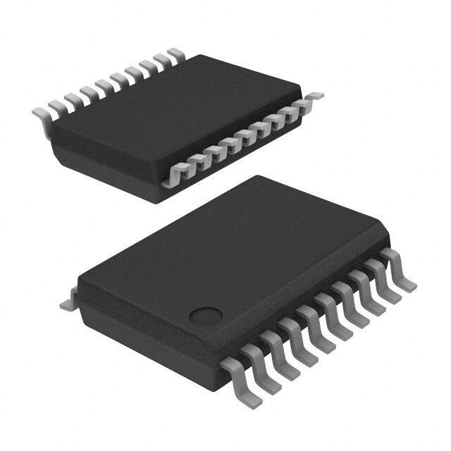
ICGOO电子元器件商城为您提供SP3074EEN-L由Exar设计生产,在icgoo商城现货销售,并且可以通过原厂、代理商等渠道进行代购。 SP3074EEN-L价格参考。ExarSP3074EEN-L封装/规格:接口 - 驱动器,接收器,收发器, 1/1 Transceiver Full RS422, RS485 8-SOIC。您可以下载SP3074EEN-L参考资料、Datasheet数据手册功能说明书,资料中有SP3074EEN-L 详细功能的应用电路图电压和使用方法及教程。
| 参数 | 数值 |
| 产品目录 | 集成电路 (IC)半导体 |
| 描述 | IC TXRX RS485/RS422 ESD 8NSOICRS-422/RS-485 接口 IC RS485/RS422 Driver/ Receiver Transceiver |
| Duplex | Full Duplex |
| 产品分类 | |
| 品牌 | Exar |
| 产品手册 | |
| 产品图片 |
|
| rohs | 符合RoHS无铅 / 符合限制有害物质指令(RoHS)规范要求 |
| 产品系列 | 接口 IC,RS-422/RS-485 接口 IC,Exar SP3074EEN-L- |
| 数据手册 | http://www.exar.com/Common/Content/Document.ashx?id=1399 |
| 产品型号 | SP3074EEN-L |
| PCN其它 | |
| PCN组件/产地 | |
| PCN设计/规格 | |
| 产品种类 | RS-422/RS-485 接口 IC |
| 传播延迟时间ns | 800 ns, 200 ns |
| 供应商器件封装 | 8-SOIC N |
| 关闭 | Yes |
| 其它名称 | 1016-1047-5 |
| 功能 | Transceiver |
| 包装 | 管件 |
| 协议 | RS422,RS485 |
| 双工 | Full Duplex |
| 商标 | Exar |
| 安装类型 | 表面贴装 |
| 安装风格 | SMD/SMT |
| 封装 | Tube |
| 封装/外壳 | 8-SOIC(0.154",3.90mm 宽) |
| 封装/箱体 | SOIC-8 Narrow |
| 工作温度 | -40°C ~ 85°C |
| 工作温度范围 | - 40 C to + 85 C |
| 工作电源电压 | 3.3 V |
| 工厂包装数量 | 98 |
| 接收器滞后 | 100mV |
| 接收机数量 | 1 Receiver |
| 数据速率 | 500 kb/s |
| 最大功率耗散 | 471 mW |
| 最大工作温度 | + 85 C |
| 最小工作温度 | - 40 C |
| 标准包装 | 98 |
| 激励器数量 | 1 Driver |
| 电压-电源 | 3.3V |
| 电源电流 | 1.5 mA |
| 类型 | 收发器 |
| 驱动器/接收器数 | 1/1 |


PDF Datasheet 数据手册内容提取
SP3070E - SP3078E Family Data Sheet ±15kV ESD-Protected, 3.3V, 1/8 Load, Failsafe RS-485/RS-422 Transceivers General Description Features The SP3070E - SP3078E differential line transceivers are ■ ±15kV ESD protection for RS-485 pins suitable for bidirectional communication on balanced ■ 3.3V low-power operation multi-point bus transmission lines and comply with both RS-485 and RS-422 EIA Standards. Each device consists ■ Advanced receiver-failsafe protection for open, shorted of a differential driver and differential receiver. All devices or terminated lines operate from a 3.3V power supply. ■ Up to 256 transceivers may share Bus High receiver input impedance allows a large number of ■ Very low load for 8x greater fanout transceivers to share a common data bus while maintaining signal margin and without excessive loading ■ Hot Swap glitch protection RE and DE or use of expensive repeaters. The high impedance driver ■ Thermal shutdown protects against driver contention output is maintained over the entire common-mode ■ voltage range from -7 to +12V. Receivers will failsafe to Available in three industry standard footprints logic 1 output when inputs are open, shorted or SP3070E, SP3073E and SP3076E in Full-Duplex terminated. Drivers include built-in short-circuit protection (14-pin) and a thermal-overload shutdown to protect against SP3071E, SP3074E and SP3077E in Full-Duplex excessive power dissipation from bus contention or cable (8-pin) faults. All RS-485 receiver inputs and driver outputs are SP3072E, SP3075E and SP3078E in Half-Duplex ESD protected up to ±15kV (Air-Gap and Human Body (8-pin) Model) and up to ±8kV Contact Discharge (IEC 61000-4- ■ Three applications-optimized speed grades 2). The SP3070E - SP3078E devices may not achieve optimal transmit performance if the connected receiver SP3070E - SP3072E: 250kbps slew-limited includes a biasing network to 5.0V without a termination SP3073E - SP3075E: 500kbps slew-limited resistor. Please see MaxLinear Application Note ANI#21 SP3076E - SP3078E: 16Mbps high speed for further details. ■ Small form factor NSOIC packages ■ Industrial (-40 to 85°C) and Extended (-40 to 125°C) Applications temperature grades Industrial Control, Utility Meters, Building Automation, Ordering Information - page19 Instrumentation, Point of Sale NC 1 14 Vcc 8 PIN NSOIC 8 PIN NSOIC RO 2 14 PIN NSOIC 13 NC RO 1 8 Vcc Vcc 1 8 A SP3072E SP3071E RE 3 12 A RE 2 7 B RO 2 7 B SP3070E SP3075E SP3074E DE 4 SP3073E 11 B DE 3 SP3078E 6 A DI 3 SP3077E 6 Z DI 5 SP3076E 10 Z DI 4 Half Duplex 5 GND GND 4 Full Duplex 5 Y GND 6 9 Y Full Duplex GND 7 8 NC Figure 1: Pinouts • www.maxlinear.com• Rev 1.0.3
SP3070E - SP3078E Family RS-485/RS-422 Transceivers Data Sheet Revision History Revision History Document No. Release Date Change Description - Legacy Sipex Datasheet. Convert to Exar format, update ordering information, correct subscript on pages 5-7 and 1.0.0 06/10/09 change revision to 1.0.0. Correct type error on page 7 on driver switching characteristics table. Change 1.0.1 09/30/10 SP3076E,3077E and 3078E Receiver enable time from shutdown from 1800ns to 3000ns. Add reference to Application Note ANI#21 and change ESD protection levels to 1.0.2 12/02/10 IEC 61000-4-2. Update to MaxLinear format, update Ordering Information. Move ESD Protection to page 2. 1.0.3 2/24/20 Corrected 14-pin block diagram (pin 3). 2/24/20 Rev 1.0.3 ii
SP3070E - SP3078E Family ±15kV ESD-Protected, 3.3V, 1/8 Load, Failsafe Data Sheet Table of Contents Table of Contents General Description.............................................................................................................................................i Features............................................................................................................................................................... i Applications.........................................................................................................................................................i Device Architecture and Block Diagrams ........................................................................................................1 14-pin Full Duplex........................................................................................................................................................ 1 8-pin Full Duplex.......................................................................................................................................................... 1 8-pin Half Duplex.......................................................................................................................................................... 1 Specifications.....................................................................................................................................................2 Absolute Maximum Ratings...........................................................................................................................................2 ESD Ratings..................................................................................................................................................................2 Electrical Characteristics...............................................................................................................................................3 Driver Switching Characteristics - SP3070E, SP3071E & SP3072E.............................................................................5 Receiver Switching Characteristics - SP3070E, SP3071E & SP3072E........................................................................5 Driver Switching Characteristics - SP3073E, SP3074E & SP3075E.............................................................................6 Receiver Switching Characteristics - SP3073E, SP3074E & SP3075E........................................................................6 Driver Switching Characteristics - SP3076E, SP3077E & SP3078E.............................................................................7 Receiver Switching Characteristics - SP3076E, SP3077E & SP3078E........................................................................7 Test Circuits and Timing Diagrams...................................................................................................................8 Function Tables................................................................................................................................................12 Pin Information.................................................................................................................................................13 Pin Configurations.......................................................................................................................................................13 Pin Descriptions..........................................................................................................................................................13 Detailed Description.........................................................................................................................................14 Receiver Input Filtering.............................................................................................................................................. 14 Fail Safe..................................................................................................................................................................... 14 Hot-Swap Capability....................................................................................................................................................14 15kV ESD Protection...................................................................................................................................................14 ESD Test Conditions.................................................................................................................................................. 15 IEC 61000-4-2............................................................................................................................................................ 15 Machine Model........................................................................................................................................................... 15 256 Transceivers on the Bus...................................................................................................................................... 15 Reduced EMI and Reflections.................................................................................................................................... 15 Low Power Shutdown Mode....................................................................................................................................... 15 Driver Output Protection............................................................................................................................................. 15 2/24/20 Rev 1.0.3 iii
SP3070E - SP3078E Family ±15kV ESD-Protected, 3.3V, 1/8 Load, Failsafe Data Sheet Table of Contents Line Length................................................................................................................................................................. 15 Typical Applications.................................................................................................................................................... 15 Parts Selector Guide........................................................................................................................................16 Mechanical Dimensions...................................................................................................................................17 NSOIC8.......................................................................................................................................................................17 NSOIC14.....................................................................................................................................................................18 Ordering Information........................................................................................................................................19 2/24/20 Rev 1.0.3 iv
SP3070E - SP3078E Family ±15kV ESD-Protected, 3.3V, 1/8 Load, Failsafe Data Sheet List of Figures List of Figures Figure 1: Pinouts....................................................................................................................................................i Figure 2: 14-pin Full Duplex..................................................................................................................................1 Figure 3: 8-pin Full Duplex....................................................................................................................................1 Figure 4: 8-pin Half Duplex...................................................................................................................................1 Figure 5: Driver DC Test Circuit............................................................................................................................8 Figure 6: Receiver DC Test Circuit.......................................................................................................................8 Figure 7: Driver Propagation Delay Time Test Circuit and Timing Diagram.........................................................8 Figure 8: Driver Enable and Disable Times Test Circuit and Timing Diagram.....................................................9 Figure 9: Driver Contention Test...........................................................................................................................9 Figure 10: Driver Enable and Disable Times Test Circuit and Timing Diagram.................................................10 Figure 11: Receiver Propagation Delay Test Circuit and Timing Diagram.........................................................10 Figure 12: Receiver Enable and Disable Times Test Circuit..............................................................................11 Figure 13: Receiver Enable and Disable Timing Diagram..................................................................................11 Figure 14: Pin Configurations.............................................................................................................................13 Figure 15: Mechanical Dimension, NSOIC8.......................................................................................................17 Figure 16: Mechanical Dimensions, NSOIC14...................................................................................................18 2/24/20 Rev 1.0.3 v
SP3070E - SP3078E Family ±15kV ESD-Protected, 3.3V, 1/8 Load, Failsafe Data Sheet List of Tables List of Tables Table 1: Absolute Maximum Ratings....................................................................................................................2 Table 2: ESD Ratings...........................................................................................................................................2 Table 3: Electrical Characteristics........................................................................................................................3 Table 4: SP3070E, SP3071E & SP3072E Driver Switching Characteristics........................................................5 Table 5: SP3070E, SP3071E & SP3072E Receiver Switching Characteristics...................................................5 Table 6: SP3073E, SP3074E & SP3075E Driver Switching Characteristics........................................................6 Table 7: SP3073E, SP3074E & SP3075E Receiver Switching Characteristics...................................................6 Table 8: SP3076E, SP3077E & SP3078E Driver Switching Characteristics........................................................7 Table 9: SP3076E, SP3077E & SP3078E Receiver Switching Characteristics...................................................7 Table 10: SP3070E, SP3073E, SP3076E (Full Duplex).....................................................................................12 Table 11: SP3070E, SP3073E, SP3076E (Full Duplex).....................................................................................12 Table 12: SP3071E, SP3074E, SP3077E (Full Duplex).....................................................................................12 Table 13: SP3071E, SP3074E, SP3077E (Full Duplex).....................................................................................12 Table 14: SP3072E, SP3075E, SP3078E (Half Duplex)....................................................................................12 Table 15: SP3072E, SP3075E, SP3078E (Half Duplex)....................................................................................12 Table 16: Pin Descriptions..................................................................................................................................13 Table 17: Parts Selector Guide...........................................................................................................................16 Table 18: Ordering Information...........................................................................................................................19 2/24/20 Rev 1.0.3 vi
SP3070E - SP3078E Family RS-485/RS-422 Transceivers Data Sheet Device Architecture and Block Diagrams Device Architecture and Block Diagrams Devices are available in three industry standard architectures and footprints. In each footprint, there are three speed grades available. 1 14 Vcc NC 13 NC 14-pin Full Duplex: 2 12 A R R 11 B 3 SP3070E, 250kbps slew limited RE 4 DE 10 SP3073E, 500kbps slew limited Z 5 D D 6 9 Y SP3076E, 16Mbps GND GND 7 8 NC Figure 2: 14-pin Full Duplex 1 Vcc 8-pin Full Duplex: 2 8 A R R 7 B SP3071E, 250kbps slew limited 6 SP3074E, 500kbps slew limited 3 Z D D 4 5 Y SP3077E, 16Mbps GND Figure 3: 8-pin Full Duplex 8-pin Half Duplex: 8 1 VCC RO R 2 7 SP3072E, 250kbps slew limited RE B DE 3 6 A SP3075E, 500kbps slew limited 4 DI D 5 SP3078E, 16Mbps GND Figure 4: 8-pin Half Duplex 2/24/20 Rev 1.0.3 1
SP3070E - SP3078E Family RS-485/RS-422 Transceivers Data Sheet Specifications Specifications Absolute Maximum Ratings Important: These are stress ratings only and functional operation of the device at these ratings or any other above those indicated in the operation sections of the specifications below is not implied. Exposure to absolute maximum rating conditions for extended periods of time may affect reliability. Table 1: Absolute Maximum Ratings Parameter Minimum Maximum Units VCC 6.0 V Input voltage at control input pins (RE, DE) -0.3 6.0 V Driver input voltage (RE, DE) -0.3 6.0 V Driver output voltage (A, B, Y & Z) -8 13 V Receiver input voltage (A, B) -8 13 V Continuous Power Dissipation at T = 70°C A 8-pin NSOIC (derate 5.88mW/°C above 70°C) 471 mW 14-pin NSOIC (derate 8.33mW/°C above 70°C) 667 mW Operating Temperature Ranges SP307xE_MN -40 125 °C SP307xE_EN -40 85 °C Junction temperature 150 °C Storage temperature range -65 150 °C Lead temperature (soldering, 10s) 300 °C ESD Ratings Table 2: ESD Ratings Parameter Limit Units HBM - Human Body Model (pins Y, Z, A & B) ±15 kV IEC 1000-4-2 Airgap Discharge (pins Y, Z, A & B) ±15 kV IEC 1000-4-2 Contact Discharge (pins Y, Z, A & B) ±8 kV 2/24/20 Rev 1.0.3 2
SP3070E - SP3078E Family RS-485/RS-422 Transceivers Data Sheet Electrical Characteristics Electrical Characteristics Unless otherwise noted, V = 3.3V ±0.3V, ambient temperature T < T < T . Typical values are at V = 3.3V, CC MIN A MAX CC ambient temperature T = 25°C. The "•" denotes the specifications which apply over the full operating range unless A otherwise noted. Table 3: Electrical Characteristics Parameter Symbol Test Condition Minimum Typical Maximum Units RL = 100 (RS-422), Figure 5 2 VCC Differential driver output VOD RL = 54 (RS-485), Figure 5 1.5 VCC V No load • VCC Change in magnitude of differential output voltage VOD RL = 54 or 100, Figure 5 • 0.2 V Driver common mode output voltage VOC RL = 54 or 100, Figure 5 • VCC/2 3 V Change in magnitude of common mode output voltage | VOC | RL = 54 or 100, Figure 5 ±0.2 V Input high voltage VIH DE, DI, RE • 2 V Input low voltage VIL DE, DI, RE 0.8 V Input hysteresis VHYS DE, DI, RE • 100 mV Input current IIN DE, DI, RE • -1 1 µA DE, RE Input impedance first transition First transition will draw more • 1 10 kΩ (hot swap) current (hot swap) Output leakage (Y and Z) DE = GND VIN = 12V • 125 Full duplex (A and B) IO VCC = GND or 3.6V VIN = -7V • -100 µA 0 ±250 Driver short-circuit current IOSD -7V ≤ VOUT ≤ 12V, (Figure 9) mA -250 0 DE = GND VIN = 12V • 125 Input current (A and B) half duplex IA,B VCC = GND or 3.6V VIN = -7V • -100 µA Thermal-shutdown threshold TTS • 165 °C Thermal-shutdown hysteresis TTSH • 15 °C Receiver Receiver differential threshold (sensitivity) VTH -7V ≤ VCM ≤ 12V -200 -125 -50 mV Receiver input hysteresis VTH Va + Vb = 0V • 15 mV RO output high voltage VOH IO = -1mA • VCC - 0.6 V RO output low voltage VOL IO = 1mA • 0.4 V Tri-State output current at receiver IOZR 0 ≤ VO ≤ VCC • ±1 µA Receiver input resistance RIN -7V ≤ VCM ≤ 12V • 96 kΩ Receiver output short-circuit current IOZR 0V ≤ VRO ≤ VCC ±60 mA 2/24/20 Rev 1.0.3 3
SP3070E - SP3078E Family RS-485/RS-422 Transceivers Data Sheet Electrical Characteristics Table 3: Electrical Characteristics Parameter Symbol Test Condition Minimum Typical Maximum Units Supply Current No load, RE = 0, DE = VCC • 0.8 1.5 Supply current ICC No load, RE = VCC, DE = VCC • 0.8 1.5 mA No load, RE = 0, DE = 0 • 0.8 1.5 Supply current in shutdown mode ISHDN RE = VCC, DE = GND 0.05 3 µA 2/24/20 Rev 1.0.3 4
SP3070E - SP3078E Family RS-485/RS-422 Transceivers Data Sheet Switching Characteristics Driver Switching Characteristics - SP3070E, SP3071E & SP3072E Unless otherwise noted, V = 3.3 ±0.3V, ambient temperature T < T < T . Typical values are at V = 3.3V, CC MIN A MAX CC ambient temperature T = 25°C. A Table 4: SP3070E, SP3071E & SP3072E Driver Switching Characteristics Driver Characteristic Conditions Minimum Typical Maximum Unit Data signaling rate Duty cycle 40 to 60% 250 kbps Driver propagation delay (tPHL, tPLH) 250 1500 ns R = 54Ω, C = 50pF, Driver output rise / fall time (tR, tF) L L 350 1600 ns Figure 6 & Figure 7 Driver differential skew (tPLH - tPHL) 200 ns Driver enable to output high (tZH) 2500 ns Driver enable to output low (tZL) RL = 500Ω, CL = 50pF, 2500 ns Driver disable from output high (tHZ) Figure 8 & Figure 10 100 ns Driver disable from output low (tLZ) 100 ns Driver enable from shutdown to output high Figure 8 5500 ns (t ) ZH(SHDN) Driver enable from shutdown to output low Figure 10 5500 ns (t ) ZL(SHDN) Time to shutdown (tSHDN) 50 200 600 ns Receiver Switching Characteristics - SP3070E, SP3071E & SP3072E Unless otherwise noted, V = 3.3 ±0.3V, ambient temperature T < T < T . Typical values are at V = 3.3V, CC MIN A MAX CC ambient temperature T = 25°C. A Table 5: SP3070E, SP3071E & SP3072E Receiver Switching Characteristics Receiver Characteristic Conditions Minimum Typical Maximum Unit Data signaling rate Duty cycle 40 to 60% 250 kbps Receiver propagation delay (tPHL, tPLH) CL = 15pF, Figure 11 & 200 ns Propagation delay skew (tPLH - tPHL) Figure 12 30 ns Receiver enable to output high (tZH) Figure 13 50 ns Receiver enable to output low (tZL) Figure 13 50 ns Receiver disable from output high (tHZ) Figure 13 100 ns Receiver disable from output low (tLZ) Figure 13 200 ns Receiver enable from shutdown to output high Figure 13 4000 ns Receiver enable from shutdown to output low Figure 13 4000 ns Time to shutdown (tSHDN) 50 200 600 ns 2/24/20 Rev 1.0.3 5
SP3070E - SP3078E Family RS-485/RS-422 Transceivers Data Sheet Switching Characteristics Driver Switching Characteristics - SP3073E, SP3074E & SP3075E Unless otherwise noted, V = 3.3 ±0.3V, ambient temperature T < T < T . Typical values are at V = 3.3V, CC MIN A MAX CC ambient temperature T = 25°C. A Table 6: SP3073E, SP3074E & SP3075E Driver Switching Characteristics Driver Characteristic Conditions Minimum Typical Maximum Unit Data signaling rate Duty cycle 40 to 60% 500 kbps Driver propagation delay (tPHL, tPLH) 180 800 ns R = 54Ω, C = 50pF, Driver output rise / fall time (tR, tF) L L 200 800 ns Figure 6 & Figure 7 Driver differential skew (tPLH - tPHL) 100 ns Driver enable to output high (tZH) 2500 ns Driver enable to output low (tZL) RL = 500Ω, CL = 50pF, 2500 ns Driver disable from output high (tHZ) Figure 8 & Figure 10 100 ns Driver disable from output low (tLZ) 100 ns Driver enable from shutdown to output high Figure 8 4500 ns (t ) ZH(SHDN) Driver enable from shutdown to output low Figure 10 4500 ns (t ) ZL(SHDN) Time to shutdown (tSHDN) 50 200 600 ns Receiver Switching Characteristics - SP3073E, SP3074E & SP3075E Unless otherwise noted, V = 3.3 ±0.3V, ambient temperature T < T < T . Typical values are at V = 3.3V, CC MIN A MAX CC ambient temperature T = 25°C. A Table 7: SP3073E, SP3074E & SP3075E Receiver Switching Characteristics Receiver Characteristic Conditions Minimum Typical Maximum Unit Data signaling rate Duty cycle 40 to 60% 500 kbps Receiver propagation delay (tPHL, tPLH) CL = 15pF, Figure 11 & 200 ns Propagation delay skew (tPLH - tPHL) Figure 12 30 ns Receiver enable to output high (tZH) Figure 13 50 ns Receiver enable to output low (tZL) Figure 13 50 ns Receiver disable from output high (tHZ) Figure 13 50 ns Receiver disable from output low (tLZ) Figure 13 50 ns Receiver enable from shutdown to output high Figure 13 4000 ns Receiver enable from shutdown to output low Figure 13 4000 ns Time to shutdown (tSHDN) 50 200 600 ns 2/24/20 Rev 1.0.3 6
SP3070E - SP3078E Family RS-485/RS-422 Transceivers Data Sheet Switching Characteristics Driver Switching Characteristics - SP3076E, SP3077E & SP3078E Unless otherwise noted, V = 3.3 ±0.3V, ambient temperature T < T < T . Typical values are at V = 3.3V, CC MIN A MAX CC ambient temperature T = 25°C. A Table 8: SP3076E, SP3077E & SP3078E Driver Switching Characteristics Driver Characteristic Conditions Minimum Typical Maximum Unit Data signaling rate Duty cycle 40 to 60% 16 Mbps Driver propagation delay (tPHL, tPLH) 50 ns R = 54Ω, C = 50pF, Driver output rise / fall time (tR, tF) L L 15 ns Figure 6 & Figure 8 Driver differential skew (tPLH - tPHL) 8 ns Driver enable to output high (tZH) 150 ns Driver enable to output low (tZL) RL = 500Ω, CL = 50pF, 150 ns Driver disable from output high (tHZ) Figure 8 & Figure 10 100 ns Driver disable from output low (tLZ) 100 ns Driver enable from shutdown to output high Figure 8 1800 ns (t ) ZH(SHDN) Driver enable from shutdown to output low Figure 10 1800 ns (t ) ZL(SHDN) Time to shutdown (tSHDN) 50 200 600 ns Receiver Switching Characteristics - SP3076E, SP3077E & SP3078E Unless otherwise noted, V = 3.3 ±0.3V, ambient temperature T < T < T . Typical values are at V = 3.3V, CC MIN A MAX CC ambient temperature T = 25°C. A Table 9: SP3076E, SP3077E & SP3078E Receiver Switching Characteristics Receiver Characteristic Conditions Minimum Typical Maximum Unit Data signaling rate Duty cycle 40 to 60% 16 Mbps Receiver propagation delay (tPHL, tPLH) CL = 15pF, Figure 11 & 40 75 ns Propagation delay skew (tPLH - tPHL) Figure 12, -40 to 85°C 8 ns Receiver enable to output high (tZH) Figure 13 60 ns Receiver enable to output low (tZL) Figure 13 60 ns Receiver disable from output high (tHZ) Figure 13 50 ns Receiver disable from output low (tLZ) Figure 13 50 ns Receiver enable from shutdown to output high Figure 13 3000 ns Receiver enable from shutdown to output low Figure 13 3000 ns Time to shutdown (tSHDN) 50 200 600 ns 2/24/20 Rev 1.0.3 7
SP3070E - SP3078E Family RS-485/RS-422 Transceivers Data Sheet Test Circuits and Timing Diagrams Test Circuits and Timing Diagrams A R/2 OUT VID B R DI D VOD 0 or 3V R/2 VOC RE VCC Figure 5: Driver DC Test Circuit Figure 6: Receiver DC Test Circuit Y RL CL 54(cid:159) 50pF DI D VOD Z 3.3V V CC V /2 CC DI 0 tPLH t PHL Z V Y O 1/2 V 1/2 V O O V = V(Y) - V(Z) DIFF V V O 10% 90% 90% 10% DIFF -VO tR VSKEW = tPLH - tPHL tF Figure 7: Driver Propagation Delay Time Test Circuit and Timing Diagram 2/24/20 Rev 1.0.3 8
SP3070E - SP3078E Family RS-485/RS-422 Transceivers Data Sheet Test Circuits and Timing Diagrams Y S1 DI 0 or VCC D OUT Z RL = 500(cid:58) CL = 50pF GENERATOR 50(cid:58) V CC V /2 CC DE 0 t t ZL, ZL(SHDN) 0.25V V = (V + V ) / 2 OM OL CC t LZ OUT 0 Figure 8: Driver Enable and Disable Times Test Circuit and Timing Diagram DE = 0 or 3V A/Y IOSD DI = 0 or 3V D B/Z 100(cid:159) -7V to +12V V Figure 9: Driver Contention Test 2/24/20 Rev 1.0.3 9
SP3070E - SP3078E Family RS-485/RS-422 Transceivers Data Sheet Test Circuits and Timing Diagrams VCC Y S1 RL = 500(cid:159) DI 0 or VCC D OUT Z CL = 50pF GENERATOR 50(cid:159) V CC V / 2 CC DE t t 0 ZL, ZL(SHDN) t V OUT LZ CC V = (V + V ) / 2 V OM OL CC 0.25V OL Figure 10: Driver Enable and Disable Times Test Circuit and Timing Diagram A OUT VID B R C L 15pF RE A +1V B -1V t t PHL PLH V OH 1.5V OUT V OL Figure 11: Receiver Propagation Delay Test Circuit and Timing Diagram 2/24/20 Rev 1.0.3 10
SP3070E - SP3078E Family RS-485/RS-422 Transceivers Data Sheet Test Circuits and Timing Diagrams S1 S3 1.5V B 1k(cid:159) VCC -1.5V A R S2 RE CL = 15pF GENERATOR 50(cid:159) Figure 12: Receiver Enable and Disable Times Test Circuit S1 is open S2 is closed S3 = 1.5V S1 is closed, S2 is open, S3 = -1.5V 3V 3V 1.5V 1.5V RE RE 0V t t ZH, ZH(SHDN) t t ZL, ZL(SHDN) V OH V CC OUT V /2 V = V /2 OH OUT OL CC 0V V OL S1 is open S2 is closed S3 = 1.5V S1 is closed, S2 is open, S3 = -1.5V 3V 3V 1.5V 1.5V RE RE t 0V HZ t LZ 0.25V V V OH CC OUT OUT 0V 0.25V V OL Figure 13: Receiver Enable and Disable Timing Diagram 2/24/20 Rev 1.0.3 11
SP3070E - SP3078E Family RS-485/RS-422 Transceivers Data Sheet Function Tables Function Tables Table 10: SP3070E, SP3073E, SP3076E (Full Duplex) Table 11: SP3070E, SP3073E, SP3076E (Full Duplex) Transmitting Receiving Inputs Outputs Inputs Output RE DE DI Z Y RE DE A B RO X 1 1 0 1 0 X -50mV 1 X 1 0 1 0 0 X -200mV 0 0 0 X High-Z Open, X X 1 Shorted 1 0 X Shutdown 1 1 X High-Z 1 0 X Shutdown Table 12: SP3071E, SP3074E, SP3077E (Full Duplex) Table 13: SP3071E, SP3074E, SP3077E (Full Duplex) Transmitting Receiving Input Outputs Inputs Output DI Z Y A, B RO 1 0 1 -50mV 1 0 1 0 -200mV 0 Open / shorted 1 Table 14: SP3072E, SP3075E, SP3078E (Half Duplex) Table 15: SP3072E, SP3075E, SP3078E (Half Duplex) Transmitting Receiving Inputs Outputs Inputs Output RE DE DI B / Z A / Y RE DE A B RO X 1 1 0 1 0 X -50mV 1 X 1 0 1 0 0 X -200mV 0 0 0 X High-Z Open / X X 1 shorted 1 0 X Shutdown 1 1 X High-Z 1 0 X Shutdown 2/24/20 Rev 1.0.3 12
SP3070E - SP3078E Family RS-485/RS-422 Transceivers Data Sheet Pin Information Pin Information Pin Configurations NC 1 14 Vcc 8 PIN NSOIC 8 PIN NSOIC RO 2 14 PIN NSOIC 13 NC RO 1 8 Vcc Vcc 1 8 A SP3072E SP3071E RE 3 12 A RE 2 7 B RO 2 7 B SP3070E SP3075E SP3074E DE 4 SP3073E 11 B DE 3 SP3078E 6 A DI 3 SP3077E 6 Z DI 5 SP3076E 10 Z DI 4 Half Duplex 5 GND GND 4 Full Duplex 5 Y GND 6 9 Y Full Duplex GND 7 8 NC Figure 14: Pin Configurations Pin Descriptions Table 16: Pin Descriptions Pin Number Half Duplex Full Duplex Devices Devices Pin Name Pin Function SP3070E SP3071E SP3072E SP3073E SP3074E SP3075E SP3076E SP3077E SP3078E Receiver Output. When RE is low and if (A-B) ≥ -50mV, RO is 2 2 1 RO High. If (A-B) ≤ -200mV, RO is low. Receiver Output Enable. When RE is low, RO is enabled. When 3 - 2 RE RE is high, RO is high impedance. RE should be high and DE low to enter shutdown mode. RE is a hot swap input. Driver Output Enable. When DE is high, outputs are enabled. 4 - 3 DE When DE is low, outputs are high impedance. DE should be low and RE high to enter shutdown mode. DE is a hot-swap input. Driver Input. With DE high, a low level on DI forces noninverting 5 3 4 DI output low and inverting output high. Similarly, a high level on DI forces noninverting output high and inverting output low. 6, 7 4 5 GND Ground 9 5 - Y Noninverting Driver Output 10 6 - Z Inverting Driver Output 11 7 - B Inverting Receiver Input - - 7 B Inverting Receiver Input and Inverting Driver Output 12 8 - A Noninverting Receiver Input - - 6 A Noninverting Receiver Input and Noninverting Driver Output 14 1 8 VCC Positive Supply VCC. Bypass VCC to GND with a 0.1µF capacitor 1, 8, 13 - - NC No connect. 2/24/20 Rev 1.0.3 13
SP3070E - SP3078E Family RS-485/RS-422 Transceivers Data Sheet Detailed Description Detailed Description The SP307XE family of high speed transceivers for RS-485 Hot-Swap Capability /RS-422 communication contain one driver and one receiver. These devices feature fail-safe circuitry, which When circuit boards are inserted into a hot backplane, guarantees a logic-high receiver output when the receiver differential disturbances to the data bus can lead to data inputs are open or shorted, or when they are connected to errors. Upon initial circuit board insertion, the data a terminated transmission line with all drivers disabled. The communication processor undergoes its own power-up SP3070E, SP3072E, SP3073E, SP3075E, SP3076E and sequence. During this period, the processor's logic-output SP3078E also feature a hot-swap capability allowing live drivers are high impedance and are unable to drive the DE insertion without error data transfer. The SP3070E, and RE inputs of these devices to a defined logic level. SP3071E and SP3072E feature reduced slew-rate drivers Leakage currents up to 10µA from the high-impedance that minimize EMI and reduce reflections caused by state of the processor's logic drivers could cause standard improperly terminated cables, allowing error-free data CMOS enable inputs of a transceiver to drift to an incorrect transmission up to 250kbps. The SP3073E, SP3074E and logic level. Additionally, parasitic circuit board capacitance SP3075E also offer slew-rate limits allowing transmit could cause coupling of V or GND to the enable inputs. speeds up to 500kbps. The SP3076E, SP3077E, CC SP3078E driver slew rates are not limited, making transmit Without the hot-swap capability, these factors could speeds up to 16Mbps possible. improperly enable the transceiver's driver or receiver. When V rises, an internal pulldown circuit holds DE low CC The SP3072E, SP3075E and SP3078E are half-duplex and RE high for approximately 10 microseconds. After the transceivers, while the SP3070E, SP3071E, SP3073E, initial power-up sequence, the pulldown circuit becomes SP3074E, SP3076E and SP3077E are full duplex transparent, resetting the hot-swap tolerable input. transceivers. All devices operate from a single 3.3V supply. Drivers are output short-circuit current limited. Thermal-shutdown 15kV ESD Protection circuitry protects drivers against excessive power dissipation. When activated, the thermal-shutdown circuitry As with all MaxLinear devices, ESD-protection structures places the driver outputs into a high-impedance state. are incorporated on all pins to protect against electrostatic discharges encountered during handling and assembly. The driver output and receiver inputs of the SP3070E Receiver Input Filtering family of devices have extra protection against static electricity. MaxLinear's engineering team have developed SP3070E-SP3075E receivers incorporate input filtering in state of the art structures to protect these pins against ESD addition to input hysteresis. This filtering enhances noise of 15kV without damage. The ESD structures withstand immunity with differential signals that have very slow rise high ESD in all states: normal operation, shutdown and and fall times. Receiver propagation delay increases by powered down. After an ESD event, the SP3070E - 25% due to this filtering. SP3078E keep working without latchup or damage. ESD protection can be tested in various ways. The Fail Safe transmitter outputs and receiver inputs of the SP3070E - SP3078E are characterized for protection to the following The SP3070E family guarantees a logic-high receiver limits: output when the receiver inputs are shorted, open, or when ■ ±15kV using the Human Body Model they are connected to a terminated transmission line with all drivers disabled. If A - B is less than or equal to -200mV, ■ ±8kV using the Contact Discharge method specified in RO is logic low. In the case of a terminated bus with all IEC 61000-4-2 transmitters disabled, the receiver's differential input ■ ±15kV Airgap voltage is pulled to 0V by the termination. With the receiver thresholds of the SP3070E family, this results in a logic high with a 50mV minimum noise margin. In compliance with the EIA / TIA-485 standard, the SP3070E family has a 50mV - 200mV threshold. 2/24/20 Rev 1.0.3 14
SP3070E - SP3078E Family RS-485/RS-422 Transceivers Data Sheet Detailed Description ESD Test Conditions free data transmission up to 250kbps. The SP3073E, SP3074E and SP3075E offer higher driver output slew-rate limits, allowing transmit speeds up to 500kbps. ESD performance depends on a variety of conditions. Contact MaxLinear for a reliability report that documents test setup, methodology and results. Low Power Shutdown Mode IEC 61000-4-2 Low-power shutdown mode is initiated by bringing both RE high and DE low. In shutdown, the devices typically draw The IEC 61000-4-2 standard covers ESD testing and only 50nA of supply current. performance of finished equipment. However, it does not RE and DE can be driven simultaneously; the parts are specifically refer to integrated circuits. The SP3070E family guaranteed not to enter shutdown if RE is high and DE is of devices helps you design equipment to meet IEC 61000- low for less than 50ns. If the inputs are in this state for at 4-2, without the need for additional ESD-protection least 600ns, the parts are guaranteed to enter shutdown. components. Enable times t and t assume the part was not in a low- ZH ZL The major difference between tests done using the Human power shutdown state. Enable times t and ZH(SHDN) Body Model and IEC 61000-4-2 is higher peak current in t assume the parts were shut down. It takes drivers IEC 61000-4-2, because series resistance is lower in the ZL(SHDN) and receivers longer to become enabled from low-power IEC 1000-4-2 model. Hence, the ESD withstand voltage shutdown mode t and t than from driver / measured to IEC 61000-4-2 is generally lower than that ZH(SHDN) ZL(SHDN) measured using the Human Body Model. receiver-disable mode (tZH, tZL). The air-gap test involves approaching the device with a charged probe. The contact-discharge method connects Driver Output Protection the probe to the device before the probe is energized. Two mechanisms prevent excessive output current and Machine Model power dissipation caused by faults or by bus contention. First, current limit on the output stage, provides immediate protection against short circuits over the whole common- The machine model for ESD tests all pins using a 200pF mode voltage range. storage capacitor and zero discharge resistance. The objective is to emulate the stress caused when I/O pins are Second, a thermal-shutdown circuit, forces the driver contacted by handling equipment during test and outputs into a high-impedance state if the die temperature assembly. becomes excessive. 256 Transceivers on the Bus Line Length The standard RS-485 receiver input impedance is 12kΩ The RS-485/RS422 standard covers line lengths up to (1 unit load), and the standard driver can drive up to 32 unit 4000ft. loads. The SP3070E family of transceivers has a 1/8-unit load receiver input impedance (96kΩ), allowing up to 256 Typical Applications transceivers to be connected in parallel on one communication line. Any combination of these devices as well as other RS-485 transceivers with a total of 32 unit The SP3072E, SP3075E and SP3078E transceivers are loads or fewer can be connected to the line. designed for bidirectional data communications on multipoint bus transmission lines. Reduced EMI and Reflections To minimize reflections, terminate the line at both ends in its characteristic impedance, and keep stub lengths off the main line as short as possible. The slew-rate-limited The SP3070E, SP3071E and SP3072E feature reduced SP3070E - SP3075E are more tolerant of imperfect slew-rate drivers that minimize EMI and reduce reflections termination. caused by improperly terminated cables, allowing error- 2/24/20 Rev 1.0.3 15
SP3070E - SP3078E Family RS-485/RS-422 Transceivers Data Sheet Parts Selector Guide Parts Selector Guide Table 17: Parts Selector Guide Receiver Part Half / Full Data Rate Transceivers Pin Industry Standard Pin Compatible Shutdown Driver Number Duplex (Mbps) on Bus Count Pinout Upgrade from: Enable SP3070E Full 0.25 Yes Yes 256 14 MAX3070E, 75180 SP3071E Full 0.25 No No 256 8 MAX3071E, 75179 SP3493 SP3072E Half 0.25 Yes Yes 256 8 MAX3072E, 75176 SP3483 SP3073E Full 0.5 Yes Yes 256 14 MAX3073E, 75180 SP3074E Full 0.5 No No 256 8 MAX3074E, 75179 SP3075E Half 0.5 Yes Yes 256 8 MAX3075E, 75176 SP3494 SP3076E Full 16 Yes Yes 256 14 MAX3076E, 75180 SP3491 SP3077E Full 16 No No 256 8 MAX3077E, 75179 SP3490 SP3078E Half 16 Yes Yes 256 8 MAX3078E, 75176 SP3485, SP3481 2/24/20 Rev 1.0.3 16
SP3070E - SP3078E Family RS-485/RS-422 Transceivers Data Sheet Mechanical Dimensions Mechanical Dimensions NSOIC8 Side View Front View Drawing No: POD-00000108 Revision: A Figure 15: Mechanical Dimension, NSOIC8 2/24/20 Rev 1.0.3 17
SP3070E - SP3078E Family RS-485/RS-422 Transceivers Data Sheet Mechanical Dimensions Mechanical Dimensions NSOIC14 Top View Side View Front View Drawing No:POD-00000109 Revision: A Figure 16: Mechanical Dimensions, NSOIC14 2/24/20 Rev 1.0.3 18
SP3070E - SP3078E Family RS-485/RS-422 Transceivers Data Sheet Ordering Information Ordering Information Table 18: Ordering Information Ordering Part Number Operating Temperature Range Package Packaging Method Lead-Free(2) Duplex / Data Rate SP3070E SP3070EEN-L -40°C to 85°C NSOIC14 Tube Yes Full / 250kbps SP3070EEN-L/TR -40°C to 85°C NSOIC14 Reel Yes Full / 250kbps SP3071E SP3071EEN-L -40°C to 85°C NSOIC8 Tube Yes Full / 250kbps SP3071EEN-L/TR -40°C to 85°C NSOIC8 Reel Yes Full / 250kbps SP3072E SP3072EEN-L -40°C to 85°C NSOIC8 Tube Yes Half / 250kbps SP3072EEN-L/TR -40°C to 85°C NSOIC8 Reel Yes Half / 250kbps SP3072EMN-L/TR -40°C to 125°C NSOIC8 Reel Yes Half / 250kbps SP3073E SP3073EEN-L/TR -40°C to 85°C NSOIC14 Reel Yes Full / 500kbps SP3074E SP3074EEN-L/TR -40°C to 85°C NSOIC8 Reel Yes Full / 500kbps SP3075E SP3075EEN-L -40°C to 85°C NSOIC8 Tube Yes Half / 500kbps SP3075EEN-L/TR -40°C to 85°C NSOIC8 Reel Yes Half / 500kbps SP3076E SP3076EEN-L -40°C to 85°C NSOIC14 Tube Yes Full / 16Mbps SP3076EEN-L/TR -40°C to 85°C NSOIC14 Reel Yes Full / 16Mbps SP3076EMN-L/TR -40°C to 125°C NSOIC14 Reel Yes Full / 16Mbps SP3077E SP3077EEN-L -40°C to 85°C NSOIC8 Tube Yes Full / 16Mbps SP3077EEN-L/TR -40°C to 85°C NSOIC8 Reel Yes Full / 16Mbps SP3078E SP3078EEN-L -40°C to 85°C NSOIC8 Tube Yes Half / 16Mbps SP3078EEN-L/TR -40°C to 85°C NSOIC8 Reel Yes Half / 16Mbps SP3078EMN-L/TR -40°C to 125°C NSOIC8 Reel Yes Half / 16Mbps 1.Refer to http://www.maxlinear.com/SP3070E, http://www.maxlinear.com/SP3071E, http://www.maxlinear.com/SP3072E, http://www.maxlinear.com/ SP3073E, http://www.maxlinear.com/SP3074E, http://www.maxlinear.com/SP3075E, http://www.maxlinear.com/SP3076E, http://www.maxlinear.com/ SP3077E and http://www.maxlinear.com/SP3078E for most up-to-date Ordering Information. 2.Visit www.maxlinear.com for additional information on Environmental Rating. 2/24/20 Rev 1.0.3 19
SP3070E - SP3078E Family RS-485/RS-422 Transceivers Data Sheet Disclaimer MaxLinear, Inc. 5966 La Place Court, Suite 100 Carlsbad, CA 92008 760.692.0711 p. 760.444.8598 f. www.maxlinear.com The content of this document is furnished for informational use only, is subject to change without notice, and should not be construed as a commitment by MaxLinear, Inc. MaxLinear, Inc. assumes no responsibility or liability for any errors or inaccuracies that may appear in the informational content contained in this guide. Complying with all applicable copyright laws is the responsibility of the user. Without limiting the rights under copyright, no part of this document may be reproduced into, stored in, or introduced into a retrieval system, or transmitted in any form or by any means (electronic, mechanical, photocopying, recording, or otherwise), or for any purpose, without the express written permission of MaxLinear, Inc. Maxlinear, Inc. does not recommend the use of any of its products in life support applications where the failure or malfunction of the product can reasonably be expected to cause failure of the life support system or to significantly affect its safety or effectiveness. Products are not authorized for use in such applications unless MaxLinear, Inc. receives, in writing, assurances to its satisfaction that: (a) the risk of injury or damage has been minimized; (b) the user assumes all such risks; (c) potential liability of MaxLinear, Inc. is adequately protected under the circumstances. MaxLinear, Inc. may have patents, patent applications, trademarks, copyrights, or other intellectual property rights covering subject matter in this document. Except as expressly provided in any written license agreement from MaxLinear, Inc., the furnishing of this document does not give you any license to these patents, trademarks, copyrights, or other intellectual property. MaxLinear, the MaxLinear logo, and any MaxLinear trademarks, MxL, Full-Spectrum Capture, FSC, G.now, AirPHY and the MaxLinear logo are all on the products sold, are all trademarks of MaxLinear, Inc. or one of MaxLinear’s subsidiaries in the U.S.A. and other countries. All rights reserved. Other company trademarks and product names appearing herein are the property of their respective owners. © 2009-2020 MaxLinear, Inc. All rights reserved.