ICGOO在线商城 > 集成电路(IC) > PMIC - 配电开关,负载驱动器 > SP2525A-1EN-L

 Datasheet下载
- 型号: SP2525A-1EN-L
- 制造商: Exar
- 库位|库存: xxxx|xxxx
- 要求:
| 数量阶梯 | 香港交货 | 国内含税 |
| +xxxx | $xxxx | ¥xxxx |
查看当月历史价格
查看今年历史价格
SP2525A-1EN-L产品简介:
ICGOO电子元器件商城为您提供SP2525A-1EN-L由Exar设计生产,在icgoo商城现货销售,并且可以通过原厂、代理商等渠道进行代购。 SP2525A-1EN-L价格参考。ExarSP2525A-1EN-L封装/规格:PMIC - 配电开关,负载驱动器, 。您可以下载SP2525A-1EN-L参考资料、Datasheet数据手册功能说明书,资料中有SP2525A-1EN-L 详细功能的应用电路图电压和使用方法及教程。
| 参数 | 数值 |
| 产品目录 | 集成电路 (IC)半导体 |
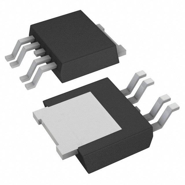
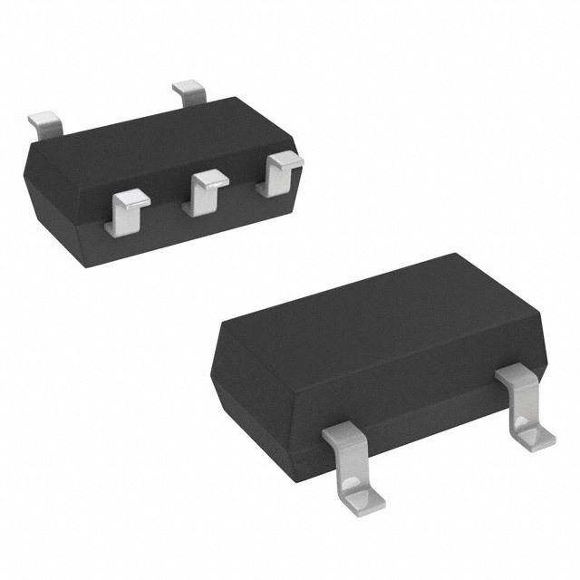
| 描述 | IC USB PWR SW HIGH-SIDE 8NSOICUSB开关IC 1-CH Active High temp -40C to 85C |
| 产品分类 | PMIC - MOSFET,电桥驱动器 - 内部开关集成电路 - IC |
| 品牌 | Exar Corporation |
| 产品手册 | |
| 产品图片 |
|
| rohs | 符合RoHS无铅 / 符合限制有害物质指令(RoHS)规范要求 |
| 产品系列 | 开关 IC,USB开关IC,Exar SP2525A-1EN-L- |
| 数据手册 | http://www.exar.com/Common/Content/Document.ashx?id=627 |
| 产品型号 | SP2525A-1EN-L |
| Rds(On) | 70 毫欧 |
| 产品种类 | USB开关IC |
| 供应商器件封装 | 8-SOIC N |
| 其它名称 | 1016-1036-5 |
| 包装 | 管件 |
| 商标 | Exar |
| 安装类型 | 表面贴装 |
| 安装风格 | SMD/SMT |
| 导通电阻 | 70 毫欧 |
| 封装 | Tube |
| 封装/外壳 | 8-SOIC(0.154",3.90mm 宽) |
| 封装/箱体 | SOIC-8 Narrow |
| 工作温度 | -40°C ~ 85°C |
| 工厂包装数量 | 98 |
| 开关数量 | Dual |
| 开关类型 | USB 开关 |
| 接口 | 开/关 |
| 最大工作温度 | + 85 C |
| 最小工作温度 | - 40 C |
| 标准包装 | 98 |
| 比率-输入:输出 | 1:1 |
| 特性 | 状态标志 |
| 电压-电源 | 3 V ~ 5.5 V |
| 电压-电源(Vcc/Vdd) | 不需要 |
| 电压-负载 | 3 V ~ 5.5 V |
| 电流-峰值输出 | 1A |
| 电流-输出/通道 | 500mA |
| 电流-输出(最大值) | 500mA |
| 电源电压-最大 | 5.5 V |
| 电源电压-最小 | 3 V |
| 类型 | 高端开关 |
| 输入类型 | 非反相 |
| 输出数 | 1 |
| 输出类型 | N 通道 |
| 输出配置 | 高端 |


- 商务部:美国ITC正式对集成电路等产品启动337调查
- 曝三星4nm工艺存在良率问题 高通将骁龙8 Gen1或转产台积电
- 太阳诱电将投资9.5亿元在常州建新厂生产MLCC 预计2023年完工
- 英特尔发布欧洲新工厂建设计划 深化IDM 2.0 战略
- 台积电先进制程称霸业界 有大客户加持明年业绩稳了
- 达到5530亿美元!SIA预计今年全球半导体销售额将创下新高
- 英特尔拟将自动驾驶子公司Mobileye上市 估值或超500亿美元
- 三星加码芯片和SET,合并消费电子和移动部门,撤换高东真等 CEO
- 三星电子宣布重大人事变动 还合并消费电子和移动部门
- 海关总署:前11个月进口集成电路产品价值2.52万亿元 增长14.8%


PDF Datasheet 数据手册内容提取
SSPP22552255AA SSiinnggllee CChhaannnneell UUSSBB PPoowweerr DDiissttrriibbuuttiioonn SSwwiittcchh November 2011 Rev. 2.1.0 GENERAL DESCRIPTION APPLICATIONS The SP2525A device is an integrated high-side Self Powered USB 2.0 and 3.0 Hubs power switch ideal for self-powered and bus- USB Compliant V Power Distribution powered Universal Serial Bus (USB) BUS applications. Audio-Video Equipments The high-side switches are MOSFETs with Generic Power Switching 70mΩ R , which meets USB voltage drop DS(ON) requirements for maximum transmission wire FEATURES length. Multi-purpose open-drain fault flag output indicates over-current limiting, thermal +3.0V to +5.5V Input Voltage Range shutdown, or under voltage lockout. Output 500mA Continuous Load Current current is typically limited to 0.85A below the per Channel 5A safety requirement, and the thermal shutdown function shuts the switch off to 2.6V Undervoltage Lockout prevent damage under overcurrent conditions. 1.25A Short Circuit Current Limit Guaranteed minimum output rise time limits inrush current during hot plug-in, minimizing 100mΩ Maximum On-Resistance EMI and preventing the voltage at the 75μA On-State Supply Current upstream port from dropping excessively. 1μA Shutdown Current The SP2525A is offered in a RoHS compliant “green”/halogen free 8-pin NSOIC package. Output can be Forced Higher than Input (Off-State) Thermal Shutdown Slow Turn On and Fast Turn Off Active-high Version: SP2525A-1 Active-low Version: SP2525A-2 RoHS Compliant, Green/Halogen Free 8-Pin NSOIC Package TYPICAL APPLICATION DIAGRAM Fig. 1: SP2525A Application Diagram – Single Port Self Powered Hub Exar Corporation www.exar.com 48720 Kato Road, Fremont CA 94538, USA Tel. +1 510 668-7000 – Fax. +1 510 668-7001
SSPP22552255AA SSiinnggllee CChhaannnneell UUSSBB PPoowweerr DDiissttrriibbuuttiioonn SSwwiittcchh ABSOLUTE MAXIMUM RATINGS OPERATING RATINGS These are stress ratings only and functional operation of Ambient Temperature Range ..................... -40°C to 85°C the device at these ratings or any other above those indicated in the operation sections of the specifications below is not implied. Exposure to absolute maximum rating conditions for extended periods of time may affect reliability. Supply Voltage V ................................................. 7.0V IN Fault Flag Voltage V ............................................ 7.0V FLG Fault Flag Current I ........................................... 50mA FLG Enable Input V ......................................... -0.3V to 15V EN Storage Temperature .............................. -65°C to 150°C Power Dissipation (NSOIC-8) ......................................... (derate 6.14mW/°C above 70°C) ...................... 500mW ELECTRICAL SPECIFICATIONS Specifications with standard type are for an Operating Ambient Temperature of T = 25°C only; limits applying over the full A Operating Junction Temperature range are denoted by a “•”. Minimum and Maximum limits are guaranteed through test, design, or statistical correlation. Typical values represent the most likely parametric norm at T = 25°C, and are provided A for reference purposes only. Unless otherwise indicated, V = 5.0V, T = 25°C. IN A Parameter Min. Typ. Max. Units Conditions Supply Current 0.75 5.0 µA VEN = Logic “0” OUT =open 75 100 VEN = Logic “1” OUT =open Enable Input Voltage 0.8 1.7 V VEN = Logic “0” 2.0 2.4 VEN = Logic “1” Enable Input Current 0.01 1 µA VEN = Logic “0” 0.01 1 VEN = Logic “1” Enable Input Capacitance 1 pF Output MOSFET Resistance 70 100 mΩ Output turn-on delay 100 µs RL=10Ω, each output Output turn-on rise time 1000 4000 µs RL=10Ω, each output Output turn-off delay 0.8 20 µs RL=10Ω, each output Output turn-off fall time 0.7 20 µs RL=10Ω, each output Output Leakage Current 10 µA Current limit threshold 0.6 1.0 1.25 A Over temperature shutdown 135 °C Temperature TJ raising threshold 125 Temperature TJ decreasing Error Flag Output Resistance 10 25 Ω VIN=5V, IL=10mA 15 40 VIN=3.3V, IL=10mA Error Flag Current 0.01 1 µA UVLO threshold 2.6 V VIN increasing 2.4 VIN decreasing © 2011 Exar Corporation 2/10 Rev. 2.1.0
SSPP22552255AA SSiinnggllee CChhaannnneell UUSSBB PPoowweerr DDiissttrriibbuuttiioonn SSwwiittcchh BLOCK DIAGRAM Fig. 2: SP2525A Block Diagram PIN ASSIGNMENT Fig. 3: SP2525A Pin Assignment PIN DESCRIPTION Name Pin Number Description EN 1 Enable Input Active High for SP2525A-1 and Active Low for SP2525A-2 An active-low and open-drained fault flag output for power switch. It can indicate FLG 2 current limit if CTL is active. In normal mode operation, it also can indicate thermal shutdown or under voltage GND 3 Chip Power Ground NC 4 Not Internally Connected IN 5, 7 Power Supply Input OUT 6, 8 MOSFET Switch Output © 2011 Exar Corporation 3/10 Rev. 2.1.0
SSPP22552255AA SSiinnggllee CChhaannnneell UUSSBB PPoowweerr DDiissttrriibbuuttiioonn SSwwiittcchh ORDERING INFORMATION Temperature Packing Part Number Marking Package Note 1 Note 2 Range Quantity SP2525A-1EN-L -40°C≤TA≤+85°C Sipex Bulk RoHS Compliant Enable 2525A-1E NSOIC8 SP2525A-1EN-L/TR -40°C≤T ≤+85°C 2.5K/Tape & Reel Halogen Free Active high A YYWWL SP2525A-2EN-L -40°C≤TA≤+85°C Sipex Bulk RoHS Compliant Enable Active 2525A-2E NSOIC8 SP2525A-2EN-L/TR -40°C≤T ≤+85°C 2.5K/Tape & Reel Halogen Free Low A YYWWL “YY” = Year – “WW” = Work Week – “X” = Lot Number © 2011 Exar Corporation 4/10 Rev. 2.1.0
SSPP22552255AA SSiinnggllee CChhaannnneell UUSSBB PPoowweerr DDiissttrriibbuuttiioonn SSwwiittcchh TYPICAL PERFORMANCE CHARACTERISTICS All data taken at V = 5.0V, T = 25°C, unless otherwise specified - Schematic and BOM from Application Information IN A section of this datasheet. Fig. 4: Output On-Resistance vs Supply Voltage Fig. 5: Output On-Resistance vs Temperature Fig. 6: UVLO Threshold vs Temperature Fig. 7: On-state Supply Current vs Supply Voltage Fig. 8: On-state Supply Current vs Temperature Fig. 9: Off-state Supply Current vs Supply Voltage © 2011 Exar Corporation 5/10 Rev. 2.1.0
SSPP22552255AA SSiinnggllee CChhaannnneell UUSSBB PPoowweerr DDiissttrriibbuuttiioonn SSwwiittcchh Fig. 10: CTL Threshold vs Supply Voltage Fig. 11: Current Limit Threshold vs Temperature Fig. 12: Output Rise Time vs Temperature Fig. 13: Output Fall Time vs Temperature Fig. 14: Input Voltage Response Fig. 15: Turn-On, Turn-Off Characteristics © 2011 Exar Corporation 6/10 Rev. 2.1.0
SSPP22552255AA SSiinnggllee CChhaannnneell UUSSBB PPoowweerr DDiissttrriibbuuttiioonn SSwwiittcchh Fig. 16: Turn-On, Turn-Off Characteristics Fig. 17: Turn-On, Turn-Off Characteristics Fig. 18: Short Circuit Response Fig. 19: Short Circuit Response (Short applied to Output) (Enable to Short Circuit) Fig. 20: Short Circuit Transient Response Fig. 21: Current Limit Response (Short applied to Output) (Ramped Load) © 2011 Exar Corporation 7/10 Rev. 2.1.0
SSPP22552255AA SSiinnggllee CChhaannnneell UUSSBB PPoowweerr DDiissttrriibbuuttiioonn SSwwiittcchh APPLICATION INFORMATION SHORT CIRCUIT TRANSIENT Bulk capacitance provides the short-term ERROR FLAG transient current needed during a hot- The Error Flag is an open-drained output of an attachment event. A 33μF/16V tantalum or a N-channel MOSFET, the FLG output is pulled 100μF/ 10V electrolytic capacitor mounted low to signal the following fault conditions: close to the downstream connector at each input undervoltage, output current limit, and port should provide sufficient transient drop thermal shutdown. protection. CURRENT LIMIT PRINTED CIRCUIT LAYOUT The current limit threshold is preset internally. The Power circuitry of USB printed circuit It protects the output MOSFET switches from boards requires a customized layout to damage resulting from undesirable short maximize thermal dissipation and to minimize circuit conditions or excess inrush current, voltage drop and EMI. which is often encountered during hot plug-in. The low limit of the current limit threshold of INPUT AND OUTPUT the SP2525A allows a minimum current of The independent solid state switch connects 0.5A through the MOSFET switches. A current the IN pin to the OUT pin when enabled by a limit condition will signal the Error Flag. logic signal at EN. The IN pin is the power supply connection to the internal circuitry and THERMAL SHUTDOWN the drain of the output MOSFET. The OUT pin When the temperature of the SP2525A is the source for the MOSFET. Typically, the exceeds 135ºC for any reasons, the thermal current in USB application will flow through shutdown function turns off the MOSFET the switch from IN to OUT towards the load. If switch and signals the Error Flag. A hysteresis VOUT is greater than VIN when a switch is of 10ºC prevents the MOSFETs from turning enabled, the current will flow from OUT to the back on until the chip temperature drops IN pin because the MOSFET channels are below 125ºC. bidirectional when switched on. The output source is allowed to be externally forced to a SUPPLY FILTERING higher voltage than its input without causing unwanted current flow when the output is A 0.1μF to 1μF bypass capacitor from IN to disabled. GND, located near the device, is strongly recommended to control supply transients. Without a bypass capacitor, an output short TEST CIRCUIT may cause ringing on the input (from supply lead inductance) which can damage internal control circuitry. TRANSIENT REQUIREMENTS USB supports dynamic attachment (hot plugin) of peripherals. A current surge is caused by the input capacitance of a downstream device. Ferrite beads are recommended in series with all power and ground connector pins. Ferrite beads reduce EMI and limit the inrush current during hot- attachment by filtering high-frequency signals. © 2011 Exar Corporation 8/10 Rev. 2.1.0
SSPP22552255AA SSiinnggllee CChhaannnneell UUSSBB PPoowweerr DDiissttrriibbuuttiioonn SSwwiittcchh PACKAGE SPECIFICATION 8-PIN NSOIC © 2011 Exar Corporation 9/10 Rev. 2.1.0
SSPP22552255AA SSiinnggllee CChhaannnneell UUSSBB PPoowweerr DDiissttrriibbuuttiioonn SSwwiittcchh REVISION HISTORY Revision Date Description 2.0.0 11/10/2010 Reformat of datasheet 2.1.1 11/04/2011 Updated package specification FOR FURTHER ASSISTANCE Email: customersupport@exar.com Exar Technical Documentation: http://www.exar.com/TechDoc/default.aspx? EXAR CORPORATION HEADQUARTERS AND SALES OFFICES 48720 Kato Road Fremont, CA 94538 – USA Tel.: +1 (510) 668-7000 Fax: +1 (510) 668-7030 www.exar.com NOTICE EXAR Corporation reserves the right to make changes to the products contained in this publication in order to improve design, performance or reliability. EXAR Corporation assumes no responsibility for the use of any circuits described herein, conveys no license under any patent or other right, and makes no representation that the circuits are free of patent infringement. Charts and schedules contained here in are only for illustration purposes and may vary depending upon a user’s specific application. While the information in this publication has been carefully checked; no responsibility, however, is assumed for inaccuracies. EXAR Corporation does not recommend the use of any of its products in life support applications where the failure or malfunction of the product can reasonably be expected to cause failure of the life support system or to significantly affect its safety or effectiveness. Products are not authorized for use in such applications unless EXAR Corporation receives, in writing, assurances to its satisfaction that: (a) the risk of injury or damage has been minimized; (b) the user assumes all such risks; (c) potential liability of EXAR Corporation is adequately protected under the circumstances. Reproduction, in part or whole, without the prior written consent of EXAR Corporation is prohibited. © 2011 Exar Corporation 10/10 Rev. 2.1.0