 Datasheet下载
- 型号: SP1011-04UTG
- 制造商: Littelfuse
- 库位|库存: xxxx|xxxx
- 要求:
| 数量阶梯 | 香港交货 | 国内含税 |
| +xxxx | $xxxx | ¥xxxx |
查看当月历史价格
查看今年历史价格
SP1011-04UTG产品简介:
ICGOO电子元器件商城为您提供SP1011-04UTG由Littelfuse设计生产,在icgoo商城现货销售,并且可以通过原厂、代理商等渠道进行代购。 SP1011-04UTG价格参考。LittelfuseSP1011-04UTG封装/规格:TVS - 二极管, 。您可以下载SP1011-04UTG参考资料、Datasheet数据手册功能说明书,资料中有SP1011-04UTG 详细功能的应用电路图电压和使用方法及教程。
| 参数 | 数值 |
| 产品目录 | |
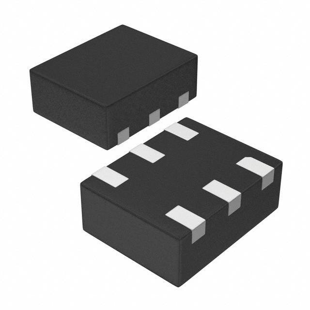
| 描述 | TVS DIODE 6VWM 10.2VC UDFN6TVS二极管阵列 4 Ch 15kV 5V TVS Diode Array |
| 产品分类 | |
| 品牌 | Littelfuse Inc |
| 产品手册 | |
| 产品图片 |
|
| rohs | 符合RoHS无铅 / 符合限制有害物质指令(RoHS)规范要求 |
| 产品系列 | 二极管与整流器,TVS二极管,TVS二极管阵列,Littelfuse SP1011-04UTGSP1011, SPA® |
| 数据手册 | |
| 产品型号 | SP1011-04UTG |
| 不同频率时的电容 | - |
| 产品培训模块 | http://www.digikey.cn/PTM/IndividualPTM.page?site=cn&lang=zhs&ptm=22970http://www.digikey.cn/PTM/IndividualPTM.page?site=cn&lang=zhs&ptm=25590 |
| 产品目录绘图 |
|
| 产品目录页面 | |
| 产品种类 | TVS二极管阵列 |
| 供应商器件封装 | 6-µDFN (1.25x1.0) |
| 其它名称 | F3504TR |
| 击穿电压 | 6 V |
| 功率-峰值脉冲 | - |
| 包装 | 带卷 (TR) |
| 单向通道 | 4 |
| 双向通道 | - |
| 商标 | Littelfuse |
| 商标名 | SPA |
| 安装类型 | 表面贴装 |
| 安装风格 | SMD/SMT |
| 封装 | Reel |
| 封装/外壳 | 6-XDFN |
| 封装/箱体 | uDFN-6 |
| 尺寸 | 1.05 mm W x 1.3 mm L x 0.55 mm H |
| 峰值浪涌电流 | 2 A |
| 工作温度 | -40°C ~ 125°C (TJ) |
| 工作电压 | 6 V |
| 工厂包装数量 | 3000 |
| 应用 | 通用 |
| 最大工作温度 | + 85 C |
| 最小工作温度 | - 40 C |
| 极性 | Unidirectional |
| 标准包装 | 3,000 |
| 特色产品 | http://www.digikey.com/cn/zh/ph/Littelfuse/SP1000.html |
| 电压-击穿(最小值) | 7V |
| 电压-反向关态(典型值) | 6V (最小值) |
| 电压-箝位(最大值)@Ipp | 10.2V |
| 电容 | 7 pF |
| 电流-峰值脉冲(10/1000µs) | 2A (8/20µs) |
| 电源线路保护 | 无 |
| 端接类型 | SMD/SMT |
| 类型 | 齐纳 |
| 系列 | SP1011 |
| 通道 | 4 Channels |
| 钳位电压 | 7.8 V |


PDF Datasheet 数据手册内容提取
TVS Diode Arrays (SPA® Diodes) General Purpose ESD Protection - SP1011 Series SP1011 Series 7pF 15kV Unidirectional TVS Array RoHS Pb GREEN Description Zener diodes fabricated in a proprietary silicon avalanche technology protect each I/O pin to provide a high level of protection for electronic equipment that may experience destructive electrostatic discharges (ESD). These robust diodes can safely absorb repetitive ESD strikes above the maximum level specified in the IEC 61000-4-2 international standard (Level 4, ±8kV contact discharge) without performance degradation. Their very low loading capacitance also makes them ideal for protection high- speed signal pins. Pinout Features • RoHS compliant and • Low leakage current of I/O (1) I/O (4) lead-free 1µA (MAX) at 5V • ESD, IEC 61000-4-2, • Tiny μDFN( JEDEC MO- GND GND ±15kV contact, ±30kV air 229) package (1.25mm x I/O (2) I/O (3) • Lightning, IEC 61000- 1.0mm x 0.5mm) 4-5, 2nd Edition, 2A • EFT protection µDFN-6 (t =8/20µs) IEC 61000-4-4, 40A p (1.25x1.0x0.5mm) • Low capacitance of 7 pF (5/50ns) (TYP) per I/O @ 2.5V Functional Block Diagram Applications 6 5 4 • LCD/PDP TV • Mobile Phone • DVD Player • Notebook • Desktop • MP3/PMP • Set Top Box • Digital camera Application Example 1 2 3 Keyboard Input Additional Information Controller D1 D2 O D3 u D4 ts Resources Samples id e W o r SP1011-04UTG ld Signal Ground Shield Ground Life Support Note: Not Intended for Use in Life Support or Life Saving Applications The products shown herein are not designed for use in life sustaining or life saving applications unless otherwise expressly indicated. © 2017 Littelfuse, Inc. Specifications are subject to change without notice. Revised: 05/12/17
TVS Diode Arrays (SPA® Diodes) General Purpose ESD Protection - SP1011 Series Absolute Maximum Ratings Symbol Parameter Value Units I Peak Pulse Current (t=8/20μs) 2 A PP p T Operating Temperature –40 to 125 °C OP T Storage Temperature –55 to 150 °C STOR CAUTION: Stresses above those listed in “Absolute Maximum Ratings” may cause permanent damage to the device. This is a stress only rating and operation of the device at these or any other conditions above those indicated in the operational sections of this specification is not implied. Thermal Information Parameter Rating Units Storage Temperature Range –55 to 150 °C Maximum Junction Temperature 150 °C Maximum Lead Temperature (Soldering 20-40s) 260 °C Electrical Characteristics (T =25ºC) OP Parameter Symbol Test Conditions Min Typ Max Units Reverse Voltage Drop V I = 1mA 6.0 8.5 V R R Reverse Standoff Voltage V I ≤1µA 6 V RWM R Reverse Leakage Current I V = 5V 0.1 1 µA LEAK R I =1A, t=8/20μs, Fwd 8.7 V PP p Clamp Voltage1 V C I =2A, t=8/20μs, Fwd 10.2 V PP p Dynamic Resistance R (V - V ) / (I - I ) 1.5 Ω DYN C2 C1 PP2 PP1 IEC 61000-4-2 (Contact Discharge) ±15 kV ESD Withstand Voltage1 V ESD IEC 61000-4-2 (Air Discharge) ±30 kV Reverse Bias = 0V 12 15 pF Diode Capacitance1 C D Reverse Bias = 2.5V 7 pF Note: 1. Parameter is guaranteed by design and/or device characterization. Capacitance vs. Reverse Bias Insertion Loss (S21) I/O to GND 14.0 5 12.0 0 nce (pF) 180..00 on (dB)-1-05 acita 6.0 nuati-15 Cap 4.0 Atte-20 2.0 -25 0.0 -30 0.0 0.5 1.0 1.5 2.0 2.5 3.0 3.5 4.0 4.5 5.0 10 100 1000 10000 DC Bias (V) Frequency (MHz) © 2017 Littelfuse, Inc. Specifications are subject to change without notice. Revised: 05/12/17
TVS Diode Arrays (SPA® Diodes) General Purpose ESD Protection - SP1011 Series Soldering Parameters Reflow Condition Pb – Free assembly - Temperature Min (T ) 150°C s(min) Pre Heat - Temperature Max (T ) 200°C s(max) - Time (min to max) (t) 60 – 180 secs s Average ramp up rate (Liquidus) Temp 3°C/second max (T) to peak L T to T - Ramp-up Rate 3°C/second max S(max) L - Temperature (T) (Liquidus) 217°C Reflow L - Temperature (t) 60 – 150 seconds L Peak Temperature (T ) 260+0/-5 °C P Time within 5°C of actual peak 20 – 40 seconds Temperature (t ) p Ramp-down Rate 6°C/second max Time 25°C to peak Temperature (T ) 8 minutes Max. P Do not exceed 260°C Package Dimensions — µDFN-6 (1.25x1.0x0.5mm) Package µDFN-6 (1.25x1.0x0.5mm) Top View Bottom View ℮ JEDEC MO-229 D A 0.05 C Millimeters Inches 6 5 4 Symbol 4 5 6 0.05 C Min Max Min Max L E Pin 1 chamfer A 0.45 0.55 0.018 0.022 0.10 x 45’ A1 0.00 0.05 0.000 0.002 1 2 3 3 2 1 B A3 0.127 REF 0.005 REF Pin 1 Index Area b 0.15 0.25 0.006 0.010 Side View D 1.20 1.30 0.047 0.051 0.05 C A1 A3 D2 - - - - A Seating plane E 0.95 1.05 0.037 0.041 b C E2 - - - - 0.10M CAB e 0.4 REF 0.016 REF 0.05M C L 0.25 0.35 0.010 0.014 Recommanded Soldering Pad for µDFN-6L 1.25 x1.0x0.5 mm 1.1 0.4 1 3 1. 0. 4 0. 0.1 0.3 Total:+/- 0.01mm © 2017 Littelfuse, Inc. Specifications are subject to change without notice. Revised: 05/12/17
TVS Diode Arrays (SPA® Diodes) General Purpose ESD Protection - SP1011 Series Part Numbering System Product Characteristics SP 1011 –04 U T G Lead Plating Pre-Plated Frame TVS Diode Arrays G= Green Lead Material Copper Alloy (SPA® Diodes) T= Tape & Reel Lead Coplanarity 0.0004 inches (0.102mm) Package Substitute Material Silicon Series U: µDFN-6 Number of Body Material Molded Epoxy Channels Flammability UL 94 V-0 Notes : Part Marking System 1. All dimensions are in millimeters 2. Dimensions include solder plating. 3. Dimensions are exclusive of mold flash & metal burr. O * 4 4. Blo is facing up for mold and facing down for trim/form, i.e. reverse trim/form. 5. Package surface matte finish VDI 11-13. O*4 Product Series Number of Channels O = SP1011 Assembly Site (varies) Ordering Information Part Number Package Marking Min. Order Qty. SP1011-04UTG µDFN-6 (1.25x1.0x0.5mm) O4 3000 Embossed Carrier Tape & Reel Specification —µDFN-6 (1.25x1.0x0.5mm) Millimeters Inches P2 D Symbol t Min Max Min Max E 1.65 1.85 0.06 0.07 E F 3.45 3.55 0.14 0.14 D1 0.50 0.65 0.02 0.03 W D 1.50 MIN 0.06 MIN P0 3.90 4.10 0.15 0.16 F 0 10P0 40.0 ± 0.20 1.57 ± 0.01 D1 B P0 W 7.90 8.30 0.31 0.33 P2 1.95 2.05 0.08 0.08 A0 A0 1.09 1.19 0.04 0.05 B0 1.42 1.52 0.06 0.06 K0 0.71 0.81 0.03 0.03 0 t 0.25 TYP 0.01 TYP K Disclaimer Notice - Information furnished is believed to be accurate and reliable. However, users should independently evaluate the suitability of and test each product selected for their own applications. Littelfuse products are not designed for, and may not be used in, all applications. Read complete Disclaimer Notice at www.littelfuse.com/disclaimer-electronics. © 2017 Littelfuse, Inc. Specifications are subject to change without notice. Revised: 05/12/17