 Datasheet下载
- 型号: SP03-6BTG
- 制造商: Littelfuse
- 库位|库存: xxxx|xxxx
- 要求:
| 数量阶梯 | 香港交货 | 国内含税 |
| +xxxx | $xxxx | ¥xxxx |
查看当月历史价格
查看今年历史价格
SP03-6BTG产品简介:
ICGOO电子元器件商城为您提供SP03-6BTG由Littelfuse设计生产,在icgoo商城现货销售,并且可以通过原厂、代理商等渠道进行代购。 SP03-6BTG价格参考¥8.66-¥9.23。LittelfuseSP03-6BTG封装/规格:TVS - 二极管, 。您可以下载SP03-6BTG参考资料、Datasheet数据手册功能说明书,资料中有SP03-6BTG 详细功能的应用电路图电压和使用方法及教程。
Littelfuse Inc.的SP03-6BTG是一款瞬态电压抑制(TVS)二极管,主要应用于电子设备中提供过电压保护。这类器件广泛用于各种工业、消费电子和通信设备中,以确保电路在面对静电放电(ESD)、电感负载开关引起的瞬变和其他瞬态电压事件时的安全性和稳定性。

具体应用场景如下:

1. 通信设备:如手机、路由器、调制解调器等。这些设备经常暴露于雷击或电源波动的风险之下,而SP03-6BTG可以有效保护内部敏感电路免受损害。
2. 消费电子产品:例如电视、音响系统、电脑及其外围设备。它能防止由于不当插拔电缆或者外部环境因素导致的瞬间高压冲击。
3. 汽车电子:包括车载信息娱乐系统、传感器模块等。汽车环境中存在复杂的电磁干扰源,此型号的TVS二极管有助于维持系统的正常运作。
4. 工业自动化:像PLC控制器、电机驱动器等。工业现场可能遭遇强大的电气噪声和浪涌电流,使用该产品能够保障关键组件不受破坏。
5. 医疗仪器:如监护仪、超声波设备等精密仪器。它们对电压波动非常敏感,安装SP03-6BTG可增强其抗干扰能力,保证测量精度。

总之,SP03-6BTG凭借其快速响应时间、低箝位电压特性以及高可靠性,在众多需要可靠过压保护的应用领域内发挥着重要作用。
| 参数 | 数值 |
| 产品目录 | |
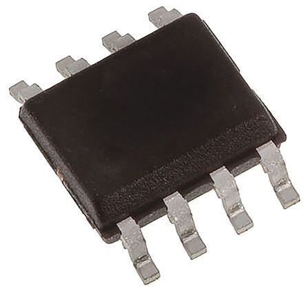
| 描述 | TVS DIODE 6VWM 20VC SOIC8TVS二极管阵列 2 channels telecom/datacom |
| 产品分类 | |
| 品牌 | Littelfuse |
| 产品手册 | |
| 产品图片 |
|
| rohs | 符合RoHS无铅 / 符合限制有害物质指令(RoHS)规范要求 |
| 产品系列 | 二极管与整流器,TVS二极管,TVS二极管阵列,Littelfuse SP03-6BTGSP03-6, SPA® |
| 数据手册 | |
| 产品型号 | SP03-6BTG |
| 不同频率时的电容 | 16pF @ 1MHz |
| 产品培训模块 | http://www.digikey.cn/PTM/IndividualPTM.page?site=cn&lang=zhs&ptm=22970http://www.digikey.cn/PTM/IndividualPTM.page?site=cn&lang=zhs&ptm=24669http://www.digikey.cn/PTM/IndividualPTM.page?site=cn&lang=zhs&ptm=25590 |
| 产品目录绘图 |
|
| 产品目录页面 | |
| 产品种类 | TVS二极管阵列 |
| 供应商器件封装 | 8-SOIC N |
| 其它名称 | F2876DKR |
| 击穿电压 | 6.8 V |
| 功率-峰值脉冲 | 2800W (2.8kW) |
| 包装 | Digi-Reel® |
| 单向通道 | - |
| 双向通道 | 2 |
| 商标 | Littelfuse |
| 商标名 | SPA |
| 安装类型 | 表面贴装 |
| 安装风格 | SMD/SMT |
| 封装 | Reel |
| 封装/外壳 | 8-SOIC(0.154",3.90mm 宽) |
| 封装/箱体 | SOIC-8 |
| 尺寸 | 4 mm W x 5 mm L x 1.65 mm H |
| 峰值浪涌电流 | 150 A |
| 峰值脉冲功率耗散 | 2800 W |
| 工作温度 | -40°C ~ 125°C (TJ) |
| 工作电压 | 6 V |
| 工具箱 | /product-detail/zh/4922864/ETHERNETLF-KIT-ND/2194860 |
| 工厂包装数量 | 2500 |
| 应用 | 以太网 |
| 最大工作温度 | + 125 C |
| 最小工作温度 | - 55 C |
| 极性 | Bidirectional |
| 标准包装 | 1 |
| 特色产品 | http://www.digikey.com/cn/zh/ph/littelfuse/sp03a.html |
| 电压-击穿(最小值) | 6.8V |
| 电压-反向关态(典型值) | 6V (最小值) |
| 电压-箝位(最大值)@Ipp | 20V |
| 电容 | 16 pF |
| 电流-峰值脉冲(10/1000µs) | 150A (8/20µs) |
| 电源线路保护 | 是 |
| 端接类型 | SMD/SMT |
| 类型 | 转向装置(轨至轨) |
| 系列 | SP03-6 |
| 通道 | 2 Channels |
| 钳位电压 | 20 V |


- 商务部:美国ITC正式对集成电路等产品启动337调查
- 曝三星4nm工艺存在良率问题 高通将骁龙8 Gen1或转产台积电
- 太阳诱电将投资9.5亿元在常州建新厂生产MLCC 预计2023年完工
- 英特尔发布欧洲新工厂建设计划 深化IDM 2.0 战略
- 台积电先进制程称霸业界 有大客户加持明年业绩稳了
- 达到5530亿美元!SIA预计今年全球半导体销售额将创下新高
- 英特尔拟将自动驾驶子公司Mobileye上市 估值或超500亿美元
- 三星加码芯片和SET,合并消费电子和移动部门,撤换高东真等 CEO
- 三星电子宣布重大人事变动 还合并消费电子和移动部门
- 海关总署:前11个月进口集成电路产品价值2.52万亿元 增长14.8%


PDF Datasheet 数据手册内容提取
TVS Diode Arrays (SPA® Diodes) Lightning Surge Protection - SP03-6 Series SP03-6 Series 6V 150A Diode Array RoHS Pb GREEN Description This new broadband protection component from Littelfuse provides overvoltage protection for applications such as 10/100/1000 BaseT Ethernet, T3/E3 DS3 interfaces, ADSL2+, and VDSL2+. This new protector combines the TVS diode element with a diode rectifier bridge to provide both longitudinal and differential protection in one package. This design innovation results in a capacitive loading characteristic that is log-linear with respect to the signal voltage across the device. This reduces intermodulation (IM) distortion caused by a typical solid-state protection solution. The application schematic provides the connection information. Agency Approvals Features Agency Agency File Number • RoHS compliant • UL Recognized • SOIC-8 surface mount compound meeting E128662 package (JEDEC MS-012) flammability rating V-0 • Low insertion loss, log- • Lightning, 150A (8/20 as linear capacitance defined in IEC 61000-4-5 2nd edition) Pinout • Combined longitudinal and metallic protection • Low clamping voltage 1 8 • Clamping speed of nanoseconds 2 7 3 6 Applications 4 5 • T1/E1 Line cards • 10/100/1000 BaseT • T3/E3 and DS3 Interfaces Ethernet SOIC-8 (Top View) • STS-1 Interfaces Functional Block Diagram Application Example Pin 1 and 8 Line in Line out TeleLink (0461 1.25) SP03-6 TIP 1 8 Pin 2, 3, 6, and 7 2 7 to chipset (Ethernet PHY, 3 6 T3/E3 PHY, etc.) 4 5 Line in Line out Pin 4 and 5 RING This schematic shows a high-speed data interface Additional Information protection solution. The SP03-6 provides both metallic (differential) and longitudinal (common mode) protection from lightning induced surge events. Its surge rating is compatible with the intra-building surge requirements of Telcordia’s GR-1089-CORE, and the Basic Level Datasheet Resources Samples Recommendations of ITU K.20 and .21. This component protects against both positive and negative induced surge events. The TeleLink fuse provides overcurrent protection Life Support Note: for the long term 50/60 Hz power fault events. Not Intended for Use in Life Support or Life Saving Applications The products shown herein are not designed for use in life sustaining or life saving applications unless otherwise expressly indicated. © 2018 Littelfuse, Inc. Specifications are subject to change without notice. Revised: 12/05/18
TVS Diode Arrays (SPA® Diodes) Lightning Surge Protection - SP03-6 Series Absolute Maximum Ratings Parameter Rating Units Peak Pulse Current (8/20µs) 150 A Peak Pulse Power (8/20µs) 2800 W IEC 61000-4-2, Contact Discharge, (Level 4) 30 kV IEC 61000-4-2, Air Discharge, (Level 4) 30 kV IEC 61000-4-5, 2nd Edition (8/20) 100 A Telcordia GR 1089 (Intra-Building) (2/10µs) 150 A ITU K.20 (5/310µs) 40 A CAUTION: Stresses above those listed in “Absolute Maximum Ratings” may cause permanent damage to the component. This is a stress only rating and operation of the device at these or any other conditions above those indicated in the operational sections of this specification is not implied. Electrical Characteristics (T = 25°C) OP Parameter Symbol Test Conditions Min Typ Max Units Reverse Stand-Off Voltage V - - - 6 V RWM Reverse Breakdown Voltage V I= 1mA 6.8 - - V BR T Reverse Leakage Current I V = 6V, T= 25°C - - 25 µA R RWM Clamping Voltage, Line-Ground V I = 50A, t=8/20 µs - - 15 V C PP p Clamping Voltage, Line-Ground V I = 100A, t=8/20 µs - - 20 V C PP p Between I/O Pins and Ground C (Line-Ground) - 16 25 pF j V =0V, f= 1MHz Junction Capacitance R Between I/O Pins C (Line-Line) - 8 12 pF j V =0V, f= 1MHz R Figure 1: Non-repetitive Peak Pulse Current vs. Pulse Time Figure 2: Current Derating Curve 1000 120 )I%P100 )A( tn100 ( tnerruC 80 erruC esluP kaeP 10 detaR fo egatnecreP 246000 1 0 1 10 100 1000 0 20 40 60 80 100 120 140 160 Pulse decay time (µs) Ambient Temperature (C) © 2018 Littelfuse, Inc. Specifications are subject to change without notice. Revised: 12/05/18
TVS Diode Arrays (SPA® Diodes) Lightning Surge Protection - SP03-6 Series Figure 3: Pulse Waveform Figure 4: Clamping Voltage vs. Peak Pulse Current 25 100 Line-to-Line 20 %) 80 e (V) ntage of I(PP 60 mping Voltag 1150 Line-to-Ground Perce 40 V ClaC 20 5 0 0 0 20 40 60 80 100 0 5 10 15 20 25 30 35 40 Time, µs IP Peak Impulse Current (A) Figure 5: Capacitance vs. Reverse Voltage Figure 6: Forward Voltage vs. Forward Current 20 7 18 Line-to-Ground 6 16 Ground-to-Line )Fp 14 )V( e 5 ( ecnaticapa 11028 Line-to-Line gatloV draw 34 C 6 ro 2 F 4 1 2 0 0 0 1 2 3 4 5 6 7 0 10 20 30 40 50 60 70 80 90 100 Reverse Voltage (V) Forward Current (A) Soldering Parameters Reflow Condition Pb – Free assembly tP TP CCrriittiiccaall ZZoonnee - Temperature Min (Ts(min)) 150°C e RRaammpp--uupp TTLL ttoo TTPP Pre Heat -- TTeimmep e(mraitnu rteo Mmaaxx )( T(ts()max)) 2600 0–° C180 secs rutare TS(mTaxL) tL s pm RRaammpp--ddoown Average ramp up rate (Liquidus) Temp e PPrreehheeaatt 3°C/second max T (TL) to peak TS(min) tS T to T - Ramp-up Rate 3°C/second max S(max) L Reflow -- TTeemmppeerraattuurree ((tTL)) (Liquidus) 26107 –° C1 50 seconds 25 time to peak temperature Time L Peak Temperature (T ) 260+0/-5 °C P Time within 5°C of actual peak 20 – 40 seconds Temperature (t ) p Ramp-down Rate 6°C/second max Time 25°C to peak Temperature (T ) 8 minutes Max. P Do not exceed 260°C © 2018 Littelfuse, Inc. Specifications are subject to change without notice. Revised: 12/05/18
TVS Diode Arrays (SPA® Diodes) Lightning Surge Protection - SP03-6 Series Package Dimensions — Mechanical Drawings and Recommended Solder Pad Outline Package SOIC Pins 8 JEDEC MS-012 Millimetres Inches LF Min Max Min Max A 1.35 1.75 0.053 0.069 o A1 0.10 0.25 0.004 0.010 Recommended A2 1.25 1.65 0.049 0.065 Soldering Pad Outline B 0.31 0.51 0.012 0.020 (Reference Only) c 0.17 0.25 0.007 0.010 D 4.80 5.00 0.189 0.197 E 5.80 6.20 0.228 0.244 E1 3.80 4.00 0.150 0.157 e 1.27 BSC 0.050 BSC L 0.40 1.27 0.016 0.050 Embossed Carrier Tape & Reel Specification — SOIC Package User Feeding Direction Millimetres Inches Min Max Min Max E 1.65 1.85 0.065 0.073 F 5.4 5.6 0.213 0.22 P2 1.95 2.05 0.077 0.081 Pin 1 Location D 1.5 1.6 0.059 0.063 D1 1.50 Min 0.059 Min P0 3.9 4.1 0.154 0.161 10P0 40.0 ± 0.20 1.574 ± 0.008 Part Numbering System W 11.9 12.1 0.468 0.476 P 7.9 8.1 0.311 0.319 SP 03 - 6 B T G A0 6.3 6.5 0.248 0.256 TVS Diode Arrays G= Green B0 5.1 5.3 0.2 0.209 (SPA® Diodes) K0 2 2.2 0.079 0.087 T= Tape & Reel t 0.30 ± 0.05 0.012 ± 0.002 Series Package B - SOIC Working Product Characteristics Voltage Part Marking System Lead Plating Matte Tin Lead Material Copper Alloy Lead Coplanarity 0.003 inches (0.08 mm) LF SP03-6 Substrate Material Silicon XXXXXXXX First Line: Part number Body Material Molded Second Line: Date code UL Recognized compound meeting Flammability flammability rating V-0 Ordering Information Notes : 1. All dimensions are in millimeters 2. Dimensions include solder plating. Part Number Package Marking Min. Order Qty. 3. Dimensions are exclusive of mold flash & metal burr. 4. Blo is facing up for mold and facing down for trim/form, i.e. reverse trim/form. SP03-6BTG SOIC Tape & Reel SP03-6 2500 5. Package surface matte finish VDI 11-13. Disclaimer Notice - Information furnished is believed to be accurate and reliable. However, users should independently evaluate the suitability of and test each product selected for their own applications. Littelfuse products are not designed for, and may not be used in, all applications. Read complete Disclaimer Notice at www.littelfuse.com/disclaimer-electronics. © 2018 Littelfuse, Inc. Specifications are subject to change without notice. Revised: 12/05/18