ICGOO在线商城 > 集成电路(IC) > 接口 - 驱动器,接收器,收发器 > SN75LVDS83CZQLR
 Datasheet下载
- 型号: SN75LVDS83CZQLR
- 制造商: Texas Instruments
- 库位|库存: xxxx|xxxx
- 要求:
| 数量阶梯 | 香港交货 | 国内含税 |
| +xxxx | $xxxx | ¥xxxx |
查看当月历史价格
查看今年历史价格
SN75LVDS83CZQLR产品简介:
ICGOO电子元器件商城为您提供SN75LVDS83CZQLR由Texas Instruments设计生产,在icgoo商城现货销售,并且可以通过原厂、代理商等渠道进行代购。 SN75LVDS83CZQLR价格参考。Texas InstrumentsSN75LVDS83CZQLR封装/规格:接口 - 驱动器,接收器,收发器, 驱动器 5/0 LVDS 56-BGA MICROSTAR JUNIOR(7.0x4.5)。您可以下载SN75LVDS83CZQLR参考资料、Datasheet数据手册功能说明书,资料中有SN75LVDS83CZQLR 详细功能的应用电路图电压和使用方法及教程。
SN75LVDS83CZQLR 是由德州仪器(Texas Instruments)生产的一款低电压差分信号(LVDS)收发器,属于接口 - 驱动器、接收器、收发器类别。以下是其主要应用场景:

1. 高速数据传输:
   SN75LVDS83CZQLR 支持高速数据传输,适用于需要高带宽的应用场景,例如工业自动化设备中的数据通信、医疗设备中的图像传输以及测试测量设备中的信号传递。

2. 显示接口:
   该器件常用于液晶显示器(LCD)、有机发光二极管显示器(OLED)和其他显示屏的接口中,实现从主机到显示屏的高速数据传输,确保清晰流畅的图像显示。

3. 汽车电子系统:
   在汽车行业中,SN75LVDS83CZQLR 可用于车载信息娱乐系统、后视摄像头模块和仪表盘显示等场景,提供可靠的低噪声信号传输,同时满足汽车环境对温度和可靠性的严格要求。

4. 通信设备:
   它可用于通信基站、路由器和交换机等设备中,作为内部或外部组件之间的高速数据链路,确保信号完整性并减少电磁干扰。

5. 嵌入式系统:
   在嵌入式系统中,SN75LVDS83CZQLR 能够连接处理器与外围设备(如传感器、存储器或其他模块),实现高效的数据交换,特别适合需要低功耗和小尺寸设计的应用。

6. 工业控制:
   该收发器适用于工业控制系统中的远程数据采集和监控,例如可编程逻辑控制器(PLC)或分布式控制系统(DCS),通过 LVDS 技术提高抗噪能力和传输距离。

总之,SN75LVDS83CZQLR 凭借其低功耗、高带宽和强抗干扰能力,广泛应用于需要稳定、快速和低噪声信号传输的各种领域。
| 参数 | 数值 |
| 产品目录 | 集成电路 (IC) |
| 描述 | IC FLATLINK TX 10-85MHZ 56BGA |
| 产品分类 | |
| 品牌 | Texas Instruments |
| 数据手册 | |
| 产品图片 |
|
| 产品型号 | SN75LVDS83CZQLR |
| rohs | 无铅 / 符合限制有害物质指令(RoHS)规范要求 |
| 产品系列 | FlatLink™ |
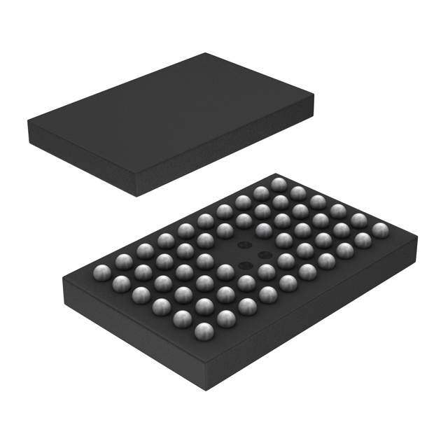
| 供应商器件封装 | 56-BGA MICROSTAR JUNIOR(7.0x4.5) |
| 其它名称 | 296-36729-6 |
| 包装 | Digi-Reel® |
| 协议 | LVDS |
| 双工 | - |
| 安装类型 | 表面贴装 |
| 封装/外壳 | 56-VFBGA |
| 工作温度 | -10°C ~ 70°C |
| 接收器滞后 | - |
| 数据速率 | - |
| 标准包装 | 1 |
| 电压-电源 | 2.8 V ~ 3.6 V |
| 类型 | 驱动器 |
| 驱动器/接收器数 | 5/0 |


- 商务部:美国ITC正式对集成电路等产品启动337调查
- 曝三星4nm工艺存在良率问题 高通将骁龙8 Gen1或转产台积电
- 太阳诱电将投资9.5亿元在常州建新厂生产MLCC 预计2023年完工
- 英特尔发布欧洲新工厂建设计划 深化IDM 2.0 战略
- 台积电先进制程称霸业界 有大客户加持明年业绩稳了
- 达到5530亿美元!SIA预计今年全球半导体销售额将创下新高
- 英特尔拟将自动驾驶子公司Mobileye上市 估值或超500亿美元
- 三星加码芯片和SET,合并消费电子和移动部门,撤换高东真等 CEO
- 三星电子宣布重大人事变动 还合并消费电子和移动部门
- 海关总署:前11个月进口集成电路产品价值2.52万亿元 增长14.8%


PDF Datasheet 数据手册内容提取
SN75LVDS83C www.ti.com SLLSE66A–OCTOBER2010–REVISEDSEPTEMBER2011 FLATLINK™ TRANSMITTER CheckforSamples:SN75LVDS83C FEATURES 1 • LVDSDisplaySerdesInterfacesDirectlyto • 28DataChannelsPlusClockInLow-Voltage 2 LCDDisplayPanelswithIntegratedLVDS TTLto4DataChannelsPlusClockOut • Package:4.5mmx7mmBGA Low-VoltageDifferential • 1.8Vupto3.3VTolerantDataInputsto • ConsumesLessThan1mWWhenDisabled ConnectDirectlytoLow-Power,Low-Voltage • SelectableRisingorFallingClockEdge ApplicationandGraphicProcessors TriggeredInputs • TransferRateupto85Mpps(MegaPixelPer • ESD:5kVHBM Second);PixelClockFrequencyRange10MHz • SupportSpreadSpectrumClocking(SSC) to85MHz • SuitedforDisplayResolutionsRangingFrom APPLICATIONS HVGAuptoHDWithLowEMI • LCDDisplayPanelDriver • OperatesFromaSingle3.3VSupplyand • UMPCandNetbookPC 148mW(typical)at75MHz • DigitalPictureFrame DESCRIPTION The SN75LVDS83C FlatLink™ transmitter contains four 7-bit parallel-load serial-out shift registers, a 7X clock synthesizer, and five Low-Voltage Differential Signaling (LVDS) line drivers in a single integrated circuit. These functions allow 28 bits of single-ended LVTTL data to be synchronously transmitted over five balanced-pair conductorsforreceiptbyacompatiblereceiver,suchastheSN75LVDS82andLCDpanelswithintegratedLVDS receiver. When transmitting, data bits D0 through D27 are each loaded into registers upon the edge of the input clock signal (CLKIN). The rising or falling edge of the clock can be selected via the clock select (CLKSEL) pin. The frequency of CLKIN is multiplied seven times, and then used to unload the data registers in 7-bit slices and serially. The four serial streams and a phase-locked clock (CLKOUT) are then output to LVDS output drivers. ThefrequencyofCLKOUTisthesameastheinputclock,CLKIN. swivel Application processor SN75LVDS83C (e.g. OMAPTM) FlatLinkTMTransmitter BGAPackage: 4.5 x 7mm 1 Pleasebeawarethatanimportantnoticeconcerningavailability,standardwarranty,anduseincriticalapplicationsofTexas Instrumentssemiconductorproductsanddisclaimerstheretoappearsattheendofthisdatasheet. FlatLinkisatrademarkofTexasInstruments. 2 PRODUCTIONDATAinformationiscurrentasofpublicationdate. Copyright©2010–2011,TexasInstrumentsIncorporated Products conform to specifications per the terms of the Texas Instruments standard warranty. Production processing does not necessarilyincludetestingofallparameters.
SN75LVDS83C SLLSE66A–OCTOBER2010–REVISEDSEPTEMBER2011 www.ti.com Thesedeviceshavelimitedbuilt-inESDprotection.Theleadsshouldbeshortedtogetherorthedeviceplacedinconductivefoam duringstorageorhandlingtopreventelectrostaticdamagetotheMOSgates. DESCRIPTION (CONTINUED) The SN75LVDS83C requires no external components and little or no control. The data bus appears the same at the input to the transmitter and output of the receiver with the data transmission transparent to the user(s). The only user intervention is selecting a clock rising edge by inputting a high level to CLKSEL or a falling edge with a low-level input, and the possible use of the Shutdown/Clear (SHTDN). SHTDN is an active-low input to inhibit the clock, and shut off the LVDS output drivers for lower power consumption. A low-level on this signal clears all internalregisterstoalow-level. TheSN75LVDS83Cischaracterizedforoperationoverambientairtemperaturesof-10°Cto70°C. ORDERINGINFORMATION(1) PARTNUMBER PARTMARKING PACKAGE SN75LVDS83CZQLR LVDS83CinBGApackage 56-pinZQLLARGETapeandReel (1) Forthemostcurrentpackageandorderinginformation,seethePackageOptionAddendumlocatedattheendofthisdatasheet,or refertoourwebsiteatwww.ti.com. ABSOLUTE MAXIMUM RATINGS(1) VALUE UNIT MIN MAX Supplyvoltagerange,VCC,IOVCC,LVDSVCC,PLLVCC(2) -0.5 4 V Voltagerangeatanyoutputterminal -0.5 VCC+0.5 V Voltagerangeatanyinputterminal -0.5 IOVCC+0.5 V Continuouspowerdissipation SeetheThermalInformationTable Storagetemperature,T –65 150 °C s HumanBodyModel(HBM)(3)allpins 5 kV ESDrating ChargedDeviceModel(CDM)(4)allpins 500 V MachineModel(MM)(5)allpins 150 V (1) Stressesabovetheseratingsmaycausepermanentdamage.Exposuretoabsolutemaximumconditionsforextendedperiodsmay degradedevicereliability.Thesearestressratingsonly,andfunctionaloperationofthedeviceattheseoranyotherconditionsbeyond thosespecifiedisnotimplied. (2) AllvoltagesarewithrespecttotheGNDterminals. (3) InaccordancewithJEDECStandard22,TestMethodA114-A. (4) InaccordancewithJEDECStandard22,TestMethodC101. (5) InaccordancewithJEDECStandard22,TestMethodA115-A. 2 SubmitDocumentationFeedback Copyright©2010–2011,TexasInstrumentsIncorporated ProductFolderLink(s):SN75LVDS83C
SN75LVDS83C www.ti.com SLLSE66A–OCTOBER2010–REVISEDSEPTEMBER2011 RECOMMENDED OPERATING CONDITIONS overoperatingfree-airtemperaturerange(unlessotherwisenoted) PARAMETER MIN NOM MAX UNIT Supplyvoltage,VCC 2.8 3.3 3.6 LVDSoutputSupplyvoltage,LVDSVCC 2.8 3.3 3.6 PLLanalogsupplyvoltage,PLLVCC 2.8 3.3 3.6 V IOinputreferencesupplyvoltage,IOVCC 1.62 1.8/2.5/3.3 3.6 PowersupplynoiseonanyVCCterminal 0.1 IOVCC=1.8V IOVCC/2+0.3V High-levelinputvoltage,V IOVCC=2.5V IOVCC/2+0.4V V IH IOVCC=3.3V IOVCC/2+0.5V IOVCC=1.8V IOVCC/2-0.3V Low-levelinputvoltage,V IOVCC=2.5V IOVCC/2-0.4V V IL IOVCC=3.3V IOVCC/2-0.5V Differentialloadimpedance,Z 90 132 Ω L Operatingfree-airtemperature,T -10 70 C A THERMAL INFORMATION SN75LVDS83C THERMALMETRIC(1) UNIT ZQL(56PINS) θ Junction-to-ambientthermalresistance 67.1 °C/W JA θ Junction-to-case(top)thermalresistance 25.2 °C/W JCtop θ Junction-to-boardthermalresistance 31.0 °C/W JB ψ Junction-to-topcharacterizationparameter 0.8 °C/W JT ψ Junction-to-boardcharacterizationparameter 30.3 °C/W JB θ Junction-to-case(bottom)thermalresistance n/a °C/W JCbot (1) Formoreinformationabouttraditionalandnewthermalmetrics,seetheICPackageThermalMetricsapplicationreport,SPRA953. TIMING REQUIREMENTS PARAMETER MIN MAX UNIT Inputclockperiod,t 11.76 100 ns c withmodulationfrequency30kHz 8% Inputclockmodulation withmodulationfrequency50kHz 6% High-levelinputclockpulsewidthduration,t 0.4t 0.6t ns w c c Inputsignaltransitiontime,t 3 ns t Datasetuptime,D0throughD27beforeCLKIN(SeeFigure3) 2 ns Dataholdtime,D0throughD27afterCLKIN 0.8 ns Copyright©2010–2011,TexasInstrumentsIncorporated SubmitDocumentationFeedback 3 ProductFolderLink(s):SN75LVDS83C
SN75LVDS83C SLLSE66A–OCTOBER2010–REVISEDSEPTEMBER2011 www.ti.com ZQLPACKAGE (TOPVIEW) 6 5 4 3 2 1 K D8 D7 D5 D4 D2 D1 J D9 GND D6 D3 D0 D27 H D11 VCC D10 GND Y0P Y0M G D13 D12 IOVCC GND Y1P Y1M F D14 GND GND LVDSVCC E D16 D15 Y2P Y2M D D17 D18 CLKSEL GND CLKP CLKM C D19 GND IOVCC GND Y3P Y3M B D20 D21 D25 SHTDN PLLVCC GND A D22 D23 D24 D26 CLKIN GND ZQLPINLIST Ball# Signal Ball# Signal Ball# Signal A1 GND A2 CLKIN A3 D26 A4 D24 A5 D23 A6 D22 B1 GND B2 PLLVCC B3 SHTDN B4 D25 B5 D21 B6 D20 C1 Y3M C2 Y3P C3 GND C4 IOVCC C5 GND C6 D19 D1 CLKM D2 CLKP D3 GND D4 CLKSEL D5 D18 D6 D17 E1 Y2M E2 Y2P E3 ballnotpopulated E4 ballnotpopulated E5 D15 E6 D16 F1 LVDSVCC F2 GND F3 ballnotpopulated F4 ballnotpopulated F5 GND F6 D14 G1 Y1M G2 Y1P G3 GND G4 IOVCC G5 D12 G6 D13 H1 Y0M H2 Y0P H3 GND H4 D10 H5 VCC H6 D11 J1 D27 J2 D0 J3 D3 J4 D6 J5 GND J6 D9 K1 D1 K2 D2 K3 D4 K4 D5 K5 D7 K6 D8 4 SubmitDocumentationFeedback Copyright©2010–2011,TexasInstrumentsIncorporated ProductFolderLink(s):SN75LVDS83C
SN75LVDS83C www.ti.com SLLSE66A–OCTOBER2010–REVISEDSEPTEMBER2011 PINFUNCTIONS PIN I/O DESCRIPTION Y0P,Y0M,Y1P, DifferentialLVDSdataoutputs. Y1M,Y2P,Y2M Outputsarehigh-impedancewhenSHTDNispulledlow(de-asserted) DifferentialLVDSDataoutputs. Y3P,Y3M LVDSOut Outputishigh-impedancewhenSHTDNispulledlow(de-asserted). Note:iftheapplicationonlyrequires18-bitcolor,thisoutputcanbeleftopen. DifferentialLVDSpixelclockoutput. CLKP,CLKM Outputishigh-impedancewhenSHTDNispulledlow(de-asserted). Datainputs;supports1.8Vto3.3VinputvoltageselectablebyVDDsupply.Toconnectagraphic sourcesuccessfullytoadisplay,thebitassignmentofD[27:0]iscritical(andnotnecessarily intuitive). D0–D27 ForinputbitassignmentseeFigure11toFigure14fordetails. Note:ifapplicationonlyrequires18-bitcolor,connectunusedinputsD5,D10,D11,D16,D17,D23, CMOSINwith andD27toGND. CLKIN pulldn Inputpixelclock;risingorfallingclockpolarityisselectablebyControlinputCLKSEL. Deviceshutdown;pulllow(de-assert)toshutdownthedevice(lowpower,resetsallregisters)and SHTDN high(assert)fornormaloperation. Selectsbetweenrisingedgeinputclocktrigger(CLKSEL=V andfallingedgeinputclocktrigger CLKSEL IH (CLKSEL=V ). IL VCC 3.3Vdigitalsupplyvoltage IOVCC I/Osupplyreferencevoltage(1.8Vupto3.3VmatchingtheGPUdataoutputsignalswing) PLLVCC PowerSupply(1) 3.3VPLLanalogsupply LVDSVCC 3.3VLVDSoutputanalogsupply GND SupplygroundforVCC,IOVCC,LVDSVCC,andPLLVCC. (1) Foramultilayerpcb,itisrecommendedtokeeponecommonGNDlayerunderneaththedeviceandconnectallgroundterminals directlytothisplane. Copyright©2010–2011,TexasInstrumentsIncorporated SubmitDocumentationFeedback 5 ProductFolderLink(s):SN75LVDS83C
SN75LVDS83C SLLSE66A–OCTOBER2010–REVISEDSEPTEMBER2011 www.ti.com FUNCTIONALBLOCKDIAGRAM Parallel-Load 7-bit Shift Register D0, D1, D2, D3, 7 Y0P A,B,...G D4, D6, D7 SHIFT/LOAD Y0M >CLK Parallel-Load 7-bit Shift Register D8, D9, D12, D13, 7 Y1P A,B,...G D14, D15, D18 SHIFT/LOAD Y1M >CLK Parallel-Load 7-bit ShiftRegister D19, D20, D21, D22, 7 Y2P A,B,...G D24, D25, D26 SHIFT/LOAD Y2M >CLK Parallel-Load 7-bit Shift Register D27, D5, D10, D11, 7 Y3P A,B,...G D16, D17, D23 SHIFT/LOAD Y3M >CLK Control Logic SHTDN 7X Clock/PLL 7XCLK CLKOUTP CLKIN >CLK CLKOUTM CLKINH CLKSEL RISING/FALLING EDGE 6 SubmitDocumentationFeedback Copyright©2010–2011,TexasInstrumentsIncorporated ProductFolderLink(s):SN75LVDS83C
SN75LVDS83C www.ti.com SLLSE66A–OCTOBER2010–REVISEDSEPTEMBER2011 Dn CLKIN or CLKIN CLKOUT Previous cycle Current cycle Next Y0 D0-1 D7 D6 D4 D3 D2 D1 D0 D7+1 Y1 D8-1 D18 D15 D14 D13 D12 D9 D8 D18+1 Y2 D19-1 D26 D25 D24 D22 D21 D20 D19 D26+1 Y3 D27-1 D23 D17 D16 D11 D10 D5 D27 D23+1 Figure1. TypicalSN75LVDS83CLoadandShiftSequences LVDSVCC IOVCC 5W YnPor D or 50W YnM SHTDN 10kW 7V 300kW 7V Figure2. EquivalentInputandOutputSchematicDiagrams Copyright©2010–2011,TexasInstrumentsIncorporated SubmitDocumentationFeedback 7 ProductFolderLink(s):SN75LVDS83C
SN75LVDS83C SLLSE66A–OCTOBER2010–REVISEDSEPTEMBER2011 www.ti.com ELECTRICAL CHARACTERISTICS overoperatingfree-airtemperaturerange(unlessotherwisenoted) PARAMETER TESTCONDITIONS MIN TYP(1) MAX UNIT VT Inputvoltagethreshold IOVCC/2 V Differentialsteady-stateoutputvoltage mV |VOD| magnitude 250 450 RL=100Ω,SeeFigure4 Changeinthesteady-statedifferential Δ|VOD| outputvoltagemagnitudebetween 1 35 mV oppositebinarystates Steady-statecommon-modeoutput VOC(SS) voltage SeeFigure4 1.125 1.375 V Peak-to-peakcommon-modeoutput tR/F(Dx,CLKin)=1ns VOC(PP) voltage 35 mV IIH High-levelinputcurrent VIH=IOVCC 25 μA IIL Low-levelinputcurrent VIL=0V ±10 μA VOY=0V ±24 mA IOS Short-circuitoutputcurrent VOD=0V ±12 mA IOZ High-impedancestateoutputcurrent VO=0VtoVCC ±20 μA Inputpull-downintegratedresistoronall IOVCC=1.8V 200 Rpdn inputs(Dx,CLKSEL,SHTDN,CLKIN) IOVCC=3.3V 100 kΩ disabled,allinputsatGND; IQ Quiescentcurrent(average) SHTDN=VIL 2 100 μA SHTDN=VIH,RL=100Ω(5places), grayscalepattern(Figure5) VCC=3.3V,fCLK=75MHz I(VCC)+I(PLLVCC)+I(LVDSVCC) 44.9 mA I(IOVCC)withIOVCC=1.8V 0.1 ICC Supplycurrent(average) SHTDN=VIH,RL=100Ω(5places), worst-casepattern(Figure6), VCC=3.3V,fCLK=75MHz I(VCC)+I(PLLVCC)+I(LVDSVCC) 55.1 mA I(IOVCC)withIOVCC=1.8V 0.5 CI Inputcapacitance 2 pF (1) AlltypicalvaluesareatVCC=3.3V,T =25°C. A 8 SubmitDocumentationFeedback Copyright©2010–2011,TexasInstrumentsIncorporated ProductFolderLink(s):SN75LVDS83C
SN75LVDS83C www.ti.com SLLSE66A–OCTOBER2010–REVISEDSEPTEMBER2011 SWITCHING CHARACTERISTICS overoperatingfree-airtemperaturerange(unlessotherwisenoted) PARAMETER TESTCONDITIONS MIN TYP(1) MAX UNIT Delaytime,CLKOUT↑afterYnvalid t (serialbitposition0,equalD1,D9, -0.15 0 0.15 ns 0 D20,D5) Delaytime,CLKOUT↑afterYnvalid t (serialbitposition1,equalD0,D8, 1/ t -0.15 1/ t +0.15 ns 1 7 c 7 c D19,D27) Delaytime,CLKOUT↑afterYnvalid t (serialbitposition2,equalD7,D18, 2/ t -0.15 2/ t +0.15 ns 2 7 c 7 c D26.D23) Delaytime,CLKOUT↑afterYnvalid t3 (serialbitposition3;equalD6,D15, S|InepeuFticgluorcek7ji,ttteCr|=<1235.3pnss(,2) 3/7tc-0.15 3/7tc+0.15 ns D25,D17) Delaytime,CLKOUT↑afterYnvalid t (serialbitposition4,equalD4,D14, 4/ t -0.15 4/ t +0.15 ns 4 7 c 7 c D24,D16) Delaytime,CLKOUT↑afterYnvalid t (serialbitposition5,equalD3,D13, 5/ t -0.15 5/ t +0.15 ns 5 7 c 7 c D22,D11) Delaytime,CLKOUT↑afterYnvalid t (serialbitposition6,equalD2,D12, 6/ t -0.15 6/ t +0.15 ns 6 7 c 7 c D21,D10) t Outputclockperiod t ns c(o) c t =13.3ns;cleanreferenceclock,see C ±26 Figure8 Δt Outputclockcycle-to-cyclejitter (3) ps c(o) t =13.3nswith0.05UIaddednoise C ±44 modulatedat3MHz,seeFigure8 t High-leveloutputclockpulseduration 4/ t ns w 7 c Differentialoutputvoltagetransition t SeeFigure4 200 250 800 ps r/f time(t ort) r f Enabletime,SHTDN↑tophaselock t f =85MHz,SeeFigure9 15 µs en (Ynvalid) (clk) Disabletime,SHTDN↓tooff-state t f =85MHz,SeeFigure10 13 ns dis (CLKOUThigh-impedance) (clk) (1) AlltypicalvaluesareatV =3.3V,T =25°C. CC A (2) |Inputclockjitter|isthemagnitudeofthechangeintheinputclockperiod. (3) Theoutputclockcycle-to-cyclejitteristhelargestrecordedchangeintheoutputclockperiodfromonecycletothenextcycleobserved over15,000cycles.TektronixTDSJIT3JitterAnalysissoftwarewasusedtoderivethemaximumandminimumjittervalue. PARAMETER MEASUREMENT INFORMATION tsu thold Dn CLKIN AllinputtimingisdefinedatIOVDD/2onaninputsignalwitha10%to90%riseorfalltimeoflessthan3ns. CLKSEL=0V. Figure3. SetUpandHoldTimeDefinition Copyright©2010–2011,TexasInstrumentsIncorporated SubmitDocumentationFeedback 9 ProductFolderLink(s):SN75LVDS83C
SN75LVDS83C SLLSE66A–OCTOBER2010–REVISEDSEPTEMBER2011 www.ti.com PARAMETER MEASUREMENT INFORMATION (continued) 49.9W± 1% (2 PLCS) YP V OD YM VOC 100% 80% V OD(H) 0V V OD(L) 20% 0% t t f r V OC(PP) V V OC(SS) OC(SS) 0V Figure4. TestLoadandVoltageDefinitionsforLVDSOutputs. CLKIN D0,8,16 D1,9,17 D2,10,18 D3,11,19 D4-7,12-15,20-23 D24-27 The16grayscaletestpatterntestdevicepowerconsumptionforatypicaldisplaypattern. Figure5. 16GrayscaleTestPattern 10 SubmitDocumentationFeedback Copyright©2010–2011,TexasInstrumentsIncorporated ProductFolderLink(s):SN75LVDS83C
SN75LVDS83C www.ti.com SLLSE66A–OCTOBER2010–REVISEDSEPTEMBER2011 PARAMETER MEASUREMENT INFORMATION (continued) T CLKIN EVEN Dn ODD Dn Theworst-casetestpatternproducesnearlythemaximumswitchingfrequencyforalloftheLVDSoutputs. Figure6. Worst-CasePowerTestPattern t 7 CLKIN CLKOUT t 6 t 5 t 4 t 3 t 2 t 1 t 0 Yn V OD(H) ~2.5V CLKOUT orYn 0.00V 1.40V CLKIN ~0.5V V OD(L) t7 t0-6 CLKOUTisshownwithCLKSELathigh-level. CLKINpolaritydependsonCLKSELinputlevel. Figure7. SN75LVDS83CTimingDefinitions Copyright©2010–2011,TexasInstrumentsIncorporated SubmitDocumentationFeedback 11 ProductFolderLink(s):SN75LVDS83C
SN75LVDS83C SLLSE66A–OCTOBER2010–REVISEDSEPTEMBER2011 www.ti.com PARAMETER MEASUREMENT INFORMATION (continued) Device + Reference VCO Under Test + Modulation v(t) =Asin(2pf t) mod HP8656B Signal HP8665ASynthesized Device Under DTS2070C Generator, Signal Generator, Test Digital 0.1 MHz-990 MHz 0.1 MHz-4200 MHz TimeScope RF Output CLKIN CLKOUT Input RF Output Modulation Input Figure8. OutputClockJitterTestSetUp CLKIN Dn ten SHTDN Invalid Yn Valid Figure9. EnableTimeWaveforms CLKIN tdis SHTDN CLKOUT Figure10. DisableTimeWaveforms 12 SubmitDocumentationFeedback Copyright©2010–2011,TexasInstrumentsIncorporated ProductFolderLink(s):SN75LVDS83C
SN75LVDS83C www.ti.com SLLSE66A–OCTOBER2010–REVISEDSEPTEMBER2011 APPLICATION INFORMATION This section describes the power up sequence, provides information on device connectivity to various GPU and LCDdisplaypanels,andoffersapcbroutingexample. Power Up Sequence TheSN75LVDS83Cdoesnotrequireaspecificpowerupsequence. It is permitted to power up IOVCC while VCC, VCCPLL, and VCCLVDS remain powered down and connected to GND. The input level of the SHTDN during this time does not matter as only the input stage is powered up while allotherdeviceblocksarestillpowereddown. It is also permitted to power up all 3.3V power domains while IOVCC is still powered down to GND. The device will not suffer damage. However, in this case, all the I/Os are detected as logic HIGH, regardless of their true input voltage level. Hence, connecting SHTDN to GND will still be interpreted as a logic HIGH; the LVDS output stage will turn on. The power consumption in this condition is significantly higher than standby mode, but still lowerthannormalmode. The user experience can be impacted by the way a system powers up and powers down an LCD screen. The followingsequenceisrecommended: Powerupsequence(SN75LVDS83CSHTDNinputinitiallylow): 1. RampupLCDpower(maybe0.5msto10ms)butkeepbacklightturnedoff. 2. Waitforadditional0-200mstoensuredisplaynoisewon’toccur. 3. Enablevideosourceoutput;startsendingblackvideodata. 4. ToggleLVDS83CshutdowntoSHTDN=V . IH 5. Send >1ms of black video data; this allows the LVDS83C to be phase locked, and the display to show black datafirst. 6. Startsendingtrueimagedata. 7. Enablebacklight. PowerDownsequence(SN75LVDS83CSHTDNinputinitiallyhigh): 1. DisableLCDbacklight;waitfortheminimumtimespecifiedintheLCDdatasheetforthebacklighttogolow. 2. Video source output data switch from active video data to black image data (all visible pixel turn black); drive thisfor>2frametimes. 3. SetSN75LVDS83CinputSHTDN=GND;waitfor250ns. 4. Disablethevideooutputofthevideosource. 5. RemovepowerfromtheLCDpanelforlowestsystempower. Signal Connectivity While there is no formal industry standardized specification for the input interface of LVDS LCD panels, the industry has aligned over the years on a certain data format (bit order). Figure 11 through Figure 14 show how each signal should be connected from the graphic source through the SN75LVDS83C input, output and LVDS LCDpanelinput.Detailednotesareprovidedwitheachfigure. Copyright©2010–2011,TexasInstrumentsIncorporated SubmitDocumentationFeedback 13 ProductFolderLink(s):SN75LVDS83C
SN75LVDS83C SLLSE66A–OCTOBER2010–REVISEDSEPTEMBER2011 www.ti.com 24-bpc GPU SN75LVDS83C FORMAT1 FORMAT2 (See NoteA) R0(LSB) D0 D27 R1 D1 D5 R2 D2 D0 R3 D3 D1 R4 D4 D2 Y0M 100 R5 D6 D3 Y0P R6 D27 D4 to column R7(MSB) D5 D6 Y1M driver 100 G0(LSB) D7 D10 Y1P GGGGG12345 DDDDD89111234 DDDDD1789112 YYY232MMP Main board connectorCFaPbClePanel connector 10(80bCpotLcinmV,t Dr2ino4Sgllbeprp) G6 D10 D13 Y3P 100 to row driver G7(LSB) D11 D14 B0(LSB) D15 D16 CLKOUTM B1 D18 D17 CLKOUTP 100 B2 D19 D15 B3 D20 D18 B4 D21 D19 24-bpp LCD Display B5 D22 D20 B6 D16 D21 B7(MSB) D17 D22 HSYNC D24 D24 VSYNC D25 D25 ENABLE D26 D26 RSVD (Note C) D23 D23 O CLK CLKIN CLKIN C GND VDDIGPU IOVCC SHTDN CLKSEL GND VCCPLLVCCLVDSVC 4.8k 3.3V 3.3V 1.8oVr 3o.r3 2V.5V C1 Rpullup C2 C3 Rpulldown (See Note B) Main Board NoteA.FORMAT:Themajorityof24-bitLCDdisplaypanelsrequirethetwomostsignificantbits(2MSB)ofeach colortobetransferredoverthe4thserialdataoutputY3.Afew24-bitLCDdisplaypanelsrequirethetwoLSBsof eachcolortobetransmittedovertheY3output.Thesystemdesignerneedstoverifywhichformatisexpectedby checkingtheLCDdisplaydatasheet. • Format 1: use with displays expecting the 2 MSB to be transmitted over the 4th data channel Y3. This is the dominatedataformatforLCDpanels. • Format2:usewithdisplaysexpectingthe2LSBtobetransmittedoverthe4thdatachannel. NoteB.Rpullup:installonlytouserisingedgetriggeredclocking. Rpulldown:installonlytousefallingedgetriggeredclocking. • C1:decouplingcapfortheVDDIOsupply;installatleast1x0.01µF. • C2:decouplingcapfortheVDDsupply;installatleast1x0.1µFand1x0.01µF. • C3:decouplingcapfortheVDDPLLandVDDLVDSsupply;installatleast1x0.1µFand1x0.01µF. NoteC.IfRSVDisnotdriventoavalidlogiclevel,thenanexternalconnectiontoGNDisrecommended. NoteD.RSVDmustbedriventoavalidlogiclevel.AllunusedSN75LVDS83Cinputsmustbetiedtoavalidlogic level. Figure11. 24-BitColorHostto24-bitLCDPanelApplication 14 SubmitDocumentationFeedback Copyright©2010–2011,TexasInstrumentsIncorporated ProductFolderLink(s):SN75LVDS83C
SN75LVDS83C www.ti.com SLLSE66A–OCTOBER2010–REVISEDSEPTEMBER2011 18-bpp GPU SN75LVDS83C R0(LSB) D0 R1 D1 R2 D2 R3 D3 R4 D4 Y0M 100 R5(MSB) D6 Y0P D27 to column driver D5 Y1M 100 G0(LSB) D7 Y1P G5(MSGGGGB1234) DDDDD89111234 CLKOUYYT22MMP Main board connectorCFaPbClePanel connector (160-0bCpotLcinmV,t Dr1ino8Sgll-ebrpp) 100 D10 CLKOUTP to row driver D11 B0(LSB) D15 B1 D18 B2 D19 B3 D20 B4 D21 18-bpp LCD Display B5(MSB) D22 D16 D17 Y3M HSYNC D24 Y3P (See NoteA) VSYNC D25 ENABLE D26 RSVD D23 O CLK CLKIN C GND VDIDGPU IOVCC SHTDN CLKSEL GND VCCPLLVCCLVDSVC 4.8k 3.3V 3.3V 1.8V or 2.5V C1 Rpullup C2 C3 or 3.3V Rpulldown (See Note B) Main Board NoteA.LeaveoutputY3NC. NoteB.Rpullup:installonlytouserisingedgetriggeredclocking. Rpulldown:installonlytousefallingedgetriggeredclocking. • C1:decouplingcapfortheVDDIOsupply;installatleast1x0.01µF. • C2:decouplingcapfortheVDDsupply;installatleast1x0.1µFand1x0.01µF. • C3:decouplingcapfortheVDDPLLandVDDLVDSsupply;installatleast1x0.1µFand1x0.01µF. Figure12. 18-BitColorHostto18-BitColorLCDPanelDisplayApplication Copyright©2010–2011,TexasInstrumentsIncorporated SubmitDocumentationFeedback 15 ProductFolderLink(s):SN75LVDS83C
SN75LVDS83C SLLSE66A–OCTOBER2010–REVISEDSEPTEMBER2011 www.ti.com 12-bpp GPU SN75LVDS83C (See Note B) R2or VCC D0 R3or GND D1 R0 D2 R1 D3 R2 D4 Y0M 100 R3(MSB) D6 Y0P D27 to column driver (See Note B) D5 Y1M 100 G2or VCC D7 Y1P GG33(oMr GSGGGNB012D) DDDDD89111234 CLKOUYYT22MMP Main board connectorCFaPbCleltPanel connector (610-bC0poLtcinVm,t Dr1ion8Slgl-ebrpp) 100 D10 CLKOUTP to row driver (See Note B) D11 B2or VCC D15 B3or GND D18 B0 D19 B1 D20 B2 D21 18-bpp LCD Display B3(MSB) D22 D16 D17 Y3M HSYNC D24 Y3P (See NoteA) VSYNC D25 ENABLE D26 RSVD D23 O CLK CLKIN C GND VDDIGPU IOVCC SHTDN CLKSEL GND VCCPLLVCCLVDSVC 4.8k 3.3V 3.3V 1.8V or 2.5V C1 Rpullup C2 C3 or 3.3V Rpulldown (See Note C) Main Board NoteA.LeaveoutputY3N.C. NoteB.R3,G3,B3:thisMSBofeachcoloralsoconnectstothe5thbitofeachcolorforincreaseddynamicrangeof theentirecolorspaceattheexpenseofnone-linearstepsizesbetweeneachstep.Forlinearstepswithlessdynamic range,connectD1,D8,andD18toGND. R2,G2,B2:theseoutputsalsoconnectstotheLSBofeachcolorforincreased,dynamicrangeoftheentirecolor spaceattheexpenseofnone-linearstepsizesbetweeneachstep.Forlinearstepswithlessdynamicrange,connect D0,D7,andD15toVCC. NoteC.Rpullup:installonlytouserisingedgetriggeredclocking. Rpulldown:installonlytousefallingedgetriggeredclocking. • C1:decouplingcapfortheVDDIOsupply;installatleast1x0.01µF. • C2:decouplingcapfortheVDDsupply;installatleast1x0.1µFand1x0.01µF. • C3:decouplingcapfortheVDDPLLandVDDLVDSsupply;installatleast1x0.1µFand1x0.01µF. Figure13. 12-BitColorHostto18-BitColorLCDPanelDisplayApplication 16 SubmitDocumentationFeedback Copyright©2010–2011,TexasInstrumentsIncorporated ProductFolderLink(s):SN75LVDS83C
SN75LVDS83C www.ti.com SLLSE66A–OCTOBER2010–REVISEDSEPTEMBER2011 24-bpp GPU SN75LVDS83C R0 and R1: NC R2 D0 (See Note B) R3 D1 R4 D2 R5 D3 R6 D4 Y0M 100 R7(MSB) D6 Y0P D27 to column G(S0e ea nNdo Gte1 B: )NC D5 Y1M 100 driver G2 D7 Y1P G7(MSGGGGB3456) DDDDD89111234 CLKOUYYT22MMP Main board connectorCFaPbCleltPanel connector (610-bC0poLtcinVm,t Dr1ion8Slgl-ebrpp) 100 D10 CLKOUTP to row driver B0 and B1: NC D11 (See Note B) B2 D15 B3 D18 B4 D19 B5 D20 B6 D21 18-bpp LCD Display B7(MSB) D22 D16 B0 and B1: NC (See Note B) D17 Y3M HSYNC D24 Y3P (See NoteA) VSYNC D25 ENABLE D26 RSVD D23 O CLK CLKIN C GND VDDIGPU IOVCC SHTDN CLKSEL GND VCCPLLVCCLVDSVC 4.8k 3.3V 3.3V 1.8V or 2.5V C1 Rpullup C2 C3 or 3.3V Rpulldown (See Note C) Main Board NoteA.LeaveoutputY3NC. NoteB.R0,R1,G0,G1,B0,B1:Forimprovedimagequality,theGPUshouldditherthe24-bitoutputpixeldown to18-bitperpixel. NoteC.Rpullup:installonlytouserisingedgetriggeredclocking. Rpulldown:installonlytousefallingedgetriggeredclocking. • C1:decouplingcapfortheVDDIOsupply;installatleast1x0.01µF. • C2:decouplingcapfortheVDDsupply;installatleast1x0.1µFand1x0.01µF. • C3:decouplingcapfortheVDDPLLandVDDLVDSsupply;installatleast1x0.1µFand1x0.01µF. Figure14. 24-BitColorHostto18-BitColorLCDPanelDisplayApplication Copyright©2010–2011,TexasInstrumentsIncorporated SubmitDocumentationFeedback 17 ProductFolderLink(s):SN75LVDS83C
SN75LVDS83C SLLSE66A–OCTOBER2010–REVISEDSEPTEMBER2011 www.ti.com Typical Application Schematic Figure15representstheschematicdrawingoftheSN75LVDS83Cevaluationmodule. J1 U1H C3 sma_surface J2 GND1 C5 GND2 D3 LLVVPDDLSSGGGGGLGGGNNNNNNNDDDDDNDD34567D12 ABFFGHJ2551133 U1ACCYYLL00KKMPMP DDHH1212 sma_suJrf3ace sma_suJrf4ace SN75LVDS83CZQL Y1P GG12 J5 sma_surface Y1M E1 Y2P Y2M E2 sma_surface J6 IOVCC C2 R4 R5 R6 R7 R8 R9 R10 Y3P C1 4.7k 4.7k 4.7k 4.7k 4.7k 4.7k 4.7k Y3M J7 sma_surface U1B JMP1 SN75LVDS83CZQL J2 D0 DD01 KK12 DD21 1 2 sma_surface J8 D2 J3 D3 D3 K3 D4 DD64 JK45 DD67 J9 sma_surface D7 14 Header7x2 SN75LVDS83CZQL IOVCC sma_surface J10 R11 R12 R13 R14 R15 R16 R17 4.7k 4.7k 4.7k 4.7k 4.7k 4.7k 4.7k U1C JMP2 sma_surface K6 D8 D8 J6 D9 1 2 D9 G5 D12 IOVCC IOVCC D12 G6 D13 D13 F6 D14 D14 E5 D15 D15 D5 D18 D18 14 R1 R2 SN75LVDS83CZQL Header7x2 4.7k IOVCC R18 R19 R20 R21 R22 R23 R24 4.7k 4.7k 4.7k 4.7k 4.7k 4.7k 4.7k U1G JMP6 U1DD19 BC66 DD1290 JM1P32 CSLHKTSDENL BD34 SCHLKTDSNEL 13 24 D20 B5 D21 Header2x2 D21 A6 D22 SN75LVDS83CZQL D22 A4 D24 D24 B4 D25 D25 A3 D26 D26 14 U1J E3 Header7x2 NC1 E4 SN75LVDS83CZQL NC2 F3 NC3 F4 NC4 IOVCC R25 R26 R27 R28 R29 R30 R31 SN75LVDS83CZQL 4.7k 4.7k 4.7k 4.7k 4.7k 4.7k 4.7k U1E JMP4 K4 D5 D5 H4 D10 1 2 VCC IOVCC D10 H6 D11 U1I DD1116 DE66 DD1176 PLLVVCCCC BG24 DD2137 AJ15 DD2273 LVDSVCC F1 D27 14 H5 IOVCC1 C4 Header7x2 IOVCC2 SN75LVDS83CZQL SN75LVDS83CZQL VCC VCC VCC IOVCC C31 C32 C33 C34 C35 C36 C40 C41 C42 C37 C38 C39 1uF 0.1uF 0.01uF 1uF 0.1uF 0.01uF 1uF 0.1uF 0.01uF 1uF 0.1uF 0.01uF PLACE UNDER LVDS83C (bottom pcb side) Figure15. SchematicExample(SN75LVDS83CEvaluationBoard) 18 SubmitDocumentationFeedback Copyright©2010–2011,TexasInstrumentsIncorporated ProductFolderLink(s):SN75LVDS83C
SN75LVDS83C www.ti.com SLLSE66A–OCTOBER2010–REVISEDSEPTEMBER2011 PCB Routing Figure16andFigure17showapossiblebreakoutofthedatainputandoutputsignalsfromtheBGApackage. R1 R2 R3 R4 R5 R6 R7 R8 G0 G1 D8 D7 D5 D4 D2 D1 G2 D9 GND D6 D3 D0 D27 G3 D11 VCC D10 GND Y0P Y0M G4 G5 D13 D12 IOVCC GND Y1P Y1M G6 G7 B0 D14 GND LVDSGNDLVDSVCC B1 D16 D15 Y2P Y2M D17 D18 CLKSEL GND CLKP CLKM B2 D19 GND IOVCC GND Y3P Y3M B3 B4 D20 D21 D25 SHTDN PLLVCC LVDSGND +PLL GND B5 B6 D22 D23 D24 D26 CLKIN PLL GND B7 HS VS EN CLK Figure16. 24-BitColorRouting(SeeFigure11fortheSchematic) Copyright©2010–2011,TexasInstrumentsIncorporated SubmitDocumentationFeedback 19 ProductFolderLink(s):SN75LVDS83C
SN75LVDS83C SLLSE66A–OCTOBER2010–REVISEDSEPTEMBER2011 www.ti.com G1 G0 R5 R4 R3 R2 R1 R0 D8 D7 D5 D4 D2 D1 G2 To GND D9 GND D6 D3 D0 D27 D11 VCC D10 GND Y0P Y0M G3 G4 D13 D12 IOVCC GND Y1P Y1M G5 D14 GND LVDS LVDS B0 GND VCC To GND D16 D15 Y2P Y2M B1 D17 D18 CLKSEL GND CLKP CLKM B2 D19 GND IOVCC GND Y3P Y3M remains unconnected B3 D20 D21 D25 SHTDN PLLVCC LVDS B4 GND CLKIN +PLLGND B5 D22 D23 D24 D26 PLL GND HS VS EN CLK Figure17. 18-BitColorRouting(SeeFigure12,Figure13,andFigure14fortheSchematic) 20 SubmitDocumentationFeedback Copyright©2010–2011,TexasInstrumentsIncorporated ProductFolderLink(s):SN75LVDS83C
SN75LVDS83C www.ti.com SLLSE66A–OCTOBER2010–REVISEDSEPTEMBER2011 REVISION HISTORY ChangesfromOriginal(May2009)toRevisionA Page • Multiplychangesthroughoutthedatasheet ......................................................................................................................... 1 Copyright©2010–2011,TexasInstrumentsIncorporated SubmitDocumentationFeedback 21 ProductFolderLink(s):SN75LVDS83C
PACKAGE OPTION ADDENDUM www.ti.com 30-Dec-2019 PACKAGING INFORMATION Orderable Device Status Package Type Package Pins Package Eco Plan Lead/Ball Finish MSL Peak Temp Op Temp (°C) Device Marking Samples (1) Drawing Qty (2) (6) (3) (4/5) HPA02273ZQLR LIFEBUY BGA ZQL 56 1000 Green (RoHS SNAGCU Level-2-260C-1 YEAR 0 to 0 LVDS83C MICROSTAR & no Sb/Br) JUNIOR SN75LVDS83CZQLR LIFEBUY BGA ZQL 56 1000 Green (RoHS SNAGCU Level-2-260C-1 YEAR 0 to 0 LVDS83C MICROSTAR & no Sb/Br) JUNIOR (1) The marketing status values are defined as follows: ACTIVE: Product device recommended for new designs. LIFEBUY: TI has announced that the device will be discontinued, and a lifetime-buy period is in effect. NRND: Not recommended for new designs. Device is in production to support existing customers, but TI does not recommend using this part in a new design. PREVIEW: Device has been announced but is not in production. Samples may or may not be available. OBSOLETE: TI has discontinued the production of the device. (2) RoHS: TI defines "RoHS" to mean semiconductor products that are compliant with the current EU RoHS requirements for all 10 RoHS substances, including the requirement that RoHS substance do not exceed 0.1% by weight in homogeneous materials. Where designed to be soldered at high temperatures, "RoHS" products are suitable for use in specified lead-free processes. TI may reference these types of products as "Pb-Free". RoHS Exempt: TI defines "RoHS Exempt" to mean products that contain lead but are compliant with EU RoHS pursuant to a specific EU RoHS exemption. Green: TI defines "Green" to mean the content of Chlorine (Cl) and Bromine (Br) based flame retardants meet JS709B low halogen requirements of <=1000ppm threshold. Antimony trioxide based flame retardants must also meet the <=1000ppm threshold requirement. (3) MSL, Peak Temp. - The Moisture Sensitivity Level rating according to the JEDEC industry standard classifications, and peak solder temperature. (4) There may be additional marking, which relates to the logo, the lot trace code information, or the environmental category on the device. (5) Multiple Device Markings will be inside parentheses. Only one Device Marking contained in parentheses and separated by a "~" will appear on a device. If a line is indented then it is a continuation of the previous line and the two combined represent the entire Device Marking for that device. (6) Lead/Ball Finish - Orderable Devices may have multiple material finish options. Finish options are separated by a vertical ruled line. Lead/Ball Finish values may wrap to two lines if the finish value exceeds the maximum column width. Important Information and Disclaimer:The information provided on this page represents TI's knowledge and belief as of the date that it is provided. TI bases its knowledge and belief on information provided by third parties, and makes no representation or warranty as to the accuracy of such information. Efforts are underway to better integrate information from third parties. TI has taken and continues to take reasonable steps to provide representative and accurate information but may not have conducted destructive testing or chemical analysis on incoming materials and chemicals. TI and TI suppliers consider certain information to be proprietary, and thus CAS numbers and other limited information may not be available for release. Addendum-Page 1
PACKAGE OPTION ADDENDUM www.ti.com 30-Dec-2019 In no event shall TI's liability arising out of such information exceed the total purchase price of the TI part(s) at issue in this document sold by TI to Customer on an annual basis. Addendum-Page 2
PACKAGE MATERIALS INFORMATION www.ti.com 12-Feb-2019 TAPE AND REEL INFORMATION *Alldimensionsarenominal Device Package Package Pins SPQ Reel Reel A0 B0 K0 P1 W Pin1 Type Drawing Diameter Width (mm) (mm) (mm) (mm) (mm) Quadrant (mm) W1(mm) SN75LVDS83CZQLR BGAMI ZQL 56 1000 330.0 16.4 4.8 7.3 1.5 8.0 16.0 Q1 CROSTA RJUNI OR PackMaterials-Page1
PACKAGE MATERIALS INFORMATION www.ti.com 12-Feb-2019 *Alldimensionsarenominal Device PackageType PackageDrawing Pins SPQ Length(mm) Width(mm) Height(mm) SN75LVDS83CZQLR BGAMICROSTAR ZQL 56 1000 350.0 350.0 43.0 JUNIOR PackMaterials-Page2
PACKAGE OUTLINE ZQL0056A JRBGA - 1 mm max height SCALE 2.100 PLASTIC BALL GRID ARRAY 4.6 B A 4.4 BALL A1 CORNER 7.1 6.9 1 MAX C SEATING PLANE 0.35 0.15 TYP BALL TYP 0.1 C 3.25 TYP SYMM (0.625) TYP K J (0.575) TYP H G 5.85 F SYMM TYP E D C 0.45 56X NOTE 3 0.35 B 0.15 C B A 0.08 C A 0.65 TYP 1 2 3 4 5 6 BALL A1 CORNER 0.65 TYP 4219711/B 01/2017 NOTES: 1. All linear dimensions are in millimeters. Any dimensions in parenthesis are for reference only. Dimensioning and tolerancing per ASME Y14.5M. 2. This drawing is subject to change without notice. 3. No metal in this area, indicates orientation. www.ti.com
EXAMPLE BOARD LAYOUT ZQL0056A JRBGA - 1 mm max height PLASTIC BALL GRID ARRAY (0.65) TYP 56X ( 0.33) 1 2 3 4 5 6 A (0.65) TYP B C D E SYMM F G H J K SYMM LAND PATTERN EXAMPLE EXPOSED METAL SHOWN SCALE:15X SOLDER MASK 0.05 MAX 0.05 MIN METAL UNDER OPENING SOLDER MASK EXPOSED METAL ( 0.33) ( 0.33) METAL EXPOSED METAL SOLDER MASK OPENING NON-SOLDER MASK SOLDER MASK DEFINED DEFINED (PREFERRED) SOLDER MASK DETAILS NOT TO SCALE 4219711/B 01/2017 NOTES: (continued) 4. Final dimensions may vary due to manufacturing tolerance considerations and also routing constraints. For information, see Texas Instruments literature number SPRAA99 (www.ti.com/lit/spraa99). www.ti.com
EXAMPLE STENCIL DESIGN ZQL0056A JRBGA - 1 mm max height PLASTIC BALL GRID ARRAY 56X ( 0.33) (0.65) TYP 1 2 3 4 5 6 A (0.65) TYP B C D E SYMM F G H J K SYMM SOLDER PASTE EXAMPLE BASED ON 0.125 mm THICK STENCIL SCALE:15X 4219711/B 01/2017 NOTES: (continued) 5. Laser cutting apertures with trapezoidal walls and rounded corners may offer better paste release. www.ti.com
IMPORTANTNOTICEANDDISCLAIMER TIPROVIDESTECHNICALANDRELIABILITYDATA(INCLUDINGDATASHEETS),DESIGNRESOURCES(INCLUDINGREFERENCE DESIGNS),APPLICATIONOROTHERDESIGNADVICE,WEBTOOLS,SAFETYINFORMATION,ANDOTHERRESOURCES“ASIS” ANDWITHALLFAULTS,ANDDISCLAIMSALLWARRANTIES,EXPRESSANDIMPLIED,INCLUDINGWITHOUTLIMITATIONANY IMPLIEDWARRANTIESOFMERCHANTABILITY,FITNESSFORAPARTICULARPURPOSEORNON-INFRINGEMENTOFTHIRD PARTYINTELLECTUALPROPERTYRIGHTS. TheseresourcesareintendedforskilleddevelopersdesigningwithTIproducts.Youaresolelyresponsiblefor(1)selectingtheappropriate TIproductsforyourapplication,(2)designing,validatingandtestingyourapplication,and(3)ensuringyourapplicationmeetsapplicable standards,andanyothersafety,security,orotherrequirements.Theseresourcesaresubjecttochangewithoutnotice.TIgrantsyou permissiontousetheseresourcesonlyfordevelopmentofanapplicationthatusestheTIproductsdescribedintheresource.Other reproductionanddisplayoftheseresourcesisprohibited.NolicenseisgrantedtoanyotherTIintellectualpropertyrightortoanythird partyintellectualpropertyright.TIdisclaimsresponsibilityfor,andyouwillfullyindemnifyTIanditsrepresentativesagainst,anyclaims, damages,costs,losses,andliabilitiesarisingoutofyouruseoftheseresources. TI’sproductsareprovidedsubjecttoTI’sTermsofSale(www.ti.com/legal/termsofsale.html)orotherapplicabletermsavailableeitheron ti.comorprovidedinconjunctionwithsuchTIproducts.TI’sprovisionoftheseresourcesdoesnotexpandorotherwisealterTI’sapplicable warrantiesorwarrantydisclaimersforTIproducts. MailingAddress:TexasInstruments,PostOfficeBox655303,Dallas,Texas75265 Copyright©2019,TexasInstrumentsIncorporated