ICGOO在线商城 > 集成电路(IC) > 接口 - 驱动器,接收器,收发器 > SN75ALS181NSR
 Datasheet下载
- 型号: SN75ALS181NSR
- 制造商: Texas Instruments
- 库位|库存: xxxx|xxxx
- 要求:
| 数量阶梯 | 香港交货 | 国内含税 |
| +xxxx | $xxxx | ¥xxxx |
查看当月历史价格
查看今年历史价格
SN75ALS181NSR产品简介:
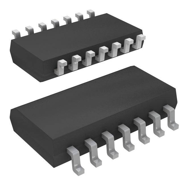
ICGOO电子元器件商城为您提供SN75ALS181NSR由Texas Instruments设计生产,在icgoo商城现货销售,并且可以通过原厂、代理商等渠道进行代购。 SN75ALS181NSR价格参考。Texas InstrumentsSN75ALS181NSR封装/规格:接口 - 驱动器,接收器,收发器, 全 收发器 1/1 RS422,RS485 14-SOP。您可以下载SN75ALS181NSR参考资料、Datasheet数据手册功能说明书,资料中有SN75ALS181NSR 详细功能的应用电路图电压和使用方法及教程。
| 参数 | 数值 |
| 产品目录 | 集成电路 (IC)半导体 |
| 描述 | IC DIFF DRVR/RCVR PRS 14SORS-422/RS-485 接口 IC Diff Pairs |
| Duplex | Full Duplex |
| 产品分类 | |
| 品牌 | Texas Instruments |
| 产品手册 | |
| 产品图片 |
|
| rohs | 符合RoHS无铅 / 符合限制有害物质指令(RoHS)规范要求 |
| 产品系列 | 接口 IC,RS-422/RS-485 接口 IC,Texas Instruments SN75ALS181NSR- |
| 数据手册 | |
| 产品型号 | SN75ALS181NSR |
| 产品目录页面 | |
| 产品种类 | RS-422/RS-485 接口 IC |
| 供应商器件封装 | 14-SO |
| 其它名称 | 296-9963-2 |
| 功能 | Transceiver |
| 包装 | 带卷 (TR) |
| 协议 | RS422,RS485 |
| 单位重量 | 208.300 mg |
| 双工 | 全 |
| 商标 | Texas Instruments |
| 安装类型 | 表面贴装 |
| 安装风格 | SMD/SMT |
| 封装 | Reel |
| 封装/外壳 | 14-SOIC(0.209",5.30mm 宽) |
| 封装/箱体 | SOP-14 |
| 工作温度 | 0°C ~ 70°C |
| 工作温度范围 | 0 C to + 70 C |
| 工作电源电压 | 5 V |
| 工厂包装数量 | 2000 |
| 接收器滞后 | 60mV |
| 接收机数量 | 1 Receiver |
| 数据速率 | - |
| 最大工作温度 | + 70 C |
| 最小工作温度 | 0 C |
| 标准包装 | 2,000 |
| 激励器数量 | 1 Driver |
| 电压-电源 | 4.75 V ~ 5.25 V |
| 电源电流 | 30 mA |
| 类型 | 收发器 |
| 系列 | SN75ALS181 |
| 驱动器/接收器数 | 1/1 |


- 商务部:美国ITC正式对集成电路等产品启动337调查
- 曝三星4nm工艺存在良率问题 高通将骁龙8 Gen1或转产台积电
- 太阳诱电将投资9.5亿元在常州建新厂生产MLCC 预计2023年完工
- 英特尔发布欧洲新工厂建设计划 深化IDM 2.0 战略
- 台积电先进制程称霸业界 有大客户加持明年业绩稳了
- 达到5530亿美元!SIA预计今年全球半导体销售额将创下新高
- 英特尔拟将自动驾驶子公司Mobileye上市 估值或超500亿美元
- 三星加码芯片和SET,合并消费电子和移动部门,撤换高东真等 CEO
- 三星电子宣布重大人事变动 还合并消费电子和移动部门
- 海关总署:前11个月进口集成电路产品价值2.52万亿元 增长14.8%


PDF Datasheet 数据手册内容提取
SN75ALS181 www.ti.com SLLS152D–DECEMBER1992–REVISEDAUGUST2013 DIFFERENTIAL DRIVER AND RECEIVER PAIR CheckforSamples: SN75ALS181 FEATURES DESCRIPTION 1 • MeetsTIA/EIA-422-B,TIA/EIA-485-A,and The SN75ALS181 is a differential driver and receiver pair designed for bidirectional data communication on CCITTRecommendationsV.11andX.27 multipoint bus transmission lines. The design • LowSupply-CurrentRequirements... provides for balanced transmission lines and meets 30mAMax TIA/EIA-422-B and TIA/EIA-485-A, and CCITT • DriverOutputCapacity...±60mA recommendationsV.10,V.11,X.26,andX.27. • ThermalShutdownProtection The SN75ALS181 combines a 3-state differential line • DriverCommon-ModeOutputVoltageRange driver and a differential-input line receiver that of–7Vto12V operate from a single 5-V power supply. The driver and receiver have active-high and active-low enables, • ReceiverInputImpedance...12kΩ Min respectively, that can be connected together • ReceiverInputSensitivity...±200mV externally to function as a direction control. The driver • ReceiverInputHysteresis...60mVTyp differential outputs and the receiver differential inputs are connected to separate pins for greater flexibility • ReceiverCommon-ModeInputVoltageRange and are designed to offer minimum loading to the bus of±12V when the driver is disabled or V = 0. These ports CC • OperatesFromSingle5-VSupply feature wide positive and negative common-mode • Glitch-FreePower-UpandPower-Down voltage changes, making the device suitable for Protection party-lineapplications. NORNSPACKAGE (TOPVIEW) N.C.–Nointernalconnection 1 Pleasebeawarethatanimportantnoticeconcerningavailability,standardwarranty,anduseincriticalapplicationsof TexasInstrumentssemiconductorproductsanddisclaimerstheretoappearsattheendofthisdatasheet. PRODUCTIONDATAinformationiscurrentasofpublicationdate. Copyright©1992–2013,TexasInstrumentsIncorporated Products conform to specifications per the terms of the Texas Instruments standard warranty. Production processing does not necessarilyincludetestingofallparameters.
SN75ALS181 SLLS152D–DECEMBER1992–REVISEDAUGUST2013 www.ti.com FUNCTION TABLES EachDriver INPUTS ENABLE OUTPUTS D DE Y Z H H H L L H L H X L Z Z EachReceiver(1) DIFFERENTIAL ENABLE OUTPUT A–B RE R V ≥0.2V L H ID –0.2V<V <0.2V L ? ID V ≤–0.2V L L ID X H Z (1) H=highlevel,L=lowlevel,?=indeterminate,X=irrelevant, Z=highimpedance(off) LOGICDIAGRAM(POSITIVELOGIC) 2 SubmitDocumentationFeedback Copyright©1992–2013,TexasInstrumentsIncorporated ProductFolderLinks: SN75ALS181
SN75ALS181 www.ti.com SLLS152D–DECEMBER1992–REVISEDAUGUST2013 SCHEMATICSOFINPUTS W W W W W SCHEMATICSOFOUTPUTS Copyright©1992–2013,TexasInstrumentsIncorporated SubmitDocumentationFeedback 3 ProductFolderLinks: SN75ALS181
SN75ALS181 SLLS152D–DECEMBER1992–REVISEDAUGUST2013 www.ti.com ABSOLUTE MAXIMUM RATINGS(1) overoperatingfree-airtemperaturerange(unlessotherwisenoted) MIN MAX UNIT V Supplyvoltagerange(2) 7 V CC Inputvoltagerange D,DE,andREinputs 7 V Outputvoltagerange Driver –9 14 V Inputvoltagerange Receiver –14 14 V Receiverdifferentialinputvoltagerange(3) –14 14 V Npackage 80 θ Packagethermalimpedance(4)(5) °C/W JA NSpackage 76 Leadtemperature1,6mm(1/16inch)fromcasefor10seconds 260 °C T Storagetemperaturerange –65 150 °C stg (1) Stressesbeyondthoselistedunder“absolutemaximumratings”maycausepermanentdamagetothedevice.Thesearestressratings only,andfunctionaloperationofthedeviceattheseoranyotherconditionsbeyondthoseindicatedunder“recommendedoperating conditions”isnotimplied.Exposuretoabsolute-maximum-ratedconditionsforextendedperiodsmayaffectdevicereliability. (2) Allvoltagevalues,exceptdifferentialinputvoltage,arewithrespecttonetworkgroundterminal. (3) Differentialinputvoltageismeasuredatthenoninvertingterminalwithrespecttotheinvertingterminal. (4) MaximumpowerdissipationisafunctionofTJ(max),θJA,andTA.Themaximumallowablepowerdissipationatanyallowableambient temperatureisPD=(TJ(max)–TA)/θJA.OperatingattheabsolutemaximumTJof150°Ccanaffectreliability. (5) ThepackagethermalimpedanceiscalculatedinaccordancewithJESD51-7. RECOMMENDED OPERATING CONDITIONS MIN NOM MAX UNIT V Supplyvoltage 4.75 5 5.25 V CC V Common-modeoutputvoltage(1) Driver –7 12 V OC V Common-modeinputvoltage(1) Receiver –12 12 V IC V High-levelinputvoltage D,DE,andRE 2 V IH V Low-levelinputvoltage D,DE,andRE 0.8 V IL V Differentialinputvoltage ±12 V ID Driver –60 mA I High-leveloutputcurrent OH Receiver –400 µA Driver 60 I Low-leveloutputcurrent mA OL Receiver 8 T Operatingfree-airtemperature 0 70 °C A (1) Thealgebraicconvention,wherethelesspositive(morenegative)limitisdesignatedasminimum,isusedinthistableforcommon- modeoutputvoltagelevelonly. 4 SubmitDocumentationFeedback Copyright©1992–2013,TexasInstrumentsIncorporated ProductFolderLinks: SN75ALS181
SN75ALS181 www.ti.com SLLS152D–DECEMBER1992–REVISEDAUGUST2013 Driver Section ELECTRICAL CHARACTERISTICS overrecommendedrangesofsupplyvoltageandoperatingfree-airtemperature(unlessotherwisenoted) PARAMETER TESTCONDITIONS MIN TYP(1) MAX UNIT V Inputclampvoltage I =–18mA –1.5 V IK I V Outputvoltage I =0 0 6 V O O |V | Differentialoutputvoltage I =0 1.5 6 V OD1 O VCC=5V, 1/2VOD1 |VOD2| Differentialoutputvoltage RL=100Ω SeeFigure1 2 V R =54Ω 1.5 2.3 5 L |V | Differentialoutputvoltage V =–7Vto12V, SeeFigure2 1.5 5 V OD3 test Changeinmagnitudeofdifferentialoutput Δ|V | R =54Ωor100Ω, SeeFigure1 ±0.2 V OD voltage L 3 V Commonmodeoutputvoltage R =54Ωor100Ω, SeeFigure1 V OC L –1 Changeinmagnitudeofcommon-mode Δ|VOC| outputvoltage(2) RL=54Ωor100Ω, SeeFigure1 ±0.2 V I High-impedance-stateoutputcurrent V =–7Vto12V(3) ±100 µA OZ O I High-levelinputcurrent V =2.4V 20 µA IH IH I Low-levelinputcurrent V =0.4V –100 µA IL IL V =–7V –250 O V =V 250 O CC I Shortcircuitoutputcurrent mA OS V =12V 250 O V =0V –150 O Outputsenabled 21 30 I Supplycurrent(totalpackage) Noload mA CC Outputsdisabled 14 21 (1) AlltypicalvaluesareatV =5VandTA=25°C. CC (2) Δ|V |andΔ|V |arethechangesinmagnitudeofV andV ,respectively,thatoccurwhentheinputischangedfromahighlevel OD OC OD OC toalowlevel. (3) Thisappliesforbothpoweronandpoweroff.RefertoTIA/EIA-485-Aforexactconditions SWITCHING CHARACTERISTICS overrecommendedrangesofsupplyvoltageandoperatingfree-airtemperature(unlessotherwisenoted) PARAMETER TESTCONDITIONS MIN TYP(1) MAX UNIT Differentialoutputdelaytime,tdDH t R =54Ω, C =50pF, SeeFigure3 9 13 20 ns dD ortdDL L L t Pulseskew(|tdDH–tdDL|) R =54Ω, C =50pF, SeeFigure3 1 8 ns sk(p) L L t Differentialoutputtransitiontime R =54Ω, C =50pF, SeeFigure3 3 10 16 ns t L L t Outputenabletimetohighlevel R =110Ω, SeeFigure4 36 53 ns PZH L t Outputenabletimetolowlevel R =110Ω, SeeFigure5 39 56 ns PZL L t Outputdisabletimefromhighlevel R =110Ω, SeeFigure4 20 31 ns PHZ L t Outputdisabletimefromlowlevel R =110Ω, SeeFigure5 9 20 ns PLZ L (1) AlltypicalvaluesareatV =5VandTA=25°C. CC Copyright©1992–2013,TexasInstrumentsIncorporated SubmitDocumentationFeedback 5 ProductFolderLinks: SN75ALS181
SN75ALS181 SLLS152D–DECEMBER1992–REVISEDAUGUST2013 www.ti.com Receiver Section ELECTRICAL CHARACTERISTICS overrecommendedrangesofsupplyvoltageandoperatingfree-airtemperature(unlessotherwisenoted) PARAMETER TESTCONDITIONS MIN TYP(1) MAX UNIT Positive-goingthresholdvoltage, V V =2.7V, I =–0.4mA 0.2 V T+ differentialinput O O Negative-goingthresholdvoltage, V V =0.5V, I =8mA –0.2 V T– differentialinput O O V Inputhysteresis(V –V ) 60 mV hys T+ T– V Inputclampvoltage,RE I =–18mA –1.5 V IK I V High-leveloutputvoltage V =200mV, I =–400μA, SeeFigure6 2.7 V OH ID OH V Low-leveloutputvoltage V =200mV, I =8mA, SeeFigure6 0.45 V OL ID OL I High-impedance-stateoutputcurrent V =0.4Vto2.4V ±20 µA OZ O Otherinputat0 VI=12V 1 II Lineinputcurrent V(2), V =–7V –0.8 mA I I High-levelinputcurrent,RE V =2.7V 20 µA IH IH I Low-levelinputcurrent,RE V =–7V –100 µA IL IL R Inputresistance 12 kΩ I I Shortcircuitoutputcurrent V =200mV, V =0V –15 –85 mA OS ID O Outputs 21 30 enabled I Supplycurrent(totalpackage) Noload mA CC Outputs 14 21 disabled (1) AlltypicalvaluesareatV =5VandTA=25°C. CC (2) Thisappliesforbothpoweronandpoweroff.RefertoTIA/EIA-485-Aforexactconditions SWITCHING CHARACTERISTICS overrecommendedrangesofsupplyvoltageandoperatingfree-airtemperature(unlessotherwisenoted) PARAMETER TESTCONDITIONS MIN TYP(1) MAX UNIT t Differentialoutputdelaytime,tdDHortdDL V =–1.5Vto1.5V 10 16 25 ns PHL ID Propagationdelaytime,low-tohigh-level t V =–1.5Vto1.5V 10 16 25 ns PLH output ID t Pulseskew(|tdDH–tdDL|) V =–1.5Vto1.5V 1 8 ns sk(p) ID t Outputenabletimetohighlevel 7 15 ns PZH t Outputenabletimetolowlevel 9 19 ns PZL t Outputdisabletimefromhighlevel 18 27 ns PHZ t Outputdisabletimefromlowlevel 10 15 ns PLZ (1) AlltypicalvaluesareatV =5VandTA=25°C. CC 6 SubmitDocumentationFeedback Copyright©1992–2013,TexasInstrumentsIncorporated ProductFolderLinks: SN75ALS181
SN75ALS181 www.ti.com SLLS152D–DECEMBER1992–REVISEDAUGUST2013 PARAMETER MEASUREMENT INFORMATION Figure1.DriverTestCircuit,V andV OD OC Figure2.DriverCircuit,V OD3 A. Theinputpulseissuppliedbyageneratorhavingthefollowingcharacteristics:PRR≤1MHz,50%dutycycle,t ≤6 r ns,t ≤6ns,Z =50Ω f O B. C includesprobeandjigcapacitance. L Figure3.DriverDifferential-OutputDelayandTransitionTimes A. Theinputpulseissuppliedbyageneratorhavingthefollowingcharacteristics:PRR≤1MHz,50%dutycycle,t ≤6 r ns,t ≤6ns,Z =50Ω f O B. C includesprobeandjigcapacitance. L Figure4.DriverEnableandDisableTimes A. Theinputpulseissuppliedbyageneratorhavingthefollowingcharacteristics:PRR≤1MHz,50%dutycycle,t ≤6 r ns,t ≤6ns,Z =50Ω f O B. C includesprobeandjigcapacitance. L Copyright©1992–2013,TexasInstrumentsIncorporated SubmitDocumentationFeedback 7 ProductFolderLinks: SN75ALS181
SN75ALS181 SLLS152D–DECEMBER1992–REVISEDAUGUST2013 www.ti.com PARAMETER MEASUREMENT INFORMATION (continued) Figure5.DriverEnableandDisableTimes Figure6.Receiver,V andV OH OL A. Theinputpulseissuppliedbyageneratorhavingthefollowingcharacteristics:PRR≤1MHz,50%dutycycle,t ≤6 r ns,t ≤6ns,Z =50Ω f O B. C includesprobeandjigcapacitance. L Figure7.ReceiverPropagation-DelayTimes A. Theinputpulseissuppliedbyageneratorhavingthefollowingcharacteristics:PRR≤1MHz,50%dutycycle,t ≤6 r ns,t ≤6ns,Z =50Ω f O B. C includesprobeandjigcapacitance. L 8 SubmitDocumentationFeedback Copyright©1992–2013,TexasInstrumentsIncorporated ProductFolderLinks: SN75ALS181
SN75ALS181 www.ti.com SLLS152D–DECEMBER1992–REVISEDAUGUST2013 PARAMETER MEASUREMENT INFORMATION (continued) Figure8.ReceiverOutputEnableandDisableTimes Copyright©1992–2013,TexasInstrumentsIncorporated SubmitDocumentationFeedback 9 ProductFolderLinks: SN75ALS181
SN75ALS181 SLLS152D–DECEMBER1992–REVISEDAUGUST2013 www.ti.com REVISION HISTORY ChangesfromRevisionC(May2010)toRevisionD Page • RemovedOrderingInformationtable.................................................................................................................................... 2 • Fixedgraphicalerrorinschematic. ....................................................................................................................................... 3 • FixedtypographicalerrorinMAXvalueforΔ|V |. .............................................................................................................. 5 OD • FixedtypographicalerrorinUNITSforΔ|V |. ..................................................................................................................... 5 OC 10 SubmitDocumentationFeedback Copyright©1992–2013,TexasInstrumentsIncorporated ProductFolderLinks: SN75ALS181
PACKAGE OPTION ADDENDUM www.ti.com 6-Feb-2020 PACKAGING INFORMATION Orderable Device Status Package Type Package Pins Package Eco Plan Lead/Ball Finish MSL Peak Temp Op Temp (°C) Device Marking Samples (1) Drawing Qty (2) (6) (3) (4/5) SN75ALS181N ACTIVE PDIP N 14 25 Green (RoHS NIPDAU N / A for Pkg Type 0 to 70 SN75ALS181N & no Sb/Br) SN75ALS181NSR ACTIVE SO NS 14 2000 Green (RoHS NIPDAU Level-1-260C-UNLIM 0 to 70 75ALS181 & no Sb/Br) SN75ALS181NSRG4 ACTIVE SO NS 14 2000 Green (RoHS NIPDAU Level-1-260C-UNLIM 0 to 70 75ALS181 & no Sb/Br) (1) The marketing status values are defined as follows: ACTIVE: Product device recommended for new designs. LIFEBUY: TI has announced that the device will be discontinued, and a lifetime-buy period is in effect. NRND: Not recommended for new designs. Device is in production to support existing customers, but TI does not recommend using this part in a new design. PREVIEW: Device has been announced but is not in production. Samples may or may not be available. OBSOLETE: TI has discontinued the production of the device. (2) RoHS: TI defines "RoHS" to mean semiconductor products that are compliant with the current EU RoHS requirements for all 10 RoHS substances, including the requirement that RoHS substance do not exceed 0.1% by weight in homogeneous materials. Where designed to be soldered at high temperatures, "RoHS" products are suitable for use in specified lead-free processes. TI may reference these types of products as "Pb-Free". RoHS Exempt: TI defines "RoHS Exempt" to mean products that contain lead but are compliant with EU RoHS pursuant to a specific EU RoHS exemption. Green: TI defines "Green" to mean the content of Chlorine (Cl) and Bromine (Br) based flame retardants meet JS709B low halogen requirements of <=1000ppm threshold. Antimony trioxide based flame retardants must also meet the <=1000ppm threshold requirement. (3) MSL, Peak Temp. - The Moisture Sensitivity Level rating according to the JEDEC industry standard classifications, and peak solder temperature. (4) There may be additional marking, which relates to the logo, the lot trace code information, or the environmental category on the device. (5) Multiple Device Markings will be inside parentheses. Only one Device Marking contained in parentheses and separated by a "~" will appear on a device. If a line is indented then it is a continuation of the previous line and the two combined represent the entire Device Marking for that device. (6) Lead/Ball Finish - Orderable Devices may have multiple material finish options. Finish options are separated by a vertical ruled line. Lead/Ball Finish values may wrap to two lines if the finish value exceeds the maximum column width. Important Information and Disclaimer:The information provided on this page represents TI's knowledge and belief as of the date that it is provided. TI bases its knowledge and belief on information provided by third parties, and makes no representation or warranty as to the accuracy of such information. Efforts are underway to better integrate information from third parties. TI has taken and continues to take reasonable steps to provide representative and accurate information but may not have conducted destructive testing or chemical analysis on incoming materials and chemicals. TI and TI suppliers consider certain information to be proprietary, and thus CAS numbers and other limited information may not be available for release. Addendum-Page 1
PACKAGE OPTION ADDENDUM www.ti.com 6-Feb-2020 In no event shall TI's liability arising out of such information exceed the total purchase price of the TI part(s) at issue in this document sold by TI to Customer on an annual basis. Addendum-Page 2
None
None
IMPORTANTNOTICEANDDISCLAIMER TI PROVIDES TECHNICAL AND RELIABILITY DATA (INCLUDING DATASHEETS), DESIGN RESOURCES (INCLUDING REFERENCE DESIGNS), APPLICATION OR OTHER DESIGN ADVICE, WEB TOOLS, SAFETY INFORMATION, AND OTHER RESOURCES “AS IS” AND WITH ALL FAULTS, AND DISCLAIMS ALL WARRANTIES, EXPRESS AND IMPLIED, INCLUDING WITHOUT LIMITATION ANY IMPLIED WARRANTIES OF MERCHANTABILITY, FITNESS FOR A PARTICULAR PURPOSE OR NON-INFRINGEMENT OF THIRD PARTY INTELLECTUAL PROPERTY RIGHTS. These resources are intended for skilled developers designing with TI products. You are solely responsible for (1) selecting the appropriate TI products for your application, (2) designing, validating and testing your application, and (3) ensuring your application meets applicable standards, and any other safety, security, or other requirements. These resources are subject to change without notice. TI grants you permission to use these resources only for development of an application that uses the TI products described in the resource. Other reproduction and display of these resources is prohibited. No license is granted to any other TI intellectual property right or to any third party intellectual property right. TI disclaims responsibility for, and you will fully indemnify TI and its representatives against, any claims, damages, costs, losses, and liabilities arising out of your use of these resources. TI’s products are provided subject to TI’s Terms of Sale (www.ti.com/legal/termsofsale.html) or other applicable terms available either on ti.com or provided in conjunction with such TI products. TI’s provision of these resources does not expand or otherwise alter TI’s applicable warranties or warranty disclaimers for TI products. Mailing Address: Texas Instruments, Post Office Box 655303, Dallas, Texas 75265 Copyright © 2020, Texas Instruments Incorporated