ICGOO在线商城 > 集成电路(IC) > 接口 - 驱动器,接收器,收发器 > SN75189ADR
 Datasheet下载
- 型号: SN75189ADR
- 制造商: Texas Instruments
- 库位|库存: xxxx|xxxx
- 要求:
| 数量阶梯 | 香港交货 | 国内含税 |
| +xxxx | $xxxx | ¥xxxx |
查看当月历史价格
查看今年历史价格
SN75189ADR产品简介:
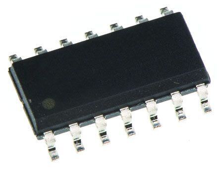
ICGOO电子元器件商城为您提供SN75189ADR由Texas Instruments设计生产,在icgoo商城现货销售,并且可以通过原厂、代理商等渠道进行代购。 SN75189ADR价格参考。Texas InstrumentsSN75189ADR封装/规格:接口 - 驱动器,接收器,收发器, 接收器 0/4 RS232 14-SOIC。您可以下载SN75189ADR参考资料、Datasheet数据手册功能说明书,资料中有SN75189ADR 详细功能的应用电路图电压和使用方法及教程。
| 参数 | 数值 |
| 产品目录 | 集成电路 (IC)半导体 |
| 描述 | IC QUAD LINE RECEIVER 14-SOICRS-232接口集成电路 Quad Line |
| 产品分类 | |
| 品牌 | Texas Instruments |
| 产品手册 | |
| 产品图片 |
|
| rohs | 符合RoHS无铅 / 符合限制有害物质指令(RoHS)规范要求 |
| 产品系列 | 接口 IC,RS-232接口集成电路,Texas Instruments SN75189ADR- |
| 数据手册 | |
| 产品型号 | SN75189ADR |
| 产品种类 | RS-232接口集成电路 |
| 供应商器件封装 | 14-SOIC |
| 其它名称 | 296-1277-2 |
| 功能 | Receiver |
| 包装 | 带卷 (TR) |
| 协议 | RS232 |
| 单位重量 | 129.400 mg |
| 双工 | - |
| 商标 | Texas Instruments |
| 安装类型 | 表面贴装 |
| 安装风格 | SMD/SMT |
| 封装 | Reel |
| 封装/外壳 | 14-SOIC(0.154",3.90mm 宽) |
| 封装/箱体 | SOIC-14 |
| 工作温度 | 0°C ~ 70°C |
| 工作温度范围 | 0 C to + 70 C |
| 工作电源电压 | 5 V |
| 工厂包装数量 | 2500 |
| 接收器滞后 | - |
| 接收机数量 | 4 Receiver |
| 数据速率 | - |
| 最大工作温度 | + 70 C |
| 最小工作温度 | 0 C |
| 标准包装 | 2,500 |
| 激励器数量 | 0 Driver |
| 电压-电源 | 4.5 V ~ 5.5 V |
| 电源电流 | 26 mA |
| 类型 | 接收器 |
| 系列 | SN75189A |
| 驱动器/接收器数 | 0/4 |


- 商务部:美国ITC正式对集成电路等产品启动337调查
- 曝三星4nm工艺存在良率问题 高通将骁龙8 Gen1或转产台积电
- 太阳诱电将投资9.5亿元在常州建新厂生产MLCC 预计2023年完工
- 英特尔发布欧洲新工厂建设计划 深化IDM 2.0 战略
- 台积电先进制程称霸业界 有大客户加持明年业绩稳了
- 达到5530亿美元!SIA预计今年全球半导体销售额将创下新高
- 英特尔拟将自动驾驶子公司Mobileye上市 估值或超500亿美元
- 三星加码芯片和SET,合并消费电子和移动部门,撤换高东真等 CEO
- 三星电子宣布重大人事变动 还合并消费电子和移动部门
- 海关总署:前11个月进口集成电路产品价值2.52万亿元 增长14.8%


PDF Datasheet 数据手册内容提取
MC1489, MC1489A, SN55189, SN55189A, SN75189, SN75189A QUADRUPLE LINE RECEIVERS SLLS095D – SEPTEMBER 1973 – REVISED OCTOBER 1998 (cid:1) Input Resistance...3 kW to 7 kW SN55189, SN55189A...J OR W PACKAGE (cid:1) Input Signal Range...±30 V MC1489D, M, NC,1 O48R9 NAS, S† NP7A5C1K89A,G SEN75189A (cid:1) Operate From Single 5-V Supply (TOP VIEW) (cid:1) Built-In Input Hysteresis (Double Thresholds) 1A 1 14 VCC (cid:1) 1CONT 2 13 4A Response Control that Provides: 1Y 3 12 4CONT Input Threshold Shifting Input Noise Filtering 2A 4 11 4Y (cid:1) 2CONT 5 10 3A Meet or Exceed the Requirements of 2Y 6 9 3CONT TIA/EIA-232-F and ITU Recommendation GND 7 8 3Y V.28 (cid:1) Fully Interchangeable With Motorola †The NS package is only available left-end taped and reeled. MC1489 and MC1489A For SN75189, order SN75189NSR. description SN55189, SN55189A...FK PACKAGE (TOP VIEW) These devices are monolithic low-power Schottky quadruple line receivers designed to satisfy the T N requirements of the standard interface between O C C A C CA data-terminal equipment and data-communica- 1 1 NV 4 tion equipment as defined by TIA/EIA-232-F. A separate response-control (CONT) terminal is 1Y 43 2 1 20 1918 4CONT provided for each receiver. A resistor or a resistor NC 5 17 NC and bias-voltage source can be connected 2A 6 16 4Y between this terminal and ground to shift the input NC 7 15 NC threshold levels. An external capacitor can be 2CONT 8 14 3A connected between this terminal and ground to 9 10 11 12 13 provide input noise filtering. Y D CY T The SN55189 and SN55189A are characterized 2 GN N3 ON for operation over the full military temperature C 3 range of –55°C to 125°C. The MC1489, NC – No internal connection MC1489A, SN75189, and SN75189A are characterized for operation from 0°C to 70°C. Please be aware that an important notice concerning availability, standard warranty, and use in critical applications of TexasInstruments semiconductor products and disclaimers thereto appears at the end of this data sheet. Motorola is a trademark of Motorola, Incorporated. PRODUCTION DATA information is current as of publication date. Copyright 1998, Texas Instruments Incorporated Products conform to specifications per the terms of Texas Instruments On products compliant to MIL-PRF-38535, all parameters are tested standard warranty. Production processing does not necessarily include unless otherwise noted. On all other products, production testing of all parameters. processing does not necessarily include testing of all parameters. POST OFFICE BOX 655303 • DALLAS, TEXAS 75265 1
MC1489, MC1489A, SN55189, SN55189A, SN75189, SN75189A QUADRUPLE LINE RECEIVERS SLLS095D – SEPTEMBER 1973 – REVISED OCTOBER 1998 logic symbol† 1 1A 3 1 CONT 2 THRS ADJ 1Y 4 2 CON2AT 5 6 2Y 3A 10 8 3Y 3 CONT 9 13 11 4A 4Y 12 4 CONT †This symbol is in accordance with ANSI/IEEE Std 91-1984 and IEC Publication 617-12. Pin numbers shown are for the D, J, N, NS, and W packages. logic diagram (positive logic) A Y Response Control schematic (each receiver) VCC 9 kW 5 kW 1.66 kW Output Y Response R1 Control 4 kW Input A 10 kW GND MC1489 MC1489A SN55189 SN55189A SN75189 SN75189A R1 8.4 kW 1.84 kW Resistor values shown are nominal. 2 POST OFFICE BOX 655303 • DALLAS, TEXAS 75265
MC1489, MC1489A, SN55189, SN55189A, SN75189, SN75189A QUADRUPLE LINE RECEIVERS SLLS095D – SEPTEMBER 1973 – REVISED OCTOBER 1998 absolute maximum ratings over operating free-air temperature (unless otherwise noted)† Supply voltage, V (see Note 1) . . . . . . . . . . . . . . . . . . . . . . . . . . . . . . . . . . . . . . . . . . . . . . . . . . . . . . . . . . . . 10 V CC Input voltage, V . . . . . . . . . . . . . . . . . . . . . . . . . . . . . . . . . . . . . . . . . . . . . . . . . . . . . . . . . . . . . . . . . . . . . . . . . . ±30 V I Output voltage, I . . . . . . . . . . . . . . . . . . . . . . . . . . . . . . . . . . . . . . . . . . . . . . . . . . . . . . . . . . . . . . . . . . . . . . . . 20 mA O Continuous total power dissipation . . . . . . . . . . . . . . . . . . . . . . . . . . . . . . . . . . . . . See Dissipation Rating Table Operating free-air temperature range, T : SN55189, SN55189A . . . . . . . . . . . . . . . . . . . . . . –55°C to 125°C A MC1489, MC1489A, SN75189, SN75189A . . . . . . 0°C to 70°C Storage temperature range, T . . . . . . . . . . . . . . . . . . . . . . . . . . . . . . . . . . . . . . . . . . . . . . . . . . . –65°C to 150°C stg Case temperature for 60 seconds, FK package . . . . . . . . . . . . . . . . . . . . . . . . . . . . . . . . . . . . . . . . . . . . . . 260°C Lead temperature 1,6 mm (1/16 inch) from case for 60 seconds: J or W package . . . . . . . . . . . . . . . . 300°C Lead temperature 1,6 mm (1/16 inch) from case for 10 seconds: D, N, or NS package . . . . . . . . . . . . 260°C †Stresses beyond those listed under “absolute maximum ratings” may cause permanent damage to the device. These are stress ratings only, and functional operation of the device at these or any other conditions beyond those indicated under “recommended operating conditions” is not implied. Exposure to absolute-maximum-rated conditions for extended periods may affect device reliability. NOTES: 1. All voltage values are with respect to the network ground terminal. DISSIPATION RATING TABLE TAA ≤ 25°C DERATING FACTOR TAA = 70°C TAA = 125°C PPAACCKKAAGGEE POWER RATING ABOVE TA = 25°C POWER RATING POWER RATING D 950 mW 7.6 mW/°C 608 mW N/A FK 1375 mW 11.0 mW/°C 880 mW 275 mW J‡ 1375 mW 11.0 mW/°C 880 mW 275 mW N 1150 mW 9.2 mW/°C 736 mW N/A NS 625 mW 4.0 mW/°C 445 mW N/A W 1000 mW 8.0 mW/°C 640 mW 200 mW ‡In the J package, SN55189 and SN55189A chips are either silver glass or alloy mounted. recommended operating conditions MIN NOM MAX UNIT Supply voltage, VCC 4.5 5 5.5 V Input voltage, VI –25 25 V High-level output current, IOH –0.5 mA Low-level output current, IOL 10 mA Operating free-air temperature, TA 0 70 °C POST OFFICE BOX 655303 • DALLAS, TEXAS 75265 3
MC1489, MC1489A, SN55189, SN55189A, SN75189, SN75189A QUADRUPLE LINE RECEIVERS SLLS095D – SEPTEMBER 1973 – REVISED OCTOBER 1998 electrical characteristics over operating free-air temperature range, V = 5 V ± 1% (unless CC otherwise noted) MC1489, MC1489A SN55189 TTEESSTT SSNN7755118899 PARAMETER FIGURE TEST CONDITIONS†† SN55189A SN75189A UNIT MIN TYP‡ MAX MIN TYP‡ MAX TA = 25°C 1 1.3 1.5 1 1.3 1.5 ’89 TA = 0°C to 70°C 0.9 1.6 Positive-ggoingg input TA = –55°C to 125°C 0.6 1.9 VVIITT+ 11 VV threshold voltage TA = 25°C 1.75 1.9 2.25 1.75 1.9 2.25 ’89A TA = 0°C to 70°C 1.55 2.25 TA = –55°C to 125°C 1.30 2.65 TA = 25°C 0.75 1.0 1.25 0.75 1.0 1.25 NNegattiive-goiing iinputt VIT– 1 ’89, ’89A TA = 0°C to 70°C 0.65 1.25 V tthhrreesshhoolldd vvoollttaaggee TA = –55°C to 125°C 0.35 1.6 Higgh-level VI = 0.75 V, IOH = –0.5 mA 2.6 4 5 2.6 4 5 VVOOHH 11 VV output voltage Input open, IOH = –0.5 mA 2.6 4 5 2.6 4 5 Low-level VVOOLL 11 VVII == 33 VV, IIOOLL == 1100 mmAA 00.22 00.4455 00.22 00.4455 VV output voltage Higgh-level VI = 25 V 3.6 8.3 3.6 8.3 IIIIHH 22 mmAA input current VI = 3 V 0.43 0.43 Low-level VI = –25 V –3.6 –8.3 –3.6 –8.3 IIIILL 22 mmAA input current VI = –3 V –0.43 –0.43 Short-circuit IIOOSS 33 –33 –33 mmAA output current ICC Supply current 2 VI = 5 V, Outputs open 20 26 20 26 mA †All characteristics are measured with the response-control terminal open. ‡All typical values are at VCC = 5 V, TA = 25°C. switching characteristics, V = 5 V, C = 15 pF, T = 25°C CC L A TEST PPAARRAAMMEETTEERR TTEESSTT CCOONNDDIITTIIOONNSS MMIINN TTYYPP MMAAXX UUNNIITT FIGURE tPLH Propagation delay time, low- to high-level output RL = 3.9 kW 25 85 nnss tPHL Propagation delay time, high- to low-level output RL = 390 W 25 50 44 tTLH Transition time, low- to high-level output RL = 3.9 kW 120 175 nnss tTHL Transition time, high- to low-level output RL = 390 W 10 20 4 POST OFFICE BOX 655303 • DALLAS, TEXAS 75265
MC1489, MC1489A, SN55189, SN55189A, SN75189, SN75189A QUADRUPLE LINE RECEIVERS SLLS095D – SEPTEMBER 1973 – REVISED OCTOBER 1998 PARAMETER MEASUREMENT INFORMATION† VCC VIT, V1 –IOH VOH Response Control IOL VOL Open RC RC Unless Otherwise CC Specified –VC +VC Figure 1. V , V , V , V IT+ IT– OH OL VCC ICC (see Note A) IIH VI Open IIL Response Control Open NOTE A: ICC is tested for all four receivers simultaneously. Figure 2. I , I , I IH IL CC VCC –IOS Response Control Open Figure 3. I OS †Arrows indicate actual direction of current flow. Current into a terminal is a positive value. POST OFFICE BOX 655303 • DALLAS, TEXAS 75265 5
MC1489, MC1489A, SN55189, SN55189A, SN75189, SN75189A QUADRUPLE LINE RECEIVERS SLLS095D – SEPTEMBER 1973 – REVISED OCTOBER 1998 PARAMETER MEASUREMENT INFORMATION VCC Output RL Pulse Generator (see Note A) See Note C Response CL = 15 pF Control (see Note B) Open TEST CIRCUIT ≤10 ns ≤10 ns 4 V 90% 90% Input 50% 50% 10% 10% 0 V tPHL tPLH VOH Output 90% 50% 50% 90% 10% 10% VOL tTHL tTLH VOLTAGE WAVEFORMS NOTES: A. The pulse generator has the following characteristics: ZO = 50 W , tw = 500 ns. B. CL includes probe and jig capacitances. C. All diodes are 1N3064 or equivalent. Figure 4. Test Circuit and Voltage Waveforms 6 POST OFFICE BOX 655303 • DALLAS, TEXAS 75265
MC1489, MC1489A, SN55189, SN55189A, SN75189, SN75189A QUADRUPLE LINE RECEIVERS SLLS095D – SEPTEMBER 1973 – REVISED OCTOBER 1998 TYPICAL CHARACTERISTICS SN65189, SN75189 OUTPUT VOLTAGE vs INPUT VOLTAGE ÁÁÁ ÁÁÁÁ ÁÁÁÁ ÁÁÁÁ 6 5 ÁÁVRCC ÁÁ== 55 VkÁÁW ÁÁRVÁÁCC ==ÁÁ 51 3V kÁÁW Î RÎC =Î ∞ Î ÁÁRVÁÁCC ==ÁÁ –115 kÁÁVW ÁÁÁÁÁÁÁTVÁÁÁÁÁAC C= =2ÁÁÁÁÁ5 5° CVÁÁÁÁÁ V See Figure 1 – ÁÁÁÁÁÁÁÁÁ e g 4 a olt V ÎÎÎÎÎÎ ÎÎÎÎ put 3 VIT– ÎVIÎT+ ÎÎVÎIT–Î VIT+ VIT– ÎÎVIT+ÎÎ VIT– VIT+ ut O 2 – O O VV 1 0 –3 –2 –1 0 1 2 3 4 5 VI – Input Voltage – V Figure 5 SN65189A, SN75189A OUTPUT VOLTAGE vs INPUT VOLTAGE 6 ÁÁÁÁ ÎÎÎÎ ÁÁÁÁÁÁÁÁÁ RC = 5 kW RC = ∞ RC = 11 kW VCC = 5 V ÁÁVC =Á 5 VÁ ÎÎÎÎ ÁVCÁ = –Á5 VÁÁÁTA Á= 25Á°C Á 5 V ÁÁSeeÁ FigÁure 1Á – e g 4 a olt V ut 3 p VIT– VIT+ VIT– VIT+ VIT– VIT+ ut O 2 – O O VV 1 0 –3 –2 –1 0 1 2 3 4 5 VI – Input Voltage – V Figure 6 POST OFFICE BOX 655303 • DALLAS, TEXAS 75265 7
MC1489, MC1489A, SN55189, SN55189A, SN75189, SN75189A QUADRUPLE LINE RECEIVERS SLLS095D – SEPTEMBER 1973 – REVISED OCTOBER 1998 TYPICAL CHARACTERISTICS† INPUT THRESHOLD VOLTAGE INPUT THRESHOLD VOLTAGE vs vs FREE-AIR TEMPERATURE SUPPLY VOLTAGE 2.4 2 2.2 1.8 Î’Î89AÎ VITÎ+ V – hold Voltage 11..862 ’89A VIT+ d Voltage – V 111...642 ÎÎÎ’8’899 ÎÎÎV VITIT+ÎÎΖ res 1.4 ’89 VIT+ hol 1 ÎÎÎ h s – Input T 1.21 ’89 VIT– nput Thre 00..86 ÎÎ’89AÎ VITΖ VIT 0.8 ’89A VIT– – IT 0.4 VI 0.6 0.2 0.4 0 –100 –75 –50 –25 0 25 50 75 100 125 150 2 3 4 5 6 7 8 9 10 TA – Free-Air Temperature – °C VCC – Supply Voltage – V Figure 7 Figure 8 SN75189 SN75189A NOISE REJECTION NOISE REJECTION 6 6 ÎÎÎÎ TVAC C= =25 5° CV ÎVTACÎ C= =25 Î5° CVÎ 5 ÎÎSeeÎ NotÎe AÎ 5 ÎSeÎe NoÎte AÎ ÎÁÎÁÎÁÎÁÎ ÎÎÎÎÎ CC = 300 pF 4 ÎÎÁÁÎÎCC ÁÁÎÎ= 30ÁÁÎÎ0 pFÁÁÎÎ 4 V V – ÎÁÎCC ÁÎ= 50ÁÎ0 pFÁÎ – ÁÎÁÎÁÎÁÎÁÎ de de ÁÎÁÎCC =ÁÎ 500ÁÎ pFÁÎ u 3 u 3 plit plit ÁÁÁÁ m m A A ÁCÁC = 1Á2 pFÁ 2 2 ÁÁÁÁ ÎÁÎÁÎÁÎÁÎ CC = 10 pF CC = 100 pF ÁÁÁÁÁÁÁÁ ÎÁÎÁÎÁÎÁÎ 1 CC = 100 pF 1 ÁÁÁÁ 0 0 10 40 100 400 1000 400010000 10 40 100 400 1000 4000 10000 tw – Pulse Duration – ns tw – Pulse Duration – ns NOTE A: Maximum amplitude of a positive-going pulse that, NOTE A: Maximum amplitude of a positive-going pulse that, starting from 0 V, will not cause a change in the starting from 0 V, will not cause a change in the output level. output level. Figure 9 Figure 10 †Data for free-air temperatures below 0°C and above 70°C are applicable to SN55189 and SN55189A circuits only. 8 POST OFFICE BOX 655303 • DALLAS, TEXAS 75265
MC1489, MC1489A, SN55189, SN55189A, SN75189, SN75189A QUADRUPLE LINE RECEIVERS SLLS095D – SEPTEMBER 1973 – REVISED OCTOBER 1998 TYPICAL CHARACTERISTICS INPUT CURRENT vs INPUT VOLTAGE 10 ÎÎÎÎÎ VCC = 5 V 8 ÁÎCoÁÎntroÁÎl OpÁÎen Î 6 ÎTAÎ = 25ΰC ÎÎ A 4 m – nt 2 e r ur 0 C ut p –2 n II – III –4 –6 –8 –10 –25 –20 –15 –10 –5 0 5 10 15 20 25 VI – Input Voltage – V Figure 11 POST OFFICE BOX 655303 • DALLAS, TEXAS 75265 9
PACKAGE OPTION ADDENDUM www.ti.com 26-Sep-2018 PACKAGING INFORMATION Orderable Device Status Package Type Package Pins Package Eco Plan Lead/Ball Finish MSL Peak Temp Op Temp (°C) Device Marking Samples (1) Drawing Qty (2) (6) (3) (4/5) 5962-86888022A ACTIVE LCCC FK 20 1 TBD POST-PLATE N / A for Pkg Type -55 to 125 5962- 86888022A SNJ55 189AFK 5962-8688802CA ACTIVE CDIP J 14 1 TBD A42 N / A for Pkg Type -55 to 125 5962-8688802CA SNJ55189AJ 5962-8688802DA ACTIVE CFP W 14 1 TBD A42 N / A for Pkg Type -55 to 125 5962-8688802DA SNJ55189AW MC1489AN ACTIVE PDIP N 14 25 Green (RoHS CU NIPDAU N / A for Pkg Type 0 to 70 MC1489AN & no Sb/Br) MC1489N ACTIVE PDIP N 14 25 Green (RoHS CU NIPDAU N / A for Pkg Type 0 to 70 MC1489N & no Sb/Br) MC1489NE4 ACTIVE PDIP N 14 25 Green (RoHS CU NIPDAU N / A for Pkg Type 0 to 70 MC1489N & no Sb/Br) SN55189AJ ACTIVE CDIP J 14 1 TBD A42 N / A for Pkg Type -55 to 125 SN55189AJ SN75189AD ACTIVE SOIC D 14 50 Green (RoHS CU NIPDAU Level-1-260C-UNLIM 0 to 70 SN75189A & no Sb/Br) SN75189ADR ACTIVE SOIC D 14 2500 Green (RoHS CU NIPDAU Level-1-260C-UNLIM 0 to 70 SN75189A & no Sb/Br) SN75189ADRG4 ACTIVE SOIC D 14 2500 Green (RoHS CU NIPDAU Level-1-260C-UNLIM 0 to 70 SN75189A & no Sb/Br) SN75189AN ACTIVE PDIP N 14 25 Green (RoHS CU NIPDAU N / A for Pkg Type 0 to 70 SN75189AN & no Sb/Br) SN75189ANSR ACTIVE SO NS 14 2000 Green (RoHS CU NIPDAU Level-1-260C-UNLIM 0 to 70 SN75189A & no Sb/Br) SN75189ANSRG4 ACTIVE SO NS 14 2000 Green (RoHS CU NIPDAU Level-1-260C-UNLIM 0 to 70 SN75189A & no Sb/Br) SN75189APWR ACTIVE TSSOP PW 14 2000 Green (RoHS CU NIPDAU Level-1-260C-UNLIM A189A & no Sb/Br) SN75189D ACTIVE SOIC D 14 50 Green (RoHS CU NIPDAU Level-1-260C-UNLIM 0 to 70 SN75189 & no Sb/Br) SN75189DR ACTIVE SOIC D 14 2500 Green (RoHS CU NIPDAU Level-1-260C-UNLIM 0 to 70 SN75189 & no Sb/Br) Addendum-Page 1
PACKAGE OPTION ADDENDUM www.ti.com 26-Sep-2018 Orderable Device Status Package Type Package Pins Package Eco Plan Lead/Ball Finish MSL Peak Temp Op Temp (°C) Device Marking Samples (1) Drawing Qty (2) (6) (3) (4/5) SN75189N ACTIVE PDIP N 14 25 Green (RoHS CU NIPDAU N / A for Pkg Type 0 to 70 SN75189N & no Sb/Br) SN75189NSR ACTIVE SO NS 14 2000 Green (RoHS CU NIPDAU Level-1-260C-UNLIM 0 to 70 SN75189 & no Sb/Br) SNJ55189AFK ACTIVE LCCC FK 20 1 TBD POST-PLATE N / A for Pkg Type -55 to 125 5962- 86888022A SNJ55 189AFK SNJ55189AJ ACTIVE CDIP J 14 1 TBD A42 N / A for Pkg Type -55 to 125 5962-8688802CA SNJ55189AJ SNJ55189AW ACTIVE CFP W 14 1 TBD A42 N / A for Pkg Type -55 to 125 5962-8688802DA SNJ55189AW (1) The marketing status values are defined as follows: ACTIVE: Product device recommended for new designs. LIFEBUY: TI has announced that the device will be discontinued, and a lifetime-buy period is in effect. NRND: Not recommended for new designs. Device is in production to support existing customers, but TI does not recommend using this part in a new design. PREVIEW: Device has been announced but is not in production. Samples may or may not be available. OBSOLETE: TI has discontinued the production of the device. (2) RoHS: TI defines "RoHS" to mean semiconductor products that are compliant with the current EU RoHS requirements for all 10 RoHS substances, including the requirement that RoHS substance do not exceed 0.1% by weight in homogeneous materials. Where designed to be soldered at high temperatures, "RoHS" products are suitable for use in specified lead-free processes. TI may reference these types of products as "Pb-Free". RoHS Exempt: TI defines "RoHS Exempt" to mean products that contain lead but are compliant with EU RoHS pursuant to a specific EU RoHS exemption. Green: TI defines "Green" to mean the content of Chlorine (Cl) and Bromine (Br) based flame retardants meet JS709B low halogen requirements of <=1000ppm threshold. Antimony trioxide based flame retardants must also meet the <=1000ppm threshold requirement. (3) MSL, Peak Temp. - The Moisture Sensitivity Level rating according to the JEDEC industry standard classifications, and peak solder temperature. (4) There may be additional marking, which relates to the logo, the lot trace code information, or the environmental category on the device. (5) Multiple Device Markings will be inside parentheses. Only one Device Marking contained in parentheses and separated by a "~" will appear on a device. If a line is indented then it is a continuation of the previous line and the two combined represent the entire Device Marking for that device. (6) Lead/Ball Finish - Orderable Devices may have multiple material finish options. Finish options are separated by a vertical ruled line. Lead/Ball Finish values may wrap to two lines if the finish value exceeds the maximum column width. Addendum-Page 2
PACKAGE OPTION ADDENDUM www.ti.com 26-Sep-2018 Important Information and Disclaimer:The information provided on this page represents TI's knowledge and belief as of the date that it is provided. TI bases its knowledge and belief on information provided by third parties, and makes no representation or warranty as to the accuracy of such information. Efforts are underway to better integrate information from third parties. TI has taken and continues to take reasonable steps to provide representative and accurate information but may not have conducted destructive testing or chemical analysis on incoming materials and chemicals. TI and TI suppliers consider certain information to be proprietary, and thus CAS numbers and other limited information may not be available for release. In no event shall TI's liability arising out of such information exceed the total purchase price of the TI part(s) at issue in this document sold by TI to Customer on an annual basis. OTHER QUALIFIED VERSIONS OF SN55189A, SN75189A : •Catalog: SN75189A •Military: SN55189A NOTE: Qualified Version Definitions: •Catalog - TI's standard catalog product •Military - QML certified for Military and Defense Applications Addendum-Page 3
PACKAGE MATERIALS INFORMATION www.ti.com 27-Sep-2018 TAPE AND REEL INFORMATION *Alldimensionsarenominal Device Package Package Pins SPQ Reel Reel A0 B0 K0 P1 W Pin1 Type Drawing Diameter Width (mm) (mm) (mm) (mm) (mm) Quadrant (mm) W1(mm) SN75189ADR SOIC D 14 2500 330.0 16.4 6.5 9.0 2.1 8.0 16.0 Q1 SN75189ADR SOIC D 14 2500 330.0 16.4 6.5 9.0 2.1 8.0 16.0 Q1 SN75189APWR TSSOP PW 14 2000 330.0 12.4 6.9 5.6 1.6 8.0 12.0 Q1 SN75189DR SOIC D 14 2500 330.0 16.4 6.5 9.0 2.1 8.0 16.0 Q1 SN75189NSR SO NS 14 2000 330.0 16.4 8.2 10.5 2.5 12.0 16.0 Q1 PackMaterials-Page1
PACKAGE MATERIALS INFORMATION www.ti.com 27-Sep-2018 *Alldimensionsarenominal Device PackageType PackageDrawing Pins SPQ Length(mm) Width(mm) Height(mm) SN75189ADR SOIC D 14 2500 367.0 367.0 38.0 SN75189ADR SOIC D 14 2500 333.2 345.9 28.6 SN75189APWR TSSOP PW 14 2000 367.0 367.0 35.0 SN75189DR SOIC D 14 2500 367.0 367.0 38.0 SN75189NSR SO NS 14 2000 367.0 367.0 38.0 PackMaterials-Page2
None
PACKAGE OUTLINE J0014A CDIP - 5.08 mm max height SCALE 0.900 CERAMIC DUAL IN LINE PACKAGE PIN 1 ID A 4X .005 MIN (OPTIONAL) [0.13] .015-.060 TYP [0.38-1.52] 1 14 12X .100 [2.54] 14X .014-.026 14X .045-.065 [0.36-0.66] [1.15-1.65] .010 [0.25] C A B .754-.785 [19.15-19.94] 7 8 B .245-.283 .2 MAX TYP .13 MIN TYP [6.22-7.19] [5.08] [3.3] SEATING PLANE C .308-.314 [7.83-7.97] AT GAGE PLANE .015 GAGE PLANE [0.38] 0 -15 14X .008-.014 TYP [0.2-0.36] 4214771/A 05/2017 NOTES: 1. All controlling linear dimensions are in inches. Dimensions in brackets are in millimeters. Any dimension in brackets or parenthesis are for reference only. Dimensioning and tolerancing per ASME Y14.5M. 2. This drawing is subject to change without notice. 3. This package is hermitically sealed with a ceramic lid using glass frit. 4. Index point is provided on cap for terminal identification only and on press ceramic glass frit seal only. 5. Falls within MIL-STD-1835 and GDIP1-T14. www.ti.com
EXAMPLE BOARD LAYOUT J0014A CDIP - 5.08 mm max height CERAMIC DUAL IN LINE PACKAGE (.300 ) TYP [7.62] SEE DETAIL B SEE DETAIL A 1 14 12X (.100 ) [2.54] SYMM 14X ( .039) [1] 7 8 SYMM LAND PATTERN EXAMPLE NON-SOLDER MASK DEFINED SCALE: 5X .002 MAX (.063) [0.05] [1.6] METAL ALL AROUND ( .063) SOLDER MASK [1.6] OPENING METAL .002 MAX SOLDER MASK (R.002 ) TYP [0.05] OPENING [0.05] ALL AROUND DETAIL A DETAIL B SCALE: 15X 13X, SCALE: 15X 4214771/A 05/2017 www.ti.com
None
None
None
None
None
None
None
None
IMPORTANTNOTICEANDDISCLAIMER TIPROVIDESTECHNICALANDRELIABILITYDATA(INCLUDINGDATASHEETS),DESIGNRESOURCES(INCLUDINGREFERENCE DESIGNS),APPLICATIONOROTHERDESIGNADVICE,WEBTOOLS,SAFETYINFORMATION,ANDOTHERRESOURCES“ASIS” ANDWITHALLFAULTS,ANDDISCLAIMSALLWARRANTIES,EXPRESSANDIMPLIED,INCLUDINGWITHOUTLIMITATIONANY IMPLIEDWARRANTIESOFMERCHANTABILITY,FITNESSFORAPARTICULARPURPOSEORNON-INFRINGEMENTOFTHIRD PARTYINTELLECTUALPROPERTYRIGHTS. TheseresourcesareintendedforskilleddevelopersdesigningwithTIproducts.Youaresolelyresponsiblefor(1)selectingtheappropriate TIproductsforyourapplication,(2)designing,validatingandtestingyourapplication,and(3)ensuringyourapplicationmeetsapplicable standards,andanyothersafety,security,orotherrequirements.Theseresourcesaresubjecttochangewithoutnotice.TIgrantsyou permissiontousetheseresourcesonlyfordevelopmentofanapplicationthatusestheTIproductsdescribedintheresource.Other reproductionanddisplayoftheseresourcesisprohibited.NolicenseisgrantedtoanyotherTIintellectualpropertyrightortoanythird partyintellectualpropertyright.TIdisclaimsresponsibilityfor,andyouwillfullyindemnifyTIanditsrepresentativesagainst,anyclaims, damages,costs,losses,andliabilitiesarisingoutofyouruseoftheseresources. TI’sproductsareprovidedsubjecttoTI’sTermsofSale(www.ti.com/legal/termsofsale.html)orotherapplicabletermsavailableeitheron ti.comorprovidedinconjunctionwithsuchTIproducts.TI’sprovisionoftheseresourcesdoesnotexpandorotherwisealterTI’sapplicable warrantiesorwarrantydisclaimersforTIproducts. MailingAddress:TexasInstruments,PostOfficeBox655303,Dallas,Texas75265 Copyright©2018,TexasInstrumentsIncorporated