ICGOO在线商城 > 集成电路(IC) > 逻辑 - 缓冲器,驱动器,接收器,收发器 > SN74LVC3G34DCUT
 Datasheet下载
- 型号: SN74LVC3G34DCUT
- 制造商: Texas Instruments
- 库位|库存: xxxx|xxxx
- 要求:
| 数量阶梯 | 香港交货 | 国内含税 |
| +xxxx | $xxxx | ¥xxxx |
查看当月历史价格
查看今年历史价格
SN74LVC3G34DCUT产品简介:
ICGOO电子元器件商城为您提供SN74LVC3G34DCUT由Texas Instruments设计生产,在icgoo商城现货销售,并且可以通过原厂、代理商等渠道进行代购。 SN74LVC3G34DCUT价格参考¥2.18-¥5.39。Texas InstrumentsSN74LVC3G34DCUT封装/规格:逻辑 - 缓冲器,驱动器,接收器,收发器, Buffer, Non-Inverting 3 Element 1 Bit per Element Push-Pull Output US8。您可以下载SN74LVC3G34DCUT参考资料、Datasheet数据手册功能说明书,资料中有SN74LVC3G34DCUT 详细功能的应用电路图电压和使用方法及教程。
| 参数 | 数值 |
| 产品目录 | 集成电路 (IC)半导体 |
| 描述 | IC BUFFER TRPL NON-INV US8缓冲器和线路驱动器 TRIPLE BUFFER GATE |
| 产品分类 | |
| 品牌 | Texas Instruments |
| 产品手册 | http://www.ti.com/lit/gpn/sn74lvc3g34 |
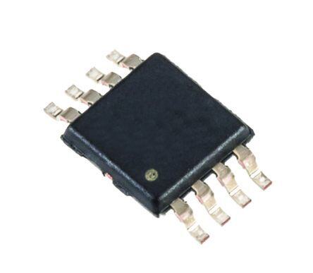
| 产品图片 |
|
| rohs | 符合RoHS无铅 / 符合限制有害物质指令(RoHS)规范要求 |
| 产品系列 | 逻辑集成电路,缓冲器和线路驱动器,Texas Instruments SN74LVC3G34DCUT74LVC |
| 数据手册 | |
| 产品型号 | SN74LVC3G34DCUT |
| 产品种类 | 缓冲器和线路驱动器 |
| 传播延迟时间 | 4.1 ns at 3.3 V, 3.2 ns at 5 V |
| 低电平输出电流 | 32 mA |
| 供应商器件封装 | US8 |
| 元件数 | 3 |
| 其它名称 | 296-32335-6 |
| 包装 | Digi-Reel® |
| 单位重量 | 9.600 mg |
| 商标 | Texas Instruments |
| 安装类型 | 表面贴装 |
| 安装风格 | SMD/SMT |
| 封装 | Reel |
| 封装/外壳 | 8-VFSOP(0.091",2.30mm 宽) |
| 封装/箱体 | VSSOP-8 |
| 工作温度 | -40°C ~ 125°C |
| 工厂包装数量 | 250 |
| 最大工作温度 | + 85 C |
| 最小工作温度 | - 40 C |
| 极性 | Non-Inverting |
| 标准包装 | 1 |
| 每元件位数 | 1 |
| 每芯片的通道数量 | 3 |
| 电压-电源 | 1.65 V ~ 5.5 V |
| 电流-输出高,低 | 32mA,32mA |
| 电源电压-最大 | 5.5 V |
| 电源电压-最小 | 1.65 V |
| 系列 | SN74LVC3G34 |
| 输入线路数量 | 3 |
| 输出线路数量 | 3 |
| 逻辑类型 | 缓冲器/线路驱动器,非反相 |
| 逻辑系列 | LVC |
| 配用 | /product-detail/zh/SN74LVC3G34DCUR/296-13286-2-ND/484593 |
| 高电平输出电流 | - 32 mA |


- 商务部:美国ITC正式对集成电路等产品启动337调查
- 曝三星4nm工艺存在良率问题 高通将骁龙8 Gen1或转产台积电
- 太阳诱电将投资9.5亿元在常州建新厂生产MLCC 预计2023年完工
- 英特尔发布欧洲新工厂建设计划 深化IDM 2.0 战略
- 台积电先进制程称霸业界 有大客户加持明年业绩稳了
- 达到5530亿美元!SIA预计今年全球半导体销售额将创下新高
- 英特尔拟将自动驾驶子公司Mobileye上市 估值或超500亿美元
- 三星加码芯片和SET,合并消费电子和移动部门,撤换高东真等 CEO
- 三星电子宣布重大人事变动 还合并消费电子和移动部门
- 海关总署:前11个月进口集成电路产品价值2.52万亿元 增长14.8%


PDF Datasheet 数据手册内容提取
Product Sample & Technical Tools & Support & Folder Buy Documents Software Community SN74LVC3G34 SCES366L–AUGUST2001–REVISEDOCTOBER2015 SN74LVC3G34 Triple Buffer Gate 1 Features 3 Description • AvailableintheTexasInstruments The SN74LVC3G34 device is a triple buffer gate 1 designed for 1.65-V to 5.5-V V operation. The NanoFree™Package CC SN74LVC3G34 device performs the Boolean function • Supports5.5-VV Operation CC Y=Ainpositivelogic. • InputsAcceptVoltagesto5.5V NanoFree package technology is a major • Maxt of4.1nsat3.3V pd breakthrough in IC packaging concepts, using the die • LowPowerConsumption,10-µAMaximumI asthepackage. CC • ±24-mAOutputDriveat3.3V This device is fully specified for partial-power-down • TypicalV (OutputGroundBounce) applications using I . The I circuitry disables the OLP off off <0.8VatV =3.3V,T =25°C outputs, preventing damaging current backflow CC A throughthedevicewhenitispowereddown. • TypicalV (OutputV Undershoot) OHV OH >2VatV =3.3V,T =25°C CC A DeviceInformation(1) • I SupportsLiveInsertion,Partial-Power-Down off PARTNUMBER PACKAGE BODYSIZE(NOM) Mode,andBack-DriveProtection SN74LVC3G34DCT SM8(8) 2.95mm×2.80mm • CanBeUsedasaDownTranslatortoTranslate SN74LVC3G34DCU VSSOP(8) 2.30mm×2.00mm InputsFromaMaximumof5.5VDowntotheV CC SN74LVC3G34YZP DSBGA(8) 1.91mm×0.91mm Level (1) For all available packages, see the orderable addendum at • Latch-UpPerformanceExceeds100mAPer theendofthedatasheet. JESD78,ClassII • ESDProtectionExceedsJESD22 SimplifiedSchematic – 2000-VHumanBodyModel(A114-A) 1 7 – 200-VMachineModel(A115-A) 1A 1Y – 1000-VCharged-DeviceModel(C101) 2 Applications 3 5 2A 2Y • AVReceivers • AudioDocks:Portable • Blu-rayPlayersandHomeTheaters 6 2 • DVDRecordersandPlayers 3A 3Y • EmbeddedPCs • MP3PlayersandRecorders(PortableAudio) • PersonalDigitalAssistant(PDA) • Power:Telecom/ServerAC/DCSupply:Single Controller:AnalogandDigital • Solid-StateDrive(SSD):ClientandEnterprise • TV:LCD/DigitalandHigh-Definition(HDTV) • Tablets:Enterprise • VideoAnalytics:Servers • WirelessHeadsets,Keyboards,andMice 1 An IMPORTANT NOTICE at the end of this data sheet addresses availability, warranty, changes, use in safety-critical applications, intellectualpropertymattersandotherimportantdisclaimers.PRODUCTIONDATA.
SN74LVC3G34 SCES366L–AUGUST2001–REVISEDOCTOBER2015 www.ti.com Table of Contents 1 Features.................................................................. 1 8.2 FunctionalBlockDiagram.........................................8 2 Applications........................................................... 1 8.3 FeatureDescription...................................................8 3 Description............................................................. 1 8.4 DeviceFunctionalModes..........................................8 4 RevisionHistory..................................................... 2 9 ApplicationandImplementation.......................... 9 9.1 ApplicationInformation..............................................9 5 PinConfigurationandFunctions......................... 3 9.2 TypicalApplication ...................................................9 6 Specifications......................................................... 3 10 PowerSupplyRecommendations..................... 10 6.1 AbsoluteMaximumRatings .....................................3 11 Layout................................................................... 10 6.2 ESDRatings..............................................................4 6.3 RecommendedOperatingConditions......................4 11.1 LayoutGuidelines.................................................10 6.4 ThermalInformation..................................................4 11.2 LayoutExample....................................................10 6.5 ElectricalCharacteristics..........................................5 12 DeviceandDocumentationSupport................. 11 6.6 SwitchingCharacteristics .........................................5 12.1 DocumentationSupport........................................11 6.7 OperatingCharacteristics..........................................5 12.2 CommunityResources..........................................11 6.8 TypicalCharacteristics..............................................6 12.3 Trademarks...........................................................11 7 ParameterMeasurementInformation..................7 12.4 ElectrostaticDischargeCaution............................11 12.5 Glossary................................................................11 8 DetailedDescription.............................................. 8 13 Mechanical,Packaging,andOrderable 8.1 Overview...................................................................8 Information........................................................... 11 4 Revision History NOTE:Pagenumbersforpreviousrevisionsmaydifferfrompagenumbersinthecurrentversion. ChangesfromRevisionJ(Feburary2007)toRevisionK Page • UpdateddocumenttonewTIdatasheetformat.................................................................................................................... 1 • RemovedOrderingInformationtable..................................................................................................................................... 1 • UpdatedFeaturessection...................................................................................................................................................... 1 • Updatedoperatingtemperaturerange................................................................................................................................... 4 ChangesfromRevisionK(November2013)toRevisionL Page • AddedApplications,DeviceInformationtable,PinConfigurationandFunctionssection,ESDRatingstable,Thermal Informationtable,TypicalCharacteristicssection,FeatureDescriptionsection,DeviceFunctionalModes, ApplicationandImplementationsection,PowerSupplyRecommendationssection,Layoutsection,Deviceand DocumentationSupportsection,andMechanical,Packaging,andOrderableInformationsection ..................................... 1 • DeletedpartnumberfromSwitchingCharacteristicstableheaders...................................................................................... 5 2 SubmitDocumentationFeedback Copyright©2001–2015,TexasInstrumentsIncorporated ProductFolderLinks:SN74LVC3G34
SN74LVC3G34 www.ti.com SCES366L–AUGUST2001–REVISEDOCTOBER2015 5 Pin Configuration and Functions DCTPackage 8-PinSM8 DCUPackage TopView 8-PinVSSOP TopView 1A 1 8 VCC 1A 1 8 VCC 3Y 2 7 1Y 3Y 2 7 1Y 2A 3 6 3A 2A 3 6 3A GND 4 5 2Y GND 4 5 2Y YZPPackage 8-PinDSBGA BottomView GND 45 2Y 2A 36 3A 3Y 27 1Y 1A 18 VCC PinFunctions(1) PIN I/O DESCRIPTION NAME NO. 1A 1 I BufferInput1 1Y 7 O BufferOutput1 2A 3 I BufferInput2 2Y 5 O BufferOutput2 3A 6 I BufferInput3 3Y 2 O BufferOutput3 GND 4 — Groundpin VCC 8 — Powerpin (1) Seemechanicaldrawingsfordimensions 6 Specifications 6.1 Absolute Maximum Ratings overoperatingfree-airtemperaturerange(unlessotherwisenoted)(1) MIN MAX UNIT V Supplyvoltage –0.5 6.5 V CC V Inputvoltage(2) –0.5 6.5 V I V Voltageappliedtoanyoutputinthehigh-impedanceorpower-offstate(2) –0.5 6.5 V O V Voltageappliedtoanyoutputinthehighorlowstate(2)(3) –0.5 V +0.5 V O CC I Inputclampcurrent V <0 –50 mA IK I I Outputclampcurrent V <0 –50 mA OK O I Continuousoutputcurrent ±50 mA O ContinuouscurrentthroughV orGND ±100 mA CC T Junctiontemperature 150 °C J T Storagetemperature -65 150 °C stg (1) StressesbeyondthoselistedunderAbsoluteMaximumRatingsmaycausepermanentdamagetothedevice.Thesearestressratings only,andfunctionaloperationofthedeviceattheseoranyotherconditionsbeyondthoseindicatedunderRecommendedOperating Conditionsisnotimplied.Exposuretoabsolute-maximum-ratedconditionsforextendedperiodsmayaffectdevicereliability. (2) Theinputnegative-voltageandoutputvoltageratingsmaybeexceedediftheinputandoutputclamp-currentratingsareobserved. (3) ThevalueofV isprovidedintheRecommendedOperatingConditionstable. CC Copyright©2001–2015,TexasInstrumentsIncorporated SubmitDocumentationFeedback 3 ProductFolderLinks:SN74LVC3G34
SN74LVC3G34 SCES366L–AUGUST2001–REVISEDOCTOBER2015 www.ti.com 6.2 ESD Ratings VALUE UNIT Humanbodymodel(HBM),perANSI/ESDA/JEDECJS-001,allpins(1) 2500 Electrostatic V(ESD) discharge Cpihnasr(g2)ed-devicemodel(CDM),perJEDECspecificationJESD22-C101,all 1500 V (1) JEDECdocumentJEP155statesthat500-VHBMallowssafemanufacturingwithastandardESDcontrolprocess. (2) JEDECdocumentJEP157statesthat250-VCDMallowssafemanufacturingwithastandardESDcontrolprocess. 6.3 Recommended Operating Conditions(1) MIN MAX UNIT Operating 1.65 5.5 V Supplyvoltage V CC Dataretentiononly 1.5 V =1.65Vto1.95V 0.65×V CC CC V =2.3Vto2.7V 1.7 CC V High-levelinputvoltage V IH V =3Vto3.6V 2 CC V =4.5Vto5.5V 0.7×V CC CC V =1.65Vto1.95V 0.35×V CC CC V =2.3Vto2.7V 0.7 CC V Low-levelinputvoltage V IL V =3Vto3.6V 0.8 CC V =4.5Vto5.5V 0.3×V CC CC V Inputvoltage 0 5.5 V I V Outputvoltage 0 V V O CC V =1.65V –4 CC V =2.3V –8 CC I High-leveloutputcurrent –16 mA OH V =3V CC –24 V =4.5V –32 CC V =1.65V 4 CC V =2.3V 8 CC I Low-leveloutputcurrent 16 mA OL V =3V CC 24 V =4.5V 32 CC V =1.8V±0.15V,2.5V±0.2V 20 CC Δt/Δv Inputtransitionriseorfallrate V =3.3V±0.3V 10 ns/V CC V =5V±0.5V 5 CC DCT,DCUPackage –40 125 T Operatingfree-airtemperature °C A YZPPackage -40 85 (1) AllunusedinputsofthedevicemustbeheldatV orGNDtoensureproperdeviceoperation.RefertotheTIapplicationreport, CC ImplicationsofSloworFloatingCMOSInputs,SCBA004. 6.4 Thermal Information SN74LVC3G34 THERMALMETRIC(1) DCT(SM8) DCU(VSSOP) YZP(DSBGA) UNIT 8PINS 8PINS 8PINS R Junction-to-ambientthermalresistance 220 227 140 °C/W θJA (1) Formoreinformationabouttraditionalandnewthermalmetrics,seetheSemiconductorandICPackageThermalMetricsapplication report,SPRA953. 4 SubmitDocumentationFeedback Copyright©2001–2015,TexasInstrumentsIncorporated ProductFolderLinks:SN74LVC3G34
SN74LVC3G34 www.ti.com SCES366L–AUGUST2001–REVISEDOCTOBER2015 6.5 Electrical Characteristics overrecommendedoperatingfree-airtemperaturerange(unlessotherwisenoted) PARAMETER TESTCONDITIONS VCC MIN TYP(1) MAX UNIT IOH=–100µA 1.65Vto5.5V VCC–0.1 IOH=–4mA 1.65V 1.2 IOH=–8mA 2.3V 1.9 VOH V IOH=–16mA 2.4 3V IOH=–24mA 2.3 IOH=–32mA 4.5V 3.8 IOL=100µA 1.65Vto5.5V 0.1 IOL=4mA 1.65V 0.45 IOL=8mA 2.3V 0.3 IOL=16mA 3V 0.4 TA=–40°Cto 0.55 VOL IOL=24mA 85°C 3V V TA=–40°Cto 0.75 125°C TA=–40°Cto 0.55 85°C IOL=32mA 4.5V TA=–40°Cto 0.75 125°C II Ainputs VI=5.5VorGND 0to5.5V ±5 µA Ioff VIorVO=5.5V 0 ±10 µA ICC VI=5.5VorGND, IO=0 1.65Vto5.5V 10 µA ΔICC OOntheerinipnuptuatstaVtCVCC–C0o.r6GVN,D 3Vto5.5V 500 µA CI VI=VCCorGND T85A°=C–40°Cto 3.3V 3.5 pF (1) AlltypicalvaluesareatV =3.3V,T =25°C. CC A 6.6 Switching Characteristics overrecommendedoperatingfree-airtemperaturerange(unlessotherwisenoted)(seeFigure2) FROM TO OPERATINGFREE-AIR PARAMETER (INPUT) (OUTPUT) TEMPERATURE(TA) VCC MIN MAX UNIT VCC=1.8V±0.15V 3.2 7.9 VCC=2.5V±0.2V 1.5 4.4 tpd A Y –40°Cto85°C ns VCC=3.3V±0.3V 1.4 4.1 VCC=5V±0.5V 1.1 3.2 VCC=1.8V±0.15V 3.2 8.9 VCC=2.5V±0.2V 1.5 5.4 tpd A Y –40°Cto125°C ns VCC=3.3V±0.3V 1.4 5.1 VCC=5V±0.5V 1.1 3.8 6.7 Operating Characteristics T =25°C A PARAMETER TESTCONDITIONS V TYP UNIT CC V =1.8V 19 CC V =2.5V 19 CC C Powerdissipationcapacitance f=10MHz pF pd V =3.3V 19 CC V =5V 21 CC Copyright©2001–2015,TexasInstrumentsIncorporated SubmitDocumentationFeedback 5 ProductFolderLinks:SN74LVC3G34
SN74LVC3G34 SCES366L–AUGUST2001–REVISEDOCTOBER2015 www.ti.com 6.8 Typical Characteristics 2.5 TPD 2 s 1.5 n D - P T 1 0.5 0 -100 -50 0 50 100 150 Temperature - °C D001 Figure1.TPDAcrossTemperatureat3.3-VV CC 6 SubmitDocumentationFeedback Copyright©2001–2015,TexasInstrumentsIncorporated ProductFolderLinks:SN74LVC3G34
SN74LVC3G34 www.ti.com SCES366L–AUGUST2001–REVISEDOCTOBER2015 7 Parameter Measurement Information V LOAD R S1 Open From Output L TEST S1 Under Test GND t /t Open C PLH PHL (see NoteA)L RL tPLZ/tPZL VLOAD t /t GND PHZ PZH LOAD CIRCUIT INPUTS V V V C R V CC V t/t M LOAD L L D I r f 1.8 V±0.15 V V £2 ns V /2 2 ×V 30 pF 1 kW 0.15 V CC CC CC 2.5 V±0.2 V V £2 ns V /2 2 ×V 30 pF 500W 0.15 V CC CC CC 3.3 V±0.3 V 3 V £2.5 ns 1.5 V 6 V 50 pF 500W 0.3 V 5 V±0.5 V V £2.5 ns V /2 2 ×V 50 pF 500W 0.3 V CC CC CC V I Timing Input V M 0 V t W VI tsu th V Input V V I M M Data Input V V M M 0 V 0 V VOLTAGE WAVEFORMS VOLTAGE WAVEFORMS PULSE DURATION SETUPAND HOLD TIMES Input VM VM VI COounttpruotl VM VM VI 0 V 0 V t t t t PLH PHL PZL PLZ V Output V /2 Output VM VM OH WSav1e afot rVm 1 VM V + V LOAD VOL (see NoteL OBAD) OL D VOL t t PHL PLH t t PZH PHZ Output VM VM VOH WSa1v eaOfto uGrtmpNu D2t VM VOH–VD VOH VOL (see Note B) »0 V VOLTAGE WAVEFORMS VOLTAGE WAVEFORMS PROPAGATION DELAYTIMES ENABLEAND DISABLE TIMES INVERTINGAND NONINVERTING OUTPUTS LOW-AND HIGH-LEVELENABLING NOTES: A. C includes probe and jig capacitance. L B. Waveform 1 is for an output with internal conditions such that the output is low, except when disabled by the output control. Waveform 2 is for an output with internal conditions such that the output is high, except when disabled by the output control. C. All input pulses are supplied by generators having the following characteristics: PRR£10 MHz, Z = 50W. O D. The outputs are measured one at a time, with one transition per measurement. E. t and t are the same as t . PLZ PHZ dis F. t and t are the same as t . PZL PZH en G.t and t are the same as t . PLH PHL pd H. All parameters and waveforms are not applicable to all devices. Figure2. LoadCircuitandVoltageWaveforms Copyright©2001–2015,TexasInstrumentsIncorporated SubmitDocumentationFeedback 7 ProductFolderLinks:SN74LVC3G34
SN74LVC3G34 SCES366L–AUGUST2001–REVISEDOCTOBER2015 www.ti.com 8 Detailed Description 8.1 Overview The SN74LVC3G34 device contains three buffer gates that each perform the Boolean function Y = A. This device is fully specified for partial-power-down applications using I . The I circuitry disables the outputs, off off preventingdamagingcurrentbackflowthroughthedevicewhenitispowereddown. 8.2 Functional Block Diagram 1 7 1A 1Y 3 5 2A 2Y 6 2 3A 3Y 8.3 Feature Description The SN74LVC3G34 device has a wider operating voltage range, operating from 1.65 V to 5.5 V, and allows downvoltagetranslation.TheSN74LVC3G34I featureallowsvoltagesontheinputsandoutputswhenV is off CC 0V. 8.4 Device Functional Modes Table1liststhefunctionalmodesoftheSN74LVC3G34. Table1.FunctionTable INPUT OUTPUT A Y H H L L 8 SubmitDocumentationFeedback Copyright©2001–2015,TexasInstrumentsIncorporated ProductFolderLinks:SN74LVC3G34
SN74LVC3G34 www.ti.com SCES366L–AUGUST2001–REVISEDOCTOBER2015 9 Application and Implementation 9.1 Application Information The SN74LVC3G34 is a high-drive CMOS device that can be used as a buffer with a high output drive, such as an LED application. It can produce 24 mA of drive current at 3.3 V, making it ideal for driving multiple outputs and good for high-speed applications up to 100 MHz. The inputs are 5.5-V tolerant, allowing it to translate down toV . CC 9.2 Typical Application Buffer Function Basic LED Driver VCC VCC Microcontroller or Microcontroller or Microcontroller or SN74LVC3G34 SN74LVC3G34 Logic Logic Logic 9.2.1 DesignRequirements ThisdeviceusesCMOStechnologyandhasbalancedoutputdrive.Takecaretoavoidbuscontentionbecauseit can drive currents that would exceed maximum limits. The high drive will also create fast edges into light loads soroutingandloadconditionsmustbeconsideredtopreventringing. 9.2.2 DetailedDesignProcedure 1. RecommendedInputConditions – Risetimeandfalltimespecs.See(Δt/ΔV)intheRecommendedOperatingConditionstable. – Specifiedhighandlowlevels.See(V andV )intheRecommendedOperatingConditions table. IH IL – Inputs are overvoltage tolerant allowing them to go as high as (VI max) in the Recommended Operating ConditionstableatanyvalidV . CC 2. RecommendedOutputConditions – Loadcurrentsmustnotexceed(I max)peroutputandmustnotexceed(ContinuouscurrentthroughV O CC or GND) total current for the part. These limits are located in the Recommended Operating Conditions table. – OutputsmustnotbepulledaboveV undernormaloperatingconditions. CC Copyright©2001–2015,TexasInstrumentsIncorporated SubmitDocumentationFeedback 9 ProductFolderLinks:SN74LVC3G34
SN74LVC3G34 SCES366L–AUGUST2001–REVISEDOCTOBER2015 www.ti.com Typical Application (continued) 9.2.3 ApplicationCurve 5 TPD 4 s 3 n D - P T 2 1 0 0 1 2 3 4 5 6 Vcc - V D002 Figure3.TPDAcrossV at25°C CC 10 Power Supply Recommendations The power supply can be any voltage between the minimum and maximum supply voltage rating located in the RecommendedOperatingConditionstable. EachV pinmusthaveagoodbypasscapacitortopreventpowerdisturbance.Fordeviceswithasinglesupply, CC a 0.1-μF capacitor is recommended and if there are multiple V pins then a 0.01-μF or 0.022-μF capacitor is CC recommended for each power pin. It is ok to parallel multiple bypass caps to reject different frequencies of noise. 0.1-μF and 1-μF capacitors are commonly used in parallel. The bypass capacitor must be installed as close to thepowerpinaspossibleforbestresults. 11 Layout 11.1 Layout Guidelines When using multiple bit logic devices inputs must not ever float. In many cases, functions or parts of functions of digital logic devices are unused; for example, when only two inputs of a triple-input AND gate are used or only 3 of the 4 buffer gates are used. Such input pins must not be left unconnected because the undefined voltages at the outside connections result in undefined operational states. Specified below are the rules that must be observed under all circumstances. All unused inputs of digital logic devices must be connected to a high or low biastopreventthemfromfloating.Thelogiclevelthatmustbeappliedtoanyparticularunusedinputdependson the function of the device. Generally they will be tied to GND or V whichever make more sense or is more CC convenient. 11.2 Layout Example VCC Input Unused Input Output Unused Input Output Input 10 SubmitDocumentationFeedback Copyright©2001–2015,TexasInstrumentsIncorporated ProductFolderLinks:SN74LVC3G34
SN74LVC3G34 www.ti.com SCES366L–AUGUST2001–REVISEDOCTOBER2015 12 Device and Documentation Support 12.1 Documentation Support 12.1.1 DocumentationSupport Forrelateddocumentation,seethefollowing: ImplicationsofSloworFloatingCMOSInputs,SCBA004 12.2 Community Resources The following links connect to TI community resources. Linked contents are provided "AS IS" by the respective contributors. They do not constitute TI specifications and do not necessarily reflect TI's views; see TI's Terms of Use. TIE2E™OnlineCommunity TI'sEngineer-to-Engineer(E2E)Community.Createdtofostercollaboration amongengineers.Ate2e.ti.com,youcanaskquestions,shareknowledge,exploreideasandhelp solveproblemswithfellowengineers. DesignSupport TI'sDesignSupport QuicklyfindhelpfulE2Eforumsalongwithdesignsupporttoolsand contactinformationfortechnicalsupport. 12.3 Trademarks NanoFree,E2EaretrademarksofTexasInstruments. Allothertrademarksarethepropertyoftheirrespectiveowners. 12.4 Electrostatic Discharge Caution Thesedeviceshavelimitedbuilt-inESDprotection.Theleadsshouldbeshortedtogetherorthedeviceplacedinconductivefoam duringstorageorhandlingtopreventelectrostaticdamagetotheMOSgates. 12.5 Glossary SLYZ022—TIGlossary. Thisglossarylistsandexplainsterms,acronyms,anddefinitions. 13 Mechanical, Packaging, and Orderable Information The following pages include mechanical packaging and orderable information. This information is the most current data available for the designated devices. This data is subject to change without notice and revision of thisdocument.Forbrowserbasedversionsofthisdatasheet,refertothelefthandnavigation. Copyright©2001–2015,TexasInstrumentsIncorporated SubmitDocumentationFeedback 11 ProductFolderLinks:SN74LVC3G34
PACKAGE OPTION ADDENDUM www.ti.com 16-Jun-2017 PACKAGING INFORMATION Orderable Device Status Package Type Package Pins Package Eco Plan Lead/Ball Finish MSL Peak Temp Op Temp (°C) Device Marking Samples (1) Drawing Qty (2) (6) (3) (4/5) SN74LVC3G34DCTR ACTIVE SM8 DCT 8 3000 Green (RoHS CU NIPDAU Level-1-260C-UNLIM -40 to 125 C34 & no Sb/Br) (R ~ Z) SN74LVC3G34DCTRG4 ACTIVE SM8 DCT 8 3000 Green (RoHS CU NIPDAU Level-1-260C-UNLIM -40 to 125 C34 & no Sb/Br) (R ~ Z) SN74LVC3G34DCUR ACTIVE VSSOP DCU 8 3000 Green (RoHS CU NIPDAU | CU SN Level-1-260C-UNLIM -40 to 125 (34 ~ C34Q ~ C34R) & no Sb/Br) (CR ~ CZ) SN74LVC3G34DCURG4 ACTIVE VSSOP DCU 8 3000 Green (RoHS CU NIPDAU Level-1-260C-UNLIM -40 to 125 C34R & no Sb/Br) SN74LVC3G34DCUT ACTIVE VSSOP DCU 8 250 Green (RoHS CU NIPDAU | CU SN Level-1-260C-UNLIM -40 to 125 (C34Q ~ C34R) & no Sb/Br) CR SN74LVC3G34DCUTE4 ACTIVE VSSOP DCU 8 250 Green (RoHS CU NIPDAU Level-1-260C-UNLIM -40 to 125 C34R & no Sb/Br) SN74LVC3G34DCUTG4 ACTIVE VSSOP DCU 8 250 Green (RoHS CU NIPDAU Level-1-260C-UNLIM -40 to 125 C34R & no Sb/Br) SN74LVC3G34YZPR ACTIVE DSBGA YZP 8 3000 Green (RoHS SNAGCU Level-1-260C-UNLIM -40 to 85 C9N & no Sb/Br) (1) The marketing status values are defined as follows: ACTIVE: Product device recommended for new designs. LIFEBUY: TI has announced that the device will be discontinued, and a lifetime-buy period is in effect. NRND: Not recommended for new designs. Device is in production to support existing customers, but TI does not recommend using this part in a new design. PREVIEW: Device has been announced but is not in production. Samples may or may not be available. OBSOLETE: TI has discontinued the production of the device. (2) RoHS: TI defines "RoHS" to mean semiconductor products that are compliant with the current EU RoHS requirements for all 10 RoHS substances, including the requirement that RoHS substance do not exceed 0.1% by weight in homogeneous materials. Where designed to be soldered at high temperatures, "RoHS" products are suitable for use in specified lead-free processes. TI may reference these types of products as "Pb-Free". RoHS Exempt: TI defines "RoHS Exempt" to mean products that contain lead but are compliant with EU RoHS pursuant to a specific EU RoHS exemption. Green: TI defines "Green" to mean the content of Chlorine (Cl) and Bromine (Br) based flame retardants meet JS709B low halogen requirements of <=1000ppm threshold. Antimony trioxide based flame retardants must also meet the <=1000ppm threshold requirement. (3) MSL, Peak Temp. - The Moisture Sensitivity Level rating according to the JEDEC industry standard classifications, and peak solder temperature. (4) There may be additional marking, which relates to the logo, the lot trace code information, or the environmental category on the device. Addendum-Page 1
PACKAGE OPTION ADDENDUM www.ti.com 16-Jun-2017 (5) Multiple Device Markings will be inside parentheses. Only one Device Marking contained in parentheses and separated by a "~" will appear on a device. If a line is indented then it is a continuation of the previous line and the two combined represent the entire Device Marking for that device. (6) Lead/Ball Finish - Orderable Devices may have multiple material finish options. Finish options are separated by a vertical ruled line. Lead/Ball Finish values may wrap to two lines if the finish value exceeds the maximum column width. Important Information and Disclaimer:The information provided on this page represents TI's knowledge and belief as of the date that it is provided. TI bases its knowledge and belief on information provided by third parties, and makes no representation or warranty as to the accuracy of such information. Efforts are underway to better integrate information from third parties. TI has taken and continues to take reasonable steps to provide representative and accurate information but may not have conducted destructive testing or chemical analysis on incoming materials and chemicals. TI and TI suppliers consider certain information to be proprietary, and thus CAS numbers and other limited information may not be available for release. In no event shall TI's liability arising out of such information exceed the total purchase price of the TI part(s) at issue in this document sold by TI to Customer on an annual basis. Addendum-Page 2
PACKAGE MATERIALS INFORMATION www.ti.com 18-May-2018 TAPE AND REEL INFORMATION *Alldimensionsarenominal Device Package Package Pins SPQ Reel Reel A0 B0 K0 P1 W Pin1 Type Drawing Diameter Width (mm) (mm) (mm) (mm) (mm) Quadrant (mm) W1(mm) SN74LVC3G34DCTR SM8 DCT 8 3000 180.0 13.0 3.35 4.5 1.55 4.0 12.0 Q3 SN74LVC3G34DCUR VSSOP DCU 8 3000 180.0 9.0 2.05 3.3 1.0 4.0 8.0 Q3 SN74LVC3G34DCUR VSSOP DCU 8 3000 178.0 9.5 2.25 3.35 1.05 4.0 8.0 Q3 SN74LVC3G34DCUR VSSOP DCU 8 3000 180.0 8.4 2.25 3.35 1.05 4.0 8.0 Q3 SN74LVC3G34DCURG4 VSSOP DCU 8 3000 180.0 8.4 2.25 3.35 1.05 4.0 8.0 Q3 SN74LVC3G34DCUT VSSOP DCU 8 250 178.0 9.5 2.25 3.35 1.05 4.0 8.0 Q3 SN74LVC3G34DCUTG4 VSSOP DCU 8 250 180.0 8.4 2.25 3.35 1.05 4.0 8.0 Q3 SN74LVC3G34YZPR DSBGA YZP 8 3000 178.0 9.2 1.02 2.02 0.63 4.0 8.0 Q1 PackMaterials-Page1
PACKAGE MATERIALS INFORMATION www.ti.com 18-May-2018 *Alldimensionsarenominal Device PackageType PackageDrawing Pins SPQ Length(mm) Width(mm) Height(mm) SN74LVC3G34DCTR SM8 DCT 8 3000 182.0 182.0 20.0 SN74LVC3G34DCUR VSSOP DCU 8 3000 182.0 182.0 20.0 SN74LVC3G34DCUR VSSOP DCU 8 3000 202.0 201.0 28.0 SN74LVC3G34DCUR VSSOP DCU 8 3000 202.0 201.0 28.0 SN74LVC3G34DCURG4 VSSOP DCU 8 3000 202.0 201.0 28.0 SN74LVC3G34DCUT VSSOP DCU 8 250 202.0 201.0 28.0 SN74LVC3G34DCUTG4 VSSOP DCU 8 250 202.0 201.0 28.0 SN74LVC3G34YZPR DSBGA YZP 8 3000 220.0 220.0 35.0 PackMaterials-Page2
MECHANICAL DATA MPDS049B – MAY 1999 – REVISED OCTOBER 2002 DCT (R-PDSO-G8) PLASTIC SMALL-OUTLINE PACKAGE 0,30 0,65 0,13 M 0,15 8 5 0,15 NOM 2,90 4,25 ÇÇÇÇÇ 2,70 3,75 ÇÇÇÇÇ ÇÇÇÇÇ Gage Plane ÇÇÇÇÇ PIN 1 INDEX AREA 0,25 1 4 0°– 8° 3,15 0,60 2,75 0,20 1,30 MAX Seating Plane 0,10 0,10 0,00 4188781/C 09/02 NOTES: A. All linear dimensions are in millimeters. B. This drawing is subject to change without notice. C. Body dimensions do not include mold flash or protrusion D. Falls within JEDEC MO-187 variation DA. • POST OFFICE BOX 655303 DALLAS, TEXAS 75265
None
PACKAGE OUTLINE YZP0008 DSBGA - 0.5 mm max height SCALE 8.000 DIE SIZE BALL GRID ARRAY B E A BALL A1 CORNER D C 0.5 MAX SEATING PLANE 0.19 0.05 C 0.15 BALL TYP 0.5 TYP D C SYMM 1.5 D: Max = 1.918 mm, Min =1 .858 mm TYP B E: Max = 0.918 mm, Min =0 .858 mm 0.5 TYP A 0.25 8X 1 2 0.21 0.015 C A B SYMM 4223082/A 07/2016 NOTES: 1. All linear dimensions are in millimeters. Any dimensions in parenthesis are for reference only. Dimensioning and tolerancing per ASME Y14.5M. 2. This drawing is subject to change without notice. www.ti.com
EXAMPLE BOARD LAYOUT YZP0008 DSBGA - 0.5 mm max height DIE SIZE BALL GRID ARRAY (0.5) TYP 8X ( 0.23) 1 2 A (0.5) TYP B SYMM C D SYMM LAND PATTERN EXAMPLE SCALE:40X SOLDER MASK 0.05 MAX 0.05 MIN ( 0.23) OPENING SOLDER MASK OPENING ( 0.23) METAL METAL UNDER SOLDER MASK NON-SOLDER MASK SOLDER MASK DEFINED DEFINED (PREFERRED) SOLDER MASK DETAILS NOT TO SCALE 4223082/A 07/2016 NOTES: (continued) 3. Final dimensions may vary due to manufacturing tolerance considerations and also routing constraints. For more information, see Texas Instruments literature number SNVA009 (www.ti.com/lit/snva009). www.ti.com
EXAMPLE STENCIL DESIGN YZP0008 DSBGA - 0.5 mm max height DIE SIZE BALL GRID ARRAY (0.5) TYP 8X ( 0.25) (R0.05) TYP 1 2 A (0.5) TYP B SYMM C METAL TYP D SYMM SOLDER PASTE EXAMPLE BASED ON 0.1 mm THICK STENCIL SCALE:40X 4223082/A 07/2016 NOTES: (continued) 4. Laser cutting apertures with trapezoidal walls and rounded corners may offer better paste release. www.ti.com
None
None
IMPORTANTNOTICE TexasInstrumentsIncorporated(TI)reservestherighttomakecorrections,enhancements,improvementsandotherchangestoits semiconductorproductsandservicesperJESD46,latestissue,andtodiscontinueanyproductorserviceperJESD48,latestissue.Buyers shouldobtainthelatestrelevantinformationbeforeplacingordersandshouldverifythatsuchinformationiscurrentandcomplete. TI’spublishedtermsofsaleforsemiconductorproducts(http://www.ti.com/sc/docs/stdterms.htm)applytothesaleofpackagedintegrated circuitproductsthatTIhasqualifiedandreleasedtomarket.AdditionaltermsmayapplytotheuseorsaleofothertypesofTIproductsand services. ReproductionofsignificantportionsofTIinformationinTIdatasheetsispermissibleonlyifreproductioniswithoutalterationandis accompaniedbyallassociatedwarranties,conditions,limitations,andnotices.TIisnotresponsibleorliableforsuchreproduced documentation.Informationofthirdpartiesmaybesubjecttoadditionalrestrictions.ResaleofTIproductsorserviceswithstatements differentfromorbeyondtheparametersstatedbyTIforthatproductorservicevoidsallexpressandanyimpliedwarrantiesforthe associatedTIproductorserviceandisanunfairanddeceptivebusinesspractice.TIisnotresponsibleorliableforanysuchstatements. BuyersandotherswhoaredevelopingsystemsthatincorporateTIproducts(collectively,“Designers”)understandandagreethatDesigners remainresponsibleforusingtheirindependentanalysis,evaluationandjudgmentindesigningtheirapplicationsandthatDesignershave fullandexclusiveresponsibilitytoassurethesafetyofDesigners'applicationsandcomplianceoftheirapplications(andofallTIproducts usedinorforDesigners’applications)withallapplicableregulations,lawsandotherapplicablerequirements.Designerrepresentsthat,with respecttotheirapplications,Designerhasallthenecessaryexpertisetocreateandimplementsafeguardsthat(1)anticipatedangerous consequencesoffailures,(2)monitorfailuresandtheirconsequences,and(3)lessenthelikelihoodoffailuresthatmightcauseharmand takeappropriateactions.DesigneragreesthatpriortousingordistributinganyapplicationsthatincludeTIproducts,Designerwill thoroughlytestsuchapplicationsandthefunctionalityofsuchTIproductsasusedinsuchapplications. TI’sprovisionoftechnical,applicationorotherdesignadvice,qualitycharacterization,reliabilitydataorotherservicesorinformation, including,butnotlimitedto,referencedesignsandmaterialsrelatingtoevaluationmodules,(collectively,“TIResources”)areintendedto assistdesignerswhoaredevelopingapplicationsthatincorporateTIproducts;bydownloading,accessingorusingTIResourcesinany way,Designer(individuallyor,ifDesignerisactingonbehalfofacompany,Designer’scompany)agreestouseanyparticularTIResource solelyforthispurposeandsubjecttothetermsofthisNotice. TI’sprovisionofTIResourcesdoesnotexpandorotherwisealterTI’sapplicablepublishedwarrantiesorwarrantydisclaimersforTI products,andnoadditionalobligationsorliabilitiesarisefromTIprovidingsuchTIResources.TIreservestherighttomakecorrections, enhancements,improvementsandotherchangestoitsTIResources.TIhasnotconductedanytestingotherthanthatspecifically describedinthepublisheddocumentationforaparticularTIResource. Designerisauthorizedtouse,copyandmodifyanyindividualTIResourceonlyinconnectionwiththedevelopmentofapplicationsthat includetheTIproduct(s)identifiedinsuchTIResource.NOOTHERLICENSE,EXPRESSORIMPLIED,BYESTOPPELOROTHERWISE TOANYOTHERTIINTELLECTUALPROPERTYRIGHT,ANDNOLICENSETOANYTECHNOLOGYORINTELLECTUALPROPERTY RIGHTOFTIORANYTHIRDPARTYISGRANTEDHEREIN,includingbutnotlimitedtoanypatentright,copyright,maskworkright,or otherintellectualpropertyrightrelatingtoanycombination,machine,orprocessinwhichTIproductsorservicesareused.Information regardingorreferencingthird-partyproductsorservicesdoesnotconstitutealicensetousesuchproductsorservices,orawarrantyor endorsementthereof.UseofTIResourcesmayrequirealicensefromathirdpartyunderthepatentsorotherintellectualpropertyofthe thirdparty,oralicensefromTIunderthepatentsorotherintellectualpropertyofTI. TIRESOURCESAREPROVIDED“ASIS”ANDWITHALLFAULTS.TIDISCLAIMSALLOTHERWARRANTIESOR REPRESENTATIONS,EXPRESSORIMPLIED,REGARDINGRESOURCESORUSETHEREOF,INCLUDINGBUTNOTLIMITEDTO ACCURACYORCOMPLETENESS,TITLE,ANYEPIDEMICFAILUREWARRANTYANDANYIMPLIEDWARRANTIESOF MERCHANTABILITY,FITNESSFORAPARTICULARPURPOSE,ANDNON-INFRINGEMENTOFANYTHIRDPARTYINTELLECTUAL PROPERTYRIGHTS.TISHALLNOTBELIABLEFORANDSHALLNOTDEFENDORINDEMNIFYDESIGNERAGAINSTANYCLAIM, INCLUDINGBUTNOTLIMITEDTOANYINFRINGEMENTCLAIMTHATRELATESTOORISBASEDONANYCOMBINATIONOF PRODUCTSEVENIFDESCRIBEDINTIRESOURCESOROTHERWISE.INNOEVENTSHALLTIBELIABLEFORANYACTUAL, DIRECT,SPECIAL,COLLATERAL,INDIRECT,PUNITIVE,INCIDENTAL,CONSEQUENTIALOREXEMPLARYDAMAGESIN CONNECTIONWITHORARISINGOUTOFTIRESOURCESORUSETHEREOF,ANDREGARDLESSOFWHETHERTIHASBEEN ADVISEDOFTHEPOSSIBILITYOFSUCHDAMAGES. UnlessTIhasexplicitlydesignatedanindividualproductasmeetingtherequirementsofaparticularindustrystandard(e.g.,ISO/TS16949 andISO26262),TIisnotresponsibleforanyfailuretomeetsuchindustrystandardrequirements. WhereTIspecificallypromotesproductsasfacilitatingfunctionalsafetyorascompliantwithindustryfunctionalsafetystandards,such productsareintendedtohelpenablecustomerstodesignandcreatetheirownapplicationsthatmeetapplicablefunctionalsafetystandards andrequirements.Usingproductsinanapplicationdoesnotbyitselfestablishanysafetyfeaturesintheapplication.Designersmust ensurecompliancewithsafety-relatedrequirementsandstandardsapplicabletotheirapplications.DesignermaynotuseanyTIproductsin life-criticalmedicalequipmentunlessauthorizedofficersofthepartieshaveexecutedaspecialcontractspecificallygoverningsuchuse. Life-criticalmedicalequipmentismedicalequipmentwherefailureofsuchequipmentwouldcauseseriousbodilyinjuryordeath(e.g.,life support,pacemakers,defibrillators,heartpumps,neurostimulators,andimplantables).Suchequipmentincludes,withoutlimitation,all medicaldevicesidentifiedbytheU.S.FoodandDrugAdministrationasClassIIIdevicesandequivalentclassificationsoutsidetheU.S. TImayexpresslydesignatecertainproductsascompletingaparticularqualification(e.g.,Q100,MilitaryGrade,orEnhancedProduct). Designersagreethatithasthenecessaryexpertisetoselecttheproductwiththeappropriatequalificationdesignationfortheirapplications andthatproperproductselectionisatDesigners’ownrisk.Designersaresolelyresponsibleforcompliancewithalllegalandregulatory requirementsinconnectionwithsuchselection. DesignerwillfullyindemnifyTIanditsrepresentativesagainstanydamages,costs,losses,and/orliabilitiesarisingoutofDesigner’snon- compliancewiththetermsandprovisionsofthisNotice. MailingAddress:TexasInstruments,PostOfficeBox655303,Dallas,Texas75265 Copyright©2018,TexasInstrumentsIncorporated