ICGOO在线商城 > 集成电路(IC) > 逻辑 - 缓冲器,驱动器,接收器,收发器 > SN74LVC3G07QDCURQ1
 Datasheet下载
- 型号: SN74LVC3G07QDCURQ1
- 制造商: Texas Instruments
- 库位|库存: xxxx|xxxx
- 要求:
| 数量阶梯 | 香港交货 | 国内含税 |
| +xxxx | $xxxx | ¥xxxx |
查看当月历史价格
查看今年历史价格
SN74LVC3G07QDCURQ1产品简介:
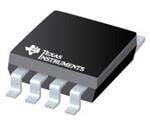
ICGOO电子元器件商城为您提供SN74LVC3G07QDCURQ1由Texas Instruments设计生产,在icgoo商城现货销售,并且可以通过原厂、代理商等渠道进行代购。 SN74LVC3G07QDCURQ1价格参考¥1.22-¥3.50。Texas InstrumentsSN74LVC3G07QDCURQ1封装/规格:逻辑 - 缓冲器,驱动器,接收器,收发器, Buffer, Non-Inverting 3 Element 1 Bit per Element Open Drain Output US8。您可以下载SN74LVC3G07QDCURQ1参考资料、Datasheet数据手册功能说明书,资料中有SN74LVC3G07QDCURQ1 详细功能的应用电路图电压和使用方法及教程。
| 参数 | 数值 |
| 产品目录 | 集成电路 (IC)半导体 |
| 描述 | IC BUFF/DVR TRPL N-INV US8缓冲器和线路驱动器 Dual 1-Of-4 FET Mltplxr/Demltplxr |
| 产品分类 | |
| 品牌 | Texas Instruments |
| 产品手册 | |
| 产品图片 |
|
| rohs | 符合RoHS无铅 / 符合限制有害物质指令(RoHS)规范要求 |
| 产品系列 | 逻辑集成电路,缓冲器和线路驱动器,Texas Instruments SN74LVC3G07QDCURQ174LVC |
| 数据手册 | |
| 产品型号 | SN74LVC3G07QDCURQ1 |
| 产品目录页面 | |
| 产品种类 | 缓冲器和线路驱动器 |
| 传播延迟时间 | 3.7 ns at 3.3 V, 2.9 ns at 5 V |
| 低电平输出电流 | 32 mA |
| 供应商器件封装 | US8 |
| 元件数 | 3 |
| 其它名称 | 296-23710-1 |
| 包装 | 剪切带 (CT) |
| 单位重量 | 9.600 mg |
| 商标 | Texas Instruments |
| 安装类型 | 表面贴装 |
| 安装风格 | SMD/SMT |
| 封装 | Reel |
| 封装/外壳 | 8-VFSOP(0.091",2.30mm 宽) |
| 封装/箱体 | VSSOP-8 |
| 工作温度 | -40°C ~ 125°C |
| 工厂包装数量 | 3000 |
| 最大工作温度 | + 125 C |
| 最小工作温度 | - 40 C |
| 极性 | Non-Inverting |
| 标准包装 | 1 |
| 每元件位数 | 1 |
| 每芯片的通道数量 | 3 |
| 电压-电源 | 1.65 V ~ 5.5 V |
| 电流-输出高,低 | -,32mA |
| 电源电压-最大 | 5.5 V |
| 电源电压-最小 | 1.65 V |
| 系列 | SN74LVC3G07-Q1 |
| 输入线路数量 | 1 |
| 输出类型 | Open Drain |
| 输出线路数量 | 1 |
| 逻辑类型 | 缓冲器/线路驱动器,非反相并带开漏极 |
| 逻辑系列 | LVC |


- 商务部:美国ITC正式对集成电路等产品启动337调查
- 曝三星4nm工艺存在良率问题 高通将骁龙8 Gen1或转产台积电
- 太阳诱电将投资9.5亿元在常州建新厂生产MLCC 预计2023年完工
- 英特尔发布欧洲新工厂建设计划 深化IDM 2.0 战略
- 台积电先进制程称霸业界 有大客户加持明年业绩稳了
- 达到5530亿美元!SIA预计今年全球半导体销售额将创下新高
- 英特尔拟将自动驾驶子公司Mobileye上市 估值或超500亿美元
- 三星加码芯片和SET,合并消费电子和移动部门,撤换高东真等 CEO
- 三星电子宣布重大人事变动 还合并消费电子和移动部门
- 海关总署:前11个月进口集成电路产品价值2.52万亿元 增长14.8%


PDF Datasheet 数据手册内容提取
SN74LVC3G07-Q1 www.ti.com.................................................................................................................................................... SCES616B–OCTOBER2004–REVISEDAPRIL2008 TRIPLE BUFFER/DRIVER WITH OPEN-DRAIN OUTPUTS FEATURES 1 • QualifiedforAutomotiveApplications • TypicalV (OutputV Undershoot)>2Vat OHV OH • Supports5-VVCCOperation VCC=3.3V,TA=25(cid:176) C • Maxtpdof3.7nsat3.3V • IoffSupportsPartial-Power-DownMode • LowPowerConsumption,10-m AMaxI Operation CC • ±24-mAOutputDriveat3.3V • Latch-UpPerformanceExceeds100mAPer JESD78,ClassII • InputandOpen-DrainOutputAccepts • ESDProtectionExceedsJESD22 Voltagesupto5.5V • TypicalV (OutputGroundBounce)<0.8Vat – 2000-VHuman-BodyModel(A114-A) OLP V =3.3V,T =25(cid:176) C – 200-VMachineModel(A115-A) CC A – 1000-VCharged-DeviceModel(C101) DCU PACKAGE (TOPVIEW) 1A 1 8 V CC 3Y 2 7 1Y 2A 3 6 3A GND 4 5 2Y See mechanical drawing for dimensions. DESCRIPTION/ORDERING INFORMATION Thistriplebuffer/driverisdesignedfor1.65-Vto5.5-VV operation. CC The output of the SN74LVC3G07 is open drain and can be connected to other open-drain outputs to implement active-lowwired-ORoractive-highwired-ANDfunctions.Themaximumsinkcurrentis32mA. This device is fully specified for partial-power-down applications using I . The I circuitry disables the outputs, off off preventingdamagingcurrentbackflowthroughthedevicewhenitispowereddown. ORDERINGINFORMATION(1) T PACKAGE(2) ORDERABLEPARTNUMBER TOP-SIDEMARKING(3) A –40(cid:176) Cto125(cid:176) C VSSOP–DCU Reelof3000 SN74LVC3G07QDCURQ1 C07_ (1) Forthemostcurrentpackageandorderinginformation,seethePackageOptionAddendumattheendofthisdocument,orseetheTI websiteatwww.ti.com. (2) Packagedrawings,thermaldata,andsymbolizationareavailableatwww.ti.com/packaging. (3) DCU:Theactualtop-sidemarkinghasoneadditionalcharacterthatdesignatesthewaferfab/assemblysite. FUNCTIONTABLE (EACHBUFFER/DRIVER) INPUT OUTPUT A Y H H L L 1 Pleasebeawarethatanimportantnoticeconcerningavailability,standardwarranty,anduseincriticalapplicationsof TexasInstrumentssemiconductorproductsanddisclaimerstheretoappearsattheendofthisdatasheet. PRODUCTIONDATAinformationiscurrentasofpublicationdate. Copyright©2004–2008,TexasInstrumentsIncorporated Products conform to specifications per the terms of the Texas Instruments standard warranty. Production processing does not necessarilyincludetestingofallparameters.
SN74LVC3G07-Q1 SCES616B–OCTOBER2004–REVISEDAPRIL2008.................................................................................................................................................... www.ti.com LOGICDIAGRAM(POSITIVELOGIC) 1 7 1A 1Y 3 5 2A 2Y 6 2 3A 3Y Absolute Maximum Ratings(1) overoperatingfree-airtemperaturerange(unlessotherwisenoted) MIN MAX UNIT V Supplyvoltagerange –0.5 6.5 V CC V Inputvoltagerange –0.5 6.5 V I V Voltagerangeappliedtoanyoutputinthehigh-impedanceorpower-offstate(2) –0.5 6.5 V O V Voltagerangeappliedtoanyoutputinthehighorlowstate(2)(3) –0.5 6.5 V O I Inputclampcurrent V <0 –50 mA IK I I Outputclampcurrent V <0 –50 mA OK O I Continuousoutputcurrent ±50 mA O ContinuouscurrentthroughV orGND ±100 mA CC q Packagethermalimpedance(4) 227 (cid:176) C/W JA T Storagetemperaturerange –65 150 (cid:176) C stg (1) Stressesbeyondthoselistedunder"absolutemaximumratings"maycausepermanentdamagetothedevice.Thesearestressratings only,andfunctionaloperationofthedeviceattheseoranyotherconditionsbeyondthoseindicatedunder"recommendedoperating conditions"isnotimplied.Exposuretoabsolute-maximum-ratedconditionsforextendedperiodsmayaffectdevicereliability. (2) Theinputandoutputnegative-voltageratingsmaybeexceedediftheinputandoutputcurrentratingsareobserved. (3) ThevalueofV isprovidedintherecommendedoperatingconditionstable. CC (4) ThepackagethermalimpedanceiscalculatedinaccordancewithJESD51-7. 2 SubmitDocumentationFeedback Copyright©2004–2008,TexasInstrumentsIncorporated ProductFolderLink(s):SN74LVC3G07-Q1
SN74LVC3G07-Q1 www.ti.com.................................................................................................................................................... SCES616B–OCTOBER2004–REVISEDAPRIL2008 Recommended Operating Conditions(1) MIN MAX UNIT Operating 1.65 5.5 V Supplyvoltage V CC Dataretentiononly 1.5 V =1.65Vto1.95V 0.65· V CC CC V =2.3Vto2.7V 1.7 CC V High-levelinputvoltage V IH V =3Vto3.6V 2 CC V =4.5Vto5.5V 0.7· V CC CC V =1.65Vto1.95V 0.35· V CC CC V =2.3Vto2.7V 0.7 CC V Low-levelinputvoltage V IL V =3Vto3.6V 0.8 CC V =4.5Vto5.5V 0.3· V CC CC V Inputvoltage 0 5.5 V I V Outputvoltage 0 5.5 V O V =1.65V 4 CC V =2.3V 8 CC I Low-leveloutputcurrent 16 mA OL V =3V CC 24 V =4.5V 32 CC V =1.8V±0.15V,2.5V±0.2V 20 CC Δt/Δv Inputtransitionriseorfallrate V =3.3V±0.3V 10 ns/V CC V =5V±0.5V 5 CC T Operatingfree-airtemperature –40 125 (cid:176) C A (1) AllunusedinputsofthedevicemustbeheldatV orGNDtoensureproperdeviceoperation.RefertotheTIapplicationreport, CC ImplicationsofSloworFloatingCMOSInputs,literaturenumberSCBA004. Electrical Characteristics overrecommendedoperatingfree-airtemperaturerange(unlessotherwisenoted) PARAMETER TESTCONDITIONS V MIN TYP(1) MAX UNIT CC I =100m A 1.65Vto5.5V 0.1 OL I =4mA 1.65V 0.45 OL I =8mA 2.3V 0.3 OL I =16mA 3V 0.4 OL V V OL T =–40(cid:176) Cto85(cid:176) C 0.55 A I =24mA 3V OL T =125(cid:176) C 0.6 A T =–40(cid:176) Cto85(cid:176) C 0.55 A I =32mA 4.5V OL T =125(cid:176) C 0.65 A I Ainputs V =5.5VorGND 0to5.5V ±5 m A I I I V orV =5.5V 0 ±10 m A off I O I V =5.5VorGND, I =0 1.65Vto5.5V 10 m A CC I O ΔI OneinputatV –0.6V, OtherinputsatV orGND 3Vto5.5V 500 m A CC CC CC C V =V orGND 3.3V 3.5 pF i I CC (1) AlltypicalvaluesareatV =3.3V,T =25(cid:176) C. CC A Copyright©2004–2008,TexasInstrumentsIncorporated SubmitDocumentationFeedback 3 ProductFolderLink(s):SN74LVC3G07-Q1
SN74LVC3G07-Q1 SCES616B–OCTOBER2004–REVISEDAPRIL2008.................................................................................................................................................... www.ti.com Switching Characteristics overrecommendedoperatingfree-airtemperaturerange(unlessotherwisenoted)(seeFigure1) V =1.8V V =2.5V V =3.3V V =5V CC CC CC CC PARAMETER FROM TO ±0.15V ±0.2V ±0.3V ±0.5V UNIT (INPUT) (OUTPUT) MIN MAX MIN MAX MIN MAX MIN MAX t A Y 1.5 7.8 1 4.3 1.1 3.7 1 2.9 ns pd Operating Characteristics T =25(cid:176) C A V =1.8V V =2.5V V =3.3V V =5V CC CC CC CC PARAMETER TESTCONDITIONS UNIT TYP TYP TYP TYP C Powerdissipationcapacitance f=10MHz 3 3 4 5 pF pd 4 SubmitDocumentationFeedback Copyright©2004–2008,TexasInstrumentsIncorporated ProductFolderLink(s):SN74LVC3G07-Q1
SN74LVC3G07-Q1 www.ti.com.................................................................................................................................................... SCES616B–OCTOBER2004–REVISEDAPRIL2008 PARAMETER MEASUREMENT INFORMATION (OPEN DRAIN) VLOAD From Output RL S1 Open TEST S1 Under Test GND tPZL (see Notes E and F) VLOAD CL (see Note A) RL tPLZ (see Notes E and G) VLOAD tPHZ/tPZH VLOAD LOAD CIRCUIT INPUT VCC VI tr/tf VM VLOAD CL RL VD 1.8 V ± 0.15 V VCC ≤ 2 ns VCC/2 2 × VCC 30 pF 1 kW 0.15 V 2.5 V ± 0.2 V VCC ≤ 2 ns VCC/2 2 × VCC 30 pF 500 W 0.15 V 3.3 V ± 0.3 V 3 V ≤ 2.5 ns 1.5 V 6 V 50 pF 500 W 0.3 V 5 V ± 0.5 V VCC ≤ 2.5 ns VCC/2 2 × VCC 50 pF 500 W 0.3 V VI Timing Input VM 0 V tw tsu th VI Input VM VM Data Input VM VM VI 0 V 0 V VOLTAGE WAVEFORMS VOLTAGE WAVEFORMS PULSE DURATION SETUP AND HOLD TIMES VI Output VI Input VM VM Control VM VM 0 V 0 V tPLH tPHL Output tPZL tPLZ VOH Waveform 1 VLOAD/2 Output VM VM VOL (Ss1e ea tN VoLteO ABD) VM VOL + VD VOL tPHL tPLH tPZH tPHZ Output Output VM VM VOH WS1a vaet fVoLrOmA D2 VM VLOAD/2 - VD VLOAD/2 VOL (see Note B) ≈0 V VOLTAGE WAVEFORMS VOLTAGE WAVEFORMS PROPAGATION DELAY TIMES ENABLE AND DISABLE TIMES INVERTING AND NONINVERTING OUTPUTS LOW- AND HIGH-LEVEL ENABLING NOTES: A. CL includes probe and jig capacitance. B. Waveform 1 is for an output with internal conditions such that the output is low, except when disabled by the output control. Waveform2 is for an output with internal conditions such that the output is high, except when disabled by the output control. C. All input pulses are supplied by generators having the following characteristics: PRR ≤ 10 MHz, ZO = 50 W . D. The outputs are measured one at a time, with one transition per measurement. E. Since this device has open-drain outputs, tPLZ and tPZL are the same as tpd. F. tPZL is measured at VM. G. tPLZ is measured at VOL + VD . H. All parameters and waveforms are not applicable to all devices. Figure1.LoadCircuitandVoltageWaveforms Copyright©2004–2008,TexasInstrumentsIncorporated SubmitDocumentationFeedback 5 ProductFolderLink(s):SN74LVC3G07-Q1
PACKAGE OPTION ADDENDUM www.ti.com 6-Feb-2020 PACKAGING INFORMATION Orderable Device Status Package Type Package Pins Package Eco Plan Lead/Ball Finish MSL Peak Temp Op Temp (°C) Device Marking Samples (1) Drawing Qty (2) (6) (3) (4/5) CLVC3G07QDCURG4Q1 ACTIVE VSSOP DCU 8 3000 Green (RoHS NIPDAU Level-1-260C-UNLIM -40 to 125 C07R & no Sb/Br) SN74LVC3G07QDCURQ1 ACTIVE VSSOP DCU 8 3000 Green (RoHS NIPDAU Level-1-260C-UNLIM -40 to 125 C07R & no Sb/Br) (1) The marketing status values are defined as follows: ACTIVE: Product device recommended for new designs. LIFEBUY: TI has announced that the device will be discontinued, and a lifetime-buy period is in effect. NRND: Not recommended for new designs. Device is in production to support existing customers, but TI does not recommend using this part in a new design. PREVIEW: Device has been announced but is not in production. Samples may or may not be available. OBSOLETE: TI has discontinued the production of the device. (2) RoHS: TI defines "RoHS" to mean semiconductor products that are compliant with the current EU RoHS requirements for all 10 RoHS substances, including the requirement that RoHS substance do not exceed 0.1% by weight in homogeneous materials. Where designed to be soldered at high temperatures, "RoHS" products are suitable for use in specified lead-free processes. TI may reference these types of products as "Pb-Free". RoHS Exempt: TI defines "RoHS Exempt" to mean products that contain lead but are compliant with EU RoHS pursuant to a specific EU RoHS exemption. Green: TI defines "Green" to mean the content of Chlorine (Cl) and Bromine (Br) based flame retardants meet JS709B low halogen requirements of <=1000ppm threshold. Antimony trioxide based flame retardants must also meet the <=1000ppm threshold requirement. (3) MSL, Peak Temp. - The Moisture Sensitivity Level rating according to the JEDEC industry standard classifications, and peak solder temperature. (4) There may be additional marking, which relates to the logo, the lot trace code information, or the environmental category on the device. (5) Multiple Device Markings will be inside parentheses. Only one Device Marking contained in parentheses and separated by a "~" will appear on a device. If a line is indented then it is a continuation of the previous line and the two combined represent the entire Device Marking for that device. (6) Lead/Ball Finish - Orderable Devices may have multiple material finish options. Finish options are separated by a vertical ruled line. Lead/Ball Finish values may wrap to two lines if the finish value exceeds the maximum column width. Important Information and Disclaimer:The information provided on this page represents TI's knowledge and belief as of the date that it is provided. TI bases its knowledge and belief on information provided by third parties, and makes no representation or warranty as to the accuracy of such information. Efforts are underway to better integrate information from third parties. TI has taken and continues to take reasonable steps to provide representative and accurate information but may not have conducted destructive testing or chemical analysis on incoming materials and chemicals. TI and TI suppliers consider certain information to be proprietary, and thus CAS numbers and other limited information may not be available for release. In no event shall TI's liability arising out of such information exceed the total purchase price of the TI part(s) at issue in this document sold by TI to Customer on an annual basis. Addendum-Page 1
PACKAGE OPTION ADDENDUM www.ti.com 6-Feb-2020 OTHER QUALIFIED VERSIONS OF SN74LVC3G07-Q1 : •Catalog: SN74LVC3G07 •Enhanced Product: SN74LVC3G07-EP NOTE: Qualified Version Definitions: •Catalog - TI's standard catalog product •Enhanced Product - Supports Defense, Aerospace and Medical Applications Addendum-Page 2
PACKAGE MATERIALS INFORMATION www.ti.com 3-Aug-2017 TAPE AND REEL INFORMATION *Alldimensionsarenominal Device Package Package Pins SPQ Reel Reel A0 B0 K0 P1 W Pin1 Type Drawing Diameter Width (mm) (mm) (mm) (mm) (mm) Quadrant (mm) W1(mm) SN74LVC3G07QDCURQ1 VSSOP DCU 8 3000 180.0 8.4 2.25 3.35 1.05 4.0 8.0 Q3 PackMaterials-Page1
PACKAGE MATERIALS INFORMATION www.ti.com 3-Aug-2017 *Alldimensionsarenominal Device PackageType PackageDrawing Pins SPQ Length(mm) Width(mm) Height(mm) SN74LVC3G07QDCURQ1 VSSOP DCU 8 3000 202.0 201.0 28.0 PackMaterials-Page2
None
None
IMPORTANTNOTICEANDDISCLAIMER TI PROVIDES TECHNICAL AND RELIABILITY DATA (INCLUDING DATASHEETS), DESIGN RESOURCES (INCLUDING REFERENCE DESIGNS), APPLICATION OR OTHER DESIGN ADVICE, WEB TOOLS, SAFETY INFORMATION, AND OTHER RESOURCES “AS IS” AND WITH ALL FAULTS, AND DISCLAIMS ALL WARRANTIES, EXPRESS AND IMPLIED, INCLUDING WITHOUT LIMITATION ANY IMPLIED WARRANTIES OF MERCHANTABILITY, FITNESS FOR A PARTICULAR PURPOSE OR NON-INFRINGEMENT OF THIRD PARTY INTELLECTUAL PROPERTY RIGHTS. These resources are intended for skilled developers designing with TI products. You are solely responsible for (1) selecting the appropriate TI products for your application, (2) designing, validating and testing your application, and (3) ensuring your application meets applicable standards, and any other safety, security, or other requirements. These resources are subject to change without notice. TI grants you permission to use these resources only for development of an application that uses the TI products described in the resource. Other reproduction and display of these resources is prohibited. No license is granted to any other TI intellectual property right or to any third party intellectual property right. TI disclaims responsibility for, and you will fully indemnify TI and its representatives against, any claims, damages, costs, losses, and liabilities arising out of your use of these resources. TI’s products are provided subject to TI’s Terms of Sale (www.ti.com/legal/termsofsale.html) or other applicable terms available either on ti.com or provided in conjunction with such TI products. TI’s provision of these resources does not expand or otherwise alter TI’s applicable warranties or warranty disclaimers for TI products. Mailing Address: Texas Instruments, Post Office Box 655303, Dallas, Texas 75265 Copyright © 2020, Texas Instruments Incorporated