ICGOO在线商城 > 集成电路(IC) > 逻辑 - 缓冲器,驱动器,接收器,收发器 > SN74LVC1G125DRLR
 Datasheet下载
- 型号: SN74LVC1G125DRLR
- 制造商: Texas Instruments
- 库位|库存: xxxx|xxxx
- 要求:
| 数量阶梯 | 香港交货 | 国内含税 |
| +xxxx | $xxxx | ¥xxxx |
查看当月历史价格
查看今年历史价格
SN74LVC1G125DRLR产品简介:
ICGOO电子元器件商城为您提供SN74LVC1G125DRLR由Texas Instruments设计生产,在icgoo商城现货销售,并且可以通过原厂、代理商等渠道进行代购。 SN74LVC1G125DRLR价格参考。Texas InstrumentsSN74LVC1G125DRLR封装/规格:逻辑 - 缓冲器,驱动器,接收器,收发器, Buffer, Non-Inverting 1 Element 1 Bit per Element 3-State Output SOT-5。您可以下载SN74LVC1G125DRLR参考资料、Datasheet数据手册功能说明书,资料中有SN74LVC1G125DRLR 详细功能的应用电路图电压和使用方法及教程。
| 参数 | 数值 |
| 产品目录 | 集成电路 (IC)半导体 |
| 描述 | IC BUS BUFF TRI-ST N-INV SOT5缓冲器和线路驱动器 Single Bus Buffer Gate |
| 产品分类 | |
| 品牌 | Texas Instruments |
| 产品手册 | http://www.ti.com/lit/gpn/sn74lvc1g125 |
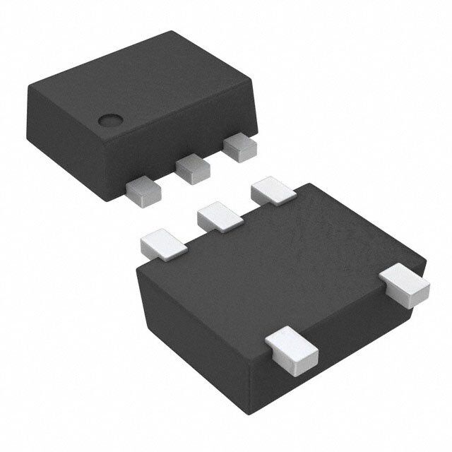
| 产品图片 |
|
| rohs | 符合RoHS无铅 / 符合限制有害物质指令(RoHS)规范要求 |
| 产品系列 | 逻辑集成电路,缓冲器和线路驱动器,Texas Instruments SN74LVC1G125DRLR74LVC |
| 数据手册 | |
| 产品型号 | SN74LVC1G125DRLR |
| 产品目录页面 | |
| 产品种类 | 缓冲器和线路驱动器 |
| 传播延迟时间 | 4.5 ns at 3.3 V, 4 ns at 5 V |
| 低电平输出电流 | 32 mA |
| 供应商器件封装 | SOT-5 |
| 元件数 | 1 |
| 其它名称 | 296-18012-1 |
| 包装 | 剪切带 (CT) |
| 单位重量 | 2.800 mg |
| 商标 | Texas Instruments |
| 安装类型 | 表面贴装 |
| 安装风格 | SMD/SMT |
| 封装 | Reel |
| 封装/外壳 | SOT-553 |
| 封装/箱体 | SOT-553-5 |
| 工作温度 | -40°C ~ 125°C |
| 工厂包装数量 | 4000 |
| 最大工作温度 | + 85 C |
| 最小工作温度 | - 40 C |
| 极性 | Non-Inverting |
| 标准包装 | 1 |
| 每元件位数 | 1 |
| 每芯片的通道数量 | 1 |
| 电压-电源 | 1.65 V ~ 5.5 V |
| 电流-输出高,低 | 32mA,32mA |
| 电源电压-最大 | 5.5 V |
| 电源电压-最小 | 1.65 V |
| 系列 | SN74LVC1G125 |
| 输入线路数量 | 1 |
| 输出类型 | 3-State |
| 输出线路数量 | 1 |
| 逻辑类型 | 缓冲器/线路驱动器,非反相 |
| 逻辑系列 | LVC |
| 高电平输出电流 | - 32 mA |


- 商务部:美国ITC正式对集成电路等产品启动337调查
- 曝三星4nm工艺存在良率问题 高通将骁龙8 Gen1或转产台积电
- 太阳诱电将投资9.5亿元在常州建新厂生产MLCC 预计2023年完工
- 英特尔发布欧洲新工厂建设计划 深化IDM 2.0 战略
- 台积电先进制程称霸业界 有大客户加持明年业绩稳了
- 达到5530亿美元!SIA预计今年全球半导体销售额将创下新高
- 英特尔拟将自动驾驶子公司Mobileye上市 估值或超500亿美元
- 三星加码芯片和SET,合并消费电子和移动部门,撤换高东真等 CEO
- 三星电子宣布重大人事变动 还合并消费电子和移动部门
- 海关总署:前11个月进口集成电路产品价值2.52万亿元 增长14.8%


PDF Datasheet 数据手册内容提取
Product Sample & Technical Tools & Support & Folder Buy Documents Software Community SN74LVC1G125 SCES223T–APRIL1999–REVISEDOCTOBER2014 SN74LVC1G125 Single Bus Buffer Gate With 3-State Output 1 Features 3 Description • AvailableintheUltraSmall0.64-mm2 This bus buffer gate is designed for 1.65-V to 5.5-V 1 V operation. Package(DPW)With0.5-mmPitch CC • Supports5-VV Operation The SN74LVC1G125 device is a single line driver CC with a 3-state output. The output is disabled when the • InputsAcceptVoltagesto5.5V output-enable(OE)inputishigh. • ProvidesDownTranslationtoV CC The CMOS device has high output drive while • Maxt of3.7nsat3.3V pd maintaining low static power dissipation over a broad • LowPowerConsumption,10-μAMaxICC VCCoperatingrange. • ±24-mAOutputDriveat3.3V The SN74LVC1G125 device is available in a variety • IoffSupportsLiveInsertion,Partial-Power-Down of packages including the ultra-small DPW package Mode,andBack-DriveProtection withabodysizeof0.8mm ×0.8mm. • Latch-UpPerformanceExceeds100mA PerJESD78,ClassII DeviceInformation(1) • ESDProtectionExceedsJESD22 DEVICENAME PACKAGE BODYSIZE(NOM) SOT-23(5) 2.90mm×1.60mm – 2000-VHuman-BodyModel(A114-A) SC70(5) 2.00mm×1.25mm – 200-VMachineModel(A115-A) SN74LVC1G125 SON(6) 1.45mm×1.00mm – 1000-VCharged-DeviceModel(C101) DSBGA(5) 1.40mm×0.90mm 2 Applications X2SON(4) 0.80mm×0.80mm (1) For all available packages, see the orderable addendum at • CableModemTerminationSystem theendofthedatasheet. • High-SpeedDataAcquisitionandGeneration • Military:RadarandSonar • MotorControl:High-Voltage • PowerLineCommunicationModem • SSD:InternalorExternal • VideoBroadcastingandInfrastructure: ScalablePlatform • VideoBroadcasting:IP-BasedMulti-Format Transcoder • VideoCommunicationsSystem 4 Simplified Schematic 1 An IMPORTANT NOTICE at the end of this data sheet addresses availability, warranty, changes, use in safety-critical applications, intellectualpropertymattersandotherimportantdisclaimers.PRODUCTIONDATA.
SN74LVC1G125 SCES223T–APRIL1999–REVISEDOCTOBER2014 www.ti.com Table of Contents 1 Features.................................................................. 1 9 DetailedDescription............................................ 10 2 Applications........................................................... 1 9.1 Overview.................................................................10 3 Description............................................................. 1 9.2 FunctionalBlockDiagram.......................................10 4 SimplifiedSchematic............................................. 1 9.3 FeatureDescription.................................................10 9.4 DeviceFunctionalModes........................................10 5 RevisionHistory..................................................... 2 10 ApplicationandImplementation........................ 11 6 PinConfigurationandFunctions......................... 3 10.1 ApplicationInformation..........................................11 7 Specifications......................................................... 4 10.2 TypicalApplication ...............................................11 7.1 AbsoluteMaximumRatings .....................................4 11 PowerSupplyRecommendations..................... 12 7.2 HandlingRatings.......................................................4 12 Layout................................................................... 12 7.3 RecommendedOperatingConditions......................5 7.4 ThermalInformation..................................................5 12.1 LayoutGuidelines.................................................12 7.5 ElectricalCharacteristics...........................................6 12.2 LayoutExample....................................................12 7.6 SwitchingCharacteristics,C =15pF......................6 13 DeviceandDocumentationSupport................. 13 L 7.7 SwitchingCharacteristics,–40°Cto85°C.................6 13.1 Trademarks...........................................................13 7.8 SwitchingCharacteristics,–40°Cto125°C...............7 13.2 ElectrostaticDischargeCaution............................13 7.9 OperatingCharacteristics..........................................7 13.3 Glossary................................................................13 7.10 TypicalCharacteristics............................................7 14 Mechanical,Packaging,andOrderable Information........................................................... 13 8 ParameterMeasurementInformation..................8 5 Revision History ChangesfromRevisionS(April2014)toRevisionT Page • UpdatedDeviceInformationtable. ........................................................................................................................................ 1 • RemovedPREVIEWstatusfromDPWPinOutdrawing. ..................................................................................................... 3 ChangesfromRevisionR(April2013)toRevisionS Page • AddedApplications................................................................................................................................................................. 1 • AddedPinFunctionstable..................................................................................................................................................... 3 • UpdatedHandlingRatingstable. ........................................................................................................................................... 4 • AddedThermalInformationtable. ......................................................................................................................................... 5 • AddedTypicalCharacteristics. .............................................................................................................................................. 7 • AddedDetailedDescriptionsection..................................................................................................................................... 10 • AddedApplicationandImplementationsection. ................................................................................................................. 11 • AddedPowerSupplyRecommendationssection. .............................................................................................................. 12 • AddedLayoutsection. ......................................................................................................................................................... 12 ChangesfromRevisionQ(November2012)toRevisionR Page • AddedDeviceInformationtable............................................................................................................................................. 1 • MovedT toHandlingRatingstable..................................................................................................................................... 4 stg • Added–40°Cto125°CTemperaturerangetoElectricalCharacteristics............................................................................... 6 • AddedSwitchingCharacteristicsfor–40°Cto125°Ctemperaturerange. ............................................................................ 7 2 SubmitDocumentationFeedback Copyright©1999–2014,TexasInstrumentsIncorporated ProductFolderLinks:SN74LVC1G125
SN74LVC1G125 www.ti.com SCES223T–APRIL1999–REVISEDOCTOBER2014 6 Pin Configuration and Functions DBV PACKAGE DCK PACKAGE DRLPACKAGE DRYPACKAGE (TOPVIEW) (TOPVIEW) (TOPVIEW) (TOPVIEW) OE 1 5 V OE 1 5 VCC OE 1 5 VCC OE 1 6 VCC CC A 2 A 2 5 N.C. A 2 A 2 GND 3 4 Y GND 3 4 Y GND 3 4 Y GND 3 4 Y DPW PACKAGE DSF PACKAGE YZPPACKAGE (TOPVIEW) (TOPVIEW) (BOTTOM VIEW) GND OE 1 3 5 VCC OE 1 6 VCC GND C134C2 Y A 2 4 Y A 2 5 N.C. A B12 GND 3 4 Y OE A115A2 VCC N.C.–Nointernalconnection Seemechanicaldrawingsfordimensions. PinFunctions PIN DRL,DCK, DESCRIPTION NAME DRY,DSF DPW YZP DBV OE 1 1 1 A1 Input A 2 2 2 B1 Input GND 3 3 3 C1 Ground Y 4 4 4 C2 Output VCC 5 6 5 A2 Powerpin NC – 5 – – Notconnected Copyright©1999–2014,TexasInstrumentsIncorporated SubmitDocumentationFeedback 3 ProductFolderLinks:SN74LVC1G125
SN74LVC1G125 SCES223T–APRIL1999–REVISEDOCTOBER2014 www.ti.com 7 Specifications 7.1 Absolute Maximum Ratings(1) overoperatingfree-airtemperaturerange(unlessotherwisenoted) MIN MAX UNIT V Supplyvoltagerange –0.5 6.5 V CC V Inputvoltagerange(2) –0.5 6.5 V I V Voltagerangeappliedtoanyoutputinthehigh-impedanceorpower-offstate(2) –0.5 6.5 V O V Voltagerangeappliedtoanyoutputinthehighorlowstate(2)(3) –0.5 V +0.5 V O CC I Inputclampcurrent V <0 –50 mA IK I I Outputclampcurrent V <0 –50 mA OK O I Continuousoutputcurrent ±50 mA O ContinuouscurrentthroughV orGND ±100 mA CC (1) StressesbeyondthoselistedunderAbsoluteMaximumRatingsmaycausepermanentdamagetothedevice.Thesearestressratings only,andfunctionaloperationofthedeviceattheseoranyotherconditionsbeyondthoseindicatedunderRecommendedOperatingis notimplied.Exposuretoabsolute-maximum-ratedconditionsforextendedperiodsmayaffectdevicereliability. (2) Theinputandoutputnegative-voltageratingsmaybeexceedediftheinputandoutputcurrentratingsareobserved. (3) ThevalueofV isprovidedintheRecommendedOperatingtable. CC 7.2 Handling Ratings MIN MAX UNIT T Storagetemperaturerange –65 150 °C stg Humanbodymodel(HBM),perANSI/ESDA/JEDECJS-001,all pins(1) 0 2000 V Electrostaticdischarge V (ESD) Chargeddevicemodel(CDM),perJEDECspecification JESD22-C101,allpins(2) 0 1000 (1) JEDECdocumentJEP155statesthat500-VHBMallowssafemanufacturingwithastandardESDcontrolprocess. (2) JEDECdocumentJEP157statesthat250-VCDMallowssafemanufacturingwithastandardESDcontrolprocess. 4 SubmitDocumentationFeedback Copyright©1999–2014,TexasInstrumentsIncorporated ProductFolderLinks:SN74LVC1G125
SN74LVC1G125 www.ti.com SCES223T–APRIL1999–REVISEDOCTOBER2014 7.3 Recommended Operating Conditions(1) MIN MAX UNIT Operating 1.65 5.5 V Supplyvoltage V CC Dataretentiononly 1.5 V =1.65Vto1.95V 0.65×V CC CC V =2.3Vto2.7V 1.7 CC V High-levelinputvoltage V IH V =3Vto3.6V 2 CC V =4.5Vto5.5V 0.7×V CC CC V =1.65Vto1.95V 0.35×V CC CC V =2.3Vto2.7V 0.7 CC V Low-levelinputvoltage V IL V =3Vto3.6V 0.8 CC V =4.5Vto5.5V 0.3×V CC CC V Inputvoltage 0 5.5 V I V Outputvoltage 0 V V O CC V =1.65V –4 CC V =2.3V –8 CC I High-leveloutputcurrent –16 mA OH V =3V CC –24 V =4.5V –32 CC V =1.65V 4 CC V =2.3V 8 CC I Low-leveloutputcurrent 16 mA OL V =3V CC 24 V =4.5V 32 CC V =1.8V±0.15V,2.5V±0.2V 20 CC Δt/Δv Inputtransitionriseorfallrate V =3.3V±0.3V 10 ns/V CC V =5V±0.5V 5 CC T Operatingfree-airtemperature –40 125 °C A (1) AllunusedinputsofthedevicemustbeheldatV orGNDtoensureproperdeviceoperation.RefertotheTIapplicationreport, CC ImplicationsofSloworFloatingCMOSInputs,literaturenumberSCBA004. 7.4 Thermal Information SN74LVC1G125 THERMALMETRIC(1) DBV DCK DRL DRY YZP DPW UNIT 5PINS 5PINS 5PINS 6PINS 5PINS 4PINS RθJA Junction-to-ambientthermalresistance 229 278 243 439 130 340 RθJC(top) Junction-to-case(top)thermalresistance 164 93 78 277 54 215 RθJB Junction-to-boardthermalresistance 62 65 78 271 51 294 °C/W ψJT Junction-to-topcharacterizationparameter 44 2 10 84 1 41 ψJB Junction-to-boardcharacterizationparameter 62 64 77 271 50 294 RθJC(bot) Junction-to-case(bottom)thermalresistance – – – – – 250 (1) Formoreinformationabouttraditionalandnewthermalmetrics,seetheICPackageThermalMetricsapplicationreport,SPRA953. Copyright©1999–2014,TexasInstrumentsIncorporated SubmitDocumentationFeedback 5 ProductFolderLinks:SN74LVC1G125
SN74LVC1G125 SCES223T–APRIL1999–REVISEDOCTOBER2014 www.ti.com 7.5 Electrical Characteristics overrecommendedoperatingfree-airtemperaturerange(unlessotherwisenoted) –40Cto85°C –40Cto125°C PARAMETER TESTCONDITIONS V UNIT CC MIN TYP(1) MAX MIN TYP(1) MAX I =–100μA 1.65Vto5.5V V –0.1 V –0.1 OH CC CC I =–4mA 1.65V 1.2 1.2 OH I =–8mA 2.3V 1.9 1.9 OH V V OH I =–16mA 2.4 2.4 OH 3V I =–24mA 2.3 2.3 OH I =–32mA 4.5V 3.8 3.8 OH I =100μA 1.65Vto5.5V 0.1 0.1 OL I =4mA 1.65V 0.45 0.45 OL I =8mA 2.3V 0.3 0.3 OL V V OL I =16mA 0.4 0.4 OL 3V I =24mA 0.55 0.55 OL I =32mA 4.5V 0.55 0.55 OL AorOE I V =5.5VorGND 0to5.5V ±5 ±5 μA I inputs I I V orV =5.5V 0 ±10 ±10 μA off I O I V =0to5.5V 3.6V 10 10 μA OZ O I V =5.5VorGND, I =0 1.65Vto5.5V 10 10 μA CC I O OneinputatV –0.6V, ΔI CC 3Vto5.5V 500 500 μA CC OtherinputsatV orGND CC C V =V orGND 3.3V 4 4 pF I I CC (1) AlltypicalvaluesareatV =3.3V,T =25°C. CC A 7.6 Switching Characteristics, C = 15 pF L overrecommendedoperatingfree-airtemperaturerangeof–40°Cto85°C,C =15pF(unlessotherwisenoted) L (seeFigure3) V =1.8V V =2.5V V =3.3V V =5V CC CC CC CC PARAMETER FROM TO ±0.15V ±0.2V ±0.3V ±0.5V UNIT (INPUT) (OUTPUT) MIN MAX MIN MAX MIN MAX MIN MAX t A Y 1.9 6.9 0.7 4.6 0.6 3.7 0.5 3.4 ns pd 7.7 Switching Characteristics, –40°C to 85°C overrecommendedoperatingfree-airtemperaturerange–40°Cto85°C,C =30pFor50pF(unlessotherwisenoted) L (seeFigure4) V =1.8V V =2.5V V =3.3V V =5V CC CC CC CC PARAMETER FROM TO ±0.15V ±0.2V ±0.3V ±0.5V UNIT (INPUT) (OUTPUT) MIN MAX MIN MAX MIN MAX MIN MAX t A Y 2.8 9 1.2 5.5 1 4.5 1 4 ns pd t OE Y 3.3 10.1 1.5 6.6 1 5.3 1 5 ns en t OE Y 1.3 9.2 1 5 1 5 1 4.2 ns dis 6 SubmitDocumentationFeedback Copyright©1999–2014,TexasInstrumentsIncorporated ProductFolderLinks:SN74LVC1G125
SN74LVC1G125 www.ti.com SCES223T–APRIL1999–REVISEDOCTOBER2014 7.8 Switching Characteristics, –40°C to 125°C overrecommendedoperatingfree-airtemperaturerange–40°Cto125°C,C =30pFor50pF(unlessotherwisenoted) L (seeFigure4) V =1.8V V =2.5V V =3.3V V =5V CC CC CC CC PARAMETER FROM TO ±0.15V ±0.2V ±0.3V ±0.5V UNIT (INPUT) (OUTPUT) MIN MAX MIN MAX MIN MAX MIN MAX t A Y 2.8 9.3 1.2 5.8 1 4.7 1 4.2 ns pd t OE Y 3.3 10.4 1.5 6.9 1 5.6 1 5.2 ns en t OE Y 1.3 9.3 1 5.2 1 5.2 1 4.4 ns dis 7.9 Operating Characteristics T =25°C A TEST VCC=1.8V VCC=2.5V VCC=3.3V VCC=5V PARAMETER UNIT CONDITIONS TYP TYP TYP TYP Powerdissipation Outputsenabled 18 18 19 21 C f=10MHz pF pd capacitance Outputsdisabled 2 2 2 4 7.10 Typical Characteristics 2.5 5 TPD TPD 2 4 s 1.5 s 3 n n D - D - P P T 1 T 2 0.5 1 0 0 -100 -50 0 50 100 150 0 1 2 3 4 5 6 Temperature - °C Vcc - V D001 D002 Figure1.TPDAcrossTemperatureat3.3VV Figure2.TPDAcrossV at25°C CC CC Copyright©1999–2014,TexasInstrumentsIncorporated SubmitDocumentationFeedback 7 ProductFolderLinks:SN74LVC1G125
SN74LVC1G125 SCES223T–APRIL1999–REVISEDOCTOBER2014 www.ti.com 8 Parameter Measurement Information V LOAD R S1 Open From Output L TEST S1 Under Test GND t /t Open C PLH PHL (see NoteA)L RL tPLZ/tPZL VLOAD t /t GND PHZ PZH LOAD CIRCUIT INPUTS V V V C R V CC V t/t M LOAD L L D I r f 1.8 V±0.15 V V £2 ns V /2 2 ×V 15 pF 1 MW 0.15 V CC CC CC 2.5 V±0.2 V V £2 ns V /2 2 ×V 15 pF 1 MW 0.15 V CC CC CC 3.3 V±0.3 V 3 V £2.5 ns 1.5 V 6 V 15 pF 1 MW 0.3 V 5 V±0.5 V V £2.5 ns V /2 2 ×V 15 pF 1 MW 0.3 V CC CC CC V I Timing Input V M 0 V t W VI tsu th V Input V V I M M Data Input V V M M 0 V 0 V VOLTAGE WAVEFORMS VOLTAGE WAVEFORMS PULSE DURATION SETUPAND HOLD TIMES Input VM VM VI COounttpruotl VM VM VI 0 V 0 V t t t t PLH PHL PZL PLZ V Output V /2 Output VM VM OH WSav1e afot rVm 1 VM V + V LOAD VOL (see NoteL OBAD) OL D VOL t t PHL PLH t t PZH PHZ Output VM VM VOH WSa1v eaOfto uGrtmpNu D2t VM VOH–VD VOH VOL (see Note B) »0 V VOLTAGE WAVEFORMS VOLTAGE WAVEFORMS PROPAGATION DELAYTIMES ENABLEAND DISABLE TIMES INVERTINGAND NONINVERTING OUTPUTS LOW-AND HIGH-LEVELENABLING NOTES: A. C includes probe and jig capacitance. L B. Waveform 1 is for an output with internal conditions such that the output is low, except when disabled by the output control. Waveform 2 is for an output with internal conditions such that the output is high, except when disabled by the output control. C. All input pulses are supplied by generators having the following characteristics: PRR£10 MHz, Z = 50W. O D. The outputs are measured one at a time, with one transition per measurement. E. t and t are the same as t . PLZ PHZ dis F. t and t are the same as t . PZL PZH en G.t and t are the same as t . PLH PHL pd H. All parameters and waveforms are not applicable to all devices. Figure3. LoadCircuitandVoltageWaveforms 8 SubmitDocumentationFeedback Copyright©1999–2014,TexasInstrumentsIncorporated ProductFolderLinks:SN74LVC1G125
SN74LVC1G125 www.ti.com SCES223T–APRIL1999–REVISEDOCTOBER2014 Parameter Measurement Information (continued) V LOAD R S1 Open From Output L TEST S1 Under Test GND t /t Open C PLH PHL (see NoteA)L RL tPLZ/tPZL VLOAD t /t GND PHZ PZH LOAD CIRCUIT INPUTS V V V C R V CC V t/t M LOAD L L D I r f 1.8 V±0.15 V V £2 ns V /2 2 ×V 30 pF 1 kW 0.15 V CC CC CC 2.5 V±0.2 V V £2 ns V /2 2 ×V 30 pF 500W 0.15 V CC CC CC 3.3 V±0.3 V 3 V £2.5 ns 1.5 V 6 V 50 pF 500W 0.3 V 5 V±0.5 V V £2.5 ns V /2 2 ×V 50 pF 500W 0.3 V CC CC CC V I Timing Input V M 0 V t W VI tsu th V Input V V I M M Data Input V V M M 0 V 0 V VOLTAGE WAVEFORMS VOLTAGE WAVEFORMS PULSE DURATION SETUPAND HOLD TIMES Input VM VM VI COounttpruotl VM VM VI 0 V 0 V t t t t PLH PHL PZL PLZ V Output V /2 Output VM VM OH WSav1e afot rVm 1 VM V + V LOAD VOL (see NoteL OBAD) OL D VOL t t PHL PLH t t PZH PHZ Output VM VM VOH WSa1v eaOfto uGrtmpNu D2t VM VOH–VD VOH VOL (see Note B) »0 V VOLTAGE WAVEFORMS VOLTAGE WAVEFORMS PROPAGATION DELAYTIMES ENABLEAND DISABLE TIMES INVERTINGAND NONINVERTING OUTPUTS LOW-AND HIGH-LEVELENABLING NOTES: A. C includes probe and jig capacitance. L B. Waveform 1 is for an output with internal conditions such that the output is low, except when disabled by the output control. Waveform 2 is for an output with internal conditions such that the output is high, except when disabled by the output control. C. All input pulses are supplied by generators having the following characteristics: PRR£10 MHz, Z = 50W. O D. The outputs are measured one at a time, with one transition per measurement. E. t and t are the same as t . PLZ PHZ dis F. t and t are the same as t . PZL PZH en G.t and t are the same as t . PLH PHL pd H. All parameters and waveforms are not applicable to all devices. Figure4. LoadCircuitandVoltageWaveforms Copyright©1999–2014,TexasInstrumentsIncorporated SubmitDocumentationFeedback 9 ProductFolderLinks:SN74LVC1G125
SN74LVC1G125 SCES223T–APRIL1999–REVISEDOCTOBER2014 www.ti.com 9 Detailed Description 9.1 Overview The SN74LVC1G125 device contains one buffer gate device with output enable control and performs the Boolean function Y = A. This device is fully specified for partial-power-down applications using I . The I off off circuitry disables the outputs, preventing damaging current backflow through the device when it is powered down. To ensure the high-impedance state during power up or power down, OE should be tied to V through a pullup CC resistor;theminimumvalueoftheresistorisdeterminedbythecurrent-sinkingcapabilityofthedriver. The DPW package technology is a major breakthrough in IC packaging. Its tiny 0.64 mm square footprint saves significant board space over other package options while still retaining the traditional manufacturing friendly lead pitchof0.5mm. 9.2 Functional Block Diagram 9.3 Feature Description • Wideoperatingvoltagerange – Operatesfrom1.65Vto5.5V • Allowsdownvoltagetranslation • Inputsacceptvoltagesto5.5V • I featureallowsvoltagesontheinputsandoutputs,whenV is0V off CC 9.4 Device Functional Modes Table1.FunctionTable INPUTS OUTPUT OE A Y L H H L L L H X Z 10 SubmitDocumentationFeedback Copyright©1999–2014,TexasInstrumentsIncorporated ProductFolderLinks:SN74LVC1G125
SN74LVC1G125 www.ti.com SCES223T–APRIL1999–REVISEDOCTOBER2014 10 Application and Implementation 10.1 Application Information The SN74LVC1G125 device is a high drive CMOS device that can be used as a output enabled buffer with a high output drive, such as an LED application. It can produce 24 mA of drive current at 3.3 V making it Ideal for driving multiple outputs and good for high speed applications up to 100 MHz. The inputs are 5.5 V tolerant allowingittotranslatedowntoV . CC 10.2 Typical Application Buffer Function Basic LED Driver VCC VCC uC or Logic uC or Logic Wired OR uC or Logic uC or Logic uC or Logic LVC1G125 LVC1G125 Figure5. ApplicationSchematic 10.2.1 DesignRequirements This device uses CMOS technology and has balanced output drive. Care should be taken to avoid bus contention because it can drive currents that would exceed maximum limits. The high drive will also create fast edgesintolightloadssoroutingandloadconditionsshouldbeconsideredtopreventringing. 10.2.2 DetailedDesignProcedure 1. RecommendedInputConditions – Risetimeandfalltimespecs.See(Δt/ΔV)intheRecommendedOperatingConditionstable. – Specifiedhighandlowlevels.See(V andV )intheRecommendedOperatingConditions table. IH IL – Inputs are overvoltage tolerant allowing them to go as high as (V max) in the Recommended Operating I ConditionstableatanyvalidV . CC 2. RecommendOutputConditions – Load currents should not exceed (I max) per output and should not exceed (Continuous current through O V orGND)totalcurrentforthepart.TheselimitsarelocatedintheAbsoluteMaximumRatings table. CC – OutputsshouldnotbepulledaboveV . CC Copyright©1999–2014,TexasInstrumentsIncorporated SubmitDocumentationFeedback 11 ProductFolderLinks:SN74LVC1G125
SN74LVC1G125 SCES223T–APRIL1999–REVISEDOCTOBER2014 www.ti.com Typical Application (continued) 10.2.3 ApplicationCurves 10 Icc 1.8V 9 Icc 2.5V 8 Icc 3.3V Icc 5V 7 6 A m c - 5 Ic 4 3 2 1 0 0 20 40 60 80 Frequency - MHz D003 Figure6.I vsFrequency CC 11 Power Supply Recommendations The power supply can be any voltage between the min and max supply voltage rating located in the RecommendedOperatingConditionstable. Each VCC pin should have a good bypass capacitor to prevent power disturbance. For devices with a single supply a 0.1-μF capacitor is recommended and if there are multiple VCC pins then a 0.01-μF or 0.022-μF capacitor is recommended for each power pin. It is ok to parallel multiple bypass caps to reject different frequencies of noise. 0.1-μF and 1-μF capacitors are commonly used in parallel. The bypass capacitor should be installedasclosetothepowerpinaspossibleforbestresults. 12 Layout 12.1 Layout Guidelines When using multiple bit logic devices inputs should not ever float. In many cases, functions or parts of functions of digital logic devices are unused; for example, when only two inputs of a triple-input AND gate are used or only 3 of the 4 buffer gates are used. Such input pins should not be left unconnected because the undefined voltages attheoutsideconnectionsresultinundefinedoperationalstates.Figure7 showstherulesthatmustbeobserved under all circumstances. All unused inputs of digital logic devices must be connected to a high or low bias to prevent them from floating. The logic level that should be applied to any particular unused input depends on the function of the device. Generally they will be tied to GND or VCC, whichever makes more sense or is more convenient. 12.2 Layout Example VCC Input Unused Input Output Unused Input Output Input Figure7. PackageLayout 12 SubmitDocumentationFeedback Copyright©1999–2014,TexasInstrumentsIncorporated ProductFolderLinks:SN74LVC1G125
SN74LVC1G125 www.ti.com SCES223T–APRIL1999–REVISEDOCTOBER2014 13 Device and Documentation Support 13.1 Trademarks Alltrademarksarethepropertyoftheirrespectiveowners. 13.2 Electrostatic Discharge Caution Thesedeviceshavelimitedbuilt-inESDprotection.Theleadsshouldbeshortedtogetherorthedeviceplacedinconductivefoam duringstorageorhandlingtopreventelectrostaticdamagetotheMOSgates. 13.3 Glossary SLYZ022—TIGlossary. Thisglossarylistsandexplainsterms,acronyms,anddefinitions. 14 Mechanical, Packaging, and Orderable Information The following pages include mechanical packaging and orderable information. This information is the most current data available for the designated devices. This data is subject to change without notice and revision of thisdocument.Forbrowser-basedversionsofthisdatasheet,refertotheleft-handnavigation. Copyright©1999–2014,TexasInstrumentsIncorporated SubmitDocumentationFeedback 13 ProductFolderLinks:SN74LVC1G125
PACKAGE OPTION ADDENDUM www.ti.com 4-Apr-2019 PACKAGING INFORMATION Orderable Device Status Package Type Package Pins Package Eco Plan Lead/Ball Finish MSL Peak Temp Op Temp (°C) Device Marking Samples (1) Drawing Qty (2) (6) (3) (4/5) 74LVC1G125DBVRE4 ACTIVE SOT-23 DBV 5 3000 Green (RoHS CU NIPDAU Level-1-260C-UNLIM -40 to 125 (C255, C25F, C25J, & no Sb/Br) C25K, C25R, C 25T) 74LVC1G125DBVRG4 ACTIVE SOT-23 DBV 5 3000 Green (RoHS CU NIPDAU Level-1-260C-UNLIM -40 to 125 (C255, C25F, C25J, & no Sb/Br) C25K, C25R, C 25T) 74LVC1G125DBVTG4 ACTIVE SOT-23 DBV 5 250 Green (RoHS CU NIPDAU Level-1-260C-UNLIM -40 to 125 (C255, C25F, C25K, & no Sb/Br) C25R) 74LVC1G125DCKRE4 ACTIVE SC70 DCK 5 3000 Green (RoHS CU NIPDAU Level-1-260C-UNLIM -40 to 125 CM5 & no Sb/Br) 74LVC1G125DCKRG4 ACTIVE SC70 DCK 5 3000 Green (RoHS CU NIPDAU Level-1-260C-UNLIM -40 to 125 CM5 & no Sb/Br) 74LVC1G125DCKTE4 ACTIVE SC70 DCK 5 250 Green (RoHS CU NIPDAU Level-1-260C-UNLIM -40 to 125 CM5 & no Sb/Br) 74LVC1G125DCKTG4 ACTIVE SC70 DCK 5 250 Green (RoHS CU NIPDAU Level-1-260C-UNLIM -40 to 125 CM5 & no Sb/Br) 74LVC1G125DRLRG4 ACTIVE SOT-5X3 DRL 5 4000 Green (RoHS CU NIPDAU Level-1-260C-UNLIM -40 to 125 (CM7, CMR) & no Sb/Br) SN74LVC1G125DBVR ACTIVE SOT-23 DBV 5 3000 Green (RoHS CU NIPDAU Level-1-260C-UNLIM -40 to 125 (C255, C25F, C25J, & no Sb/Br) C25K, C25R, C 25T) SN74LVC1G125DBVT ACTIVE SOT-23 DBV 5 250 Green (RoHS CU NIPDAU Level-1-260C-UNLIM -40 to 125 (C255, C25F, C25K, & no Sb/Br) C25R) SN74LVC1G125DCK3 ACTIVE SC70 DCK 5 3000 Pb-Free CU SNBI Level-1-260C-UNLIM -40 to 85 (CMF, CMZ) (RoHS) SN74LVC1G125DCKJ ACTIVE SC70 DCK 5 10000 Green (RoHS CU NIPDAU Level-1-260C-UNLIM -40 to 125 CM5 & no Sb/Br) SN74LVC1G125DCKR ACTIVE SC70 DCK 5 3000 Green (RoHS CU NIPDAU | CU SN Level-1-260C-UNLIM -40 to 125 (CM5, CMF, CMJ, CM & no Sb/Br) K, CMR, CMT) SN74LVC1G125DCKT ACTIVE SC70 DCK 5 250 Green (RoHS CU NIPDAU | CU SN Level-1-260C-UNLIM -40 to 125 (CM5, CMF, CMJ, CM & no Sb/Br) K, CMR, CMT) SN74LVC1G125DPWR ACTIVE X2SON DPW 5 3000 Green (RoHS CU NIPDAU Level-1-260C-UNLIM -40 to 125 R4 & no Sb/Br) SN74LVC1G125DRLR ACTIVE SOT-5X3 DRL 5 4000 Green (RoHS CU NIPDAU | Level-1-260C-UNLIM -40 to 125 (CM7, CMR) & no Sb/Br) CU NIPDAUAG Addendum-Page 1
PACKAGE OPTION ADDENDUM www.ti.com 4-Apr-2019 Orderable Device Status Package Type Package Pins Package Eco Plan Lead/Ball Finish MSL Peak Temp Op Temp (°C) Device Marking Samples (1) Drawing Qty (2) (6) (3) (4/5) SN74LVC1G125DRYR ACTIVE SON DRY 6 5000 Green (RoHS CU NIPDAU Level-1-260C-UNLIM -40 to 125 (CM, DM) & no Sb/Br) SN74LVC1G125DSFR ACTIVE SON DSF 6 5000 Green (RoHS CU NIPDAU Level-1-260C-UNLIM -40 to 125 CM & no Sb/Br) SN74LVC1G125YZPR ACTIVE DSBGA YZP 5 3000 Green (RoHS SNAGCU Level-1-260C-UNLIM -40 to 125 (CM7, CMN) & no Sb/Br) (1) The marketing status values are defined as follows: ACTIVE: Product device recommended for new designs. LIFEBUY: TI has announced that the device will be discontinued, and a lifetime-buy period is in effect. NRND: Not recommended for new designs. Device is in production to support existing customers, but TI does not recommend using this part in a new design. PREVIEW: Device has been announced but is not in production. Samples may or may not be available. OBSOLETE: TI has discontinued the production of the device. (2) RoHS: TI defines "RoHS" to mean semiconductor products that are compliant with the current EU RoHS requirements for all 10 RoHS substances, including the requirement that RoHS substance do not exceed 0.1% by weight in homogeneous materials. Where designed to be soldered at high temperatures, "RoHS" products are suitable for use in specified lead-free processes. TI may reference these types of products as "Pb-Free". RoHS Exempt: TI defines "RoHS Exempt" to mean products that contain lead but are compliant with EU RoHS pursuant to a specific EU RoHS exemption. Green: TI defines "Green" to mean the content of Chlorine (Cl) and Bromine (Br) based flame retardants meet JS709B low halogen requirements of <=1000ppm threshold. Antimony trioxide based flame retardants must also meet the <=1000ppm threshold requirement. (3) MSL, Peak Temp. - The Moisture Sensitivity Level rating according to the JEDEC industry standard classifications, and peak solder temperature. (4) There may be additional marking, which relates to the logo, the lot trace code information, or the environmental category on the device. (5) Multiple Device Markings will be inside parentheses. Only one Device Marking contained in parentheses and separated by a "~" will appear on a device. If a line is indented then it is a continuation of the previous line and the two combined represent the entire Device Marking for that device. (6) Lead/Ball Finish - Orderable Devices may have multiple material finish options. Finish options are separated by a vertical ruled line. Lead/Ball Finish values may wrap to two lines if the finish value exceeds the maximum column width. Important Information and Disclaimer:The information provided on this page represents TI's knowledge and belief as of the date that it is provided. TI bases its knowledge and belief on information provided by third parties, and makes no representation or warranty as to the accuracy of such information. Efforts are underway to better integrate information from third parties. TI has taken and continues to take reasonable steps to provide representative and accurate information but may not have conducted destructive testing or chemical analysis on incoming materials and chemicals. TI and TI suppliers consider certain information to be proprietary, and thus CAS numbers and other limited information may not be available for release. In no event shall TI's liability arising out of such information exceed the total purchase price of the TI part(s) at issue in this document sold by TI to Customer on an annual basis. Addendum-Page 2
PACKAGE OPTION ADDENDUM www.ti.com 4-Apr-2019 OTHER QUALIFIED VERSIONS OF SN74LVC1G125 : •Automotive: SN74LVC1G125-Q1 •Enhanced Product: SN74LVC1G125-EP NOTE: Qualified Version Definitions: •Automotive - Q100 devices qualified for high-reliability automotive applications targeting zero defects •Enhanced Product - Supports Defense, Aerospace and Medical Applications Addendum-Page 3
PACKAGE MATERIALS INFORMATION www.ti.com 19-Sep-2018 TAPE AND REEL INFORMATION *Alldimensionsarenominal Device Package Package Pins SPQ Reel Reel A0 B0 K0 P1 W Pin1 Type Drawing Diameter Width (mm) (mm) (mm) (mm) (mm) Quadrant (mm) W1(mm) 74LVC1G125DCKRG4 SC70 DCK 5 3000 178.0 9.2 2.4 2.4 1.22 4.0 8.0 Q3 74LVC1G125DCKTG4 SC70 DCK 5 250 178.0 9.2 2.4 2.4 1.22 4.0 8.0 Q3 SN74LVC1G125DBVR SOT-23 DBV 5 3000 178.0 9.0 3.23 3.17 1.37 4.0 8.0 Q3 SN74LVC1G125DBVR SOT-23 DBV 5 3000 180.0 8.4 3.23 3.17 1.37 4.0 8.0 Q3 SN74LVC1G125DBVR SOT-23 DBV 5 3000 178.0 9.2 3.3 3.23 1.55 4.0 8.0 Q3 SN74LVC1G125DBVT SOT-23 DBV 5 250 178.0 9.2 3.3 3.23 1.55 4.0 8.0 Q3 SN74LVC1G125DCKJ SC70 DCK 5 10000 330.0 8.4 2.4 2.4 1.22 4.0 8.0 Q3 SN74LVC1G125DCKR SC70 DCK 5 3000 180.0 8.4 2.47 2.3 1.25 4.0 8.0 Q3 SN74LVC1G125DCKR SC70 DCK 5 3000 178.0 9.0 2.4 2.5 1.2 4.0 8.0 Q3 SN74LVC1G125DCKR SC70 DCK 5 3000 178.0 9.2 2.4 2.4 1.22 4.0 8.0 Q3 SN74LVC1G125DCKT SC70 DCK 5 250 178.0 9.0 2.4 2.5 1.2 4.0 8.0 Q3 SN74LVC1G125DCKT SC70 DCK 5 250 178.0 9.2 2.4 2.4 1.22 4.0 8.0 Q3 SN74LVC1G125DPWR X2SON DPW 5 3000 178.0 8.4 0.91 0.91 0.5 2.0 8.0 Q3 SN74LVC1G125DRLR SOT-5X3 DRL 5 4000 180.0 8.4 1.98 1.78 0.69 4.0 8.0 Q3 SN74LVC1G125DRYR SON DRY 6 5000 179.0 8.4 1.2 1.65 0.7 4.0 8.0 Q1 SN74LVC1G125DRYR SON DRY 6 5000 180.0 9.5 1.15 1.6 0.75 4.0 8.0 Q1 SN74LVC1G125DSFR SON DSF 6 5000 180.0 9.5 1.16 1.16 0.5 4.0 8.0 Q2 SN74LVC1G125YZPR DSBGA YZP 5 3000 178.0 9.2 1.02 1.52 0.63 4.0 8.0 Q1 PackMaterials-Page1
PACKAGE MATERIALS INFORMATION www.ti.com 19-Sep-2018 *Alldimensionsarenominal Device PackageType PackageDrawing Pins SPQ Length(mm) Width(mm) Height(mm) 74LVC1G125DCKRG4 SC70 DCK 5 3000 180.0 180.0 18.0 74LVC1G125DCKTG4 SC70 DCK 5 250 180.0 180.0 18.0 SN74LVC1G125DBVR SOT-23 DBV 5 3000 180.0 180.0 18.0 SN74LVC1G125DBVR SOT-23 DBV 5 3000 202.0 201.0 28.0 SN74LVC1G125DBVR SOT-23 DBV 5 3000 180.0 180.0 18.0 SN74LVC1G125DBVT SOT-23 DBV 5 250 180.0 180.0 18.0 SN74LVC1G125DCKJ SC70 DCK 5 10000 338.0 343.0 30.0 SN74LVC1G125DCKR SC70 DCK 5 3000 202.0 201.0 28.0 SN74LVC1G125DCKR SC70 DCK 5 3000 180.0 180.0 18.0 SN74LVC1G125DCKR SC70 DCK 5 3000 180.0 180.0 18.0 SN74LVC1G125DCKT SC70 DCK 5 250 180.0 180.0 18.0 SN74LVC1G125DCKT SC70 DCK 5 250 180.0 180.0 18.0 SN74LVC1G125DPWR X2SON DPW 5 3000 205.0 200.0 33.0 SN74LVC1G125DRLR SOT-5X3 DRL 5 4000 202.0 201.0 28.0 SN74LVC1G125DRYR SON DRY 6 5000 203.0 203.0 35.0 SN74LVC1G125DRYR SON DRY 6 5000 184.0 184.0 19.0 SN74LVC1G125DSFR SON DSF 6 5000 184.0 184.0 19.0 SN74LVC1G125YZPR DSBGA YZP 5 3000 220.0 220.0 35.0 PackMaterials-Page2
None
PACKAGE OUTLINE DPW0005A X2SON - 0.4 mm max height SCALE 12.000 PLASTIC SMALL OUTLINE - NO LEAD B 0.85 A 0.75 PIN 1 INDEX AREA 0.85 0.75 0.4 MAX C SEATING PLANE NOTE 3 (0.1) 0.05 (0.25) 4X (0.05) 0.00 0.25 0.1 2 4 NOTE 3 2X 3 2X (0.26) 0.48 5 1 0.27 0.27 4X 0.17 0.17 0.1 C A B (0.06) 0.05 C 0.32 3X 0.23 4223102/B 09/2017 NOTES: 1. All linear dimensions are in millimeters. Any dimensions in parenthesis are for reference only. Dimensioning and tolerancing per ASME Y14.5M. 2. This drawing is subject to change without notice. 3. The size and shape of this feature may vary. www.ti.com
EXAMPLE BOARD LAYOUT DPW0005A X2SON - 0.4 mm max height PLASTIC SMALL OUTLINE - NO LEAD (0.78) SYMM ( 0.1) 4X (0.42) VIA 0.05 MIN ALL AROUND 1 TYP 5 4X (0.22) SYMM 4X (0.26) (0.48) 3 2 4 (R0.05) TYP SOLDER MASK 4X (0.06) OPENING, TYP ( 0.25) (0.21) TYP METAL UNDER EXPOSED METAL SOLDER MASK CLEARANCE TYP LAND PATTERN EXAMPLE SOLDER MASK DEFINED SCALE:60X 4223102/B 09/2017 NOTES: (continued) 4. This package is designed to be soldered to a thermal pad on the board. For more information, refer to QFN/SON PCB application note in literature No. SLUA271 (www.ti.com/lit/slua271). www.ti.com
EXAMPLE STENCIL DESIGN DPW0005A X2SON - 0.4 mm max height PLASTIC SMALL OUTLINE - NO LEAD 4X (0.42) 4X (0.06) 5 4X (0.22) 1 ( 0.24) 4X (0.26) SYMM (0.21) (0.48) TYP SOLDER MASK 3 EDGE 2 4 (R0.05) TYP SYMM (0.78) SOLDER PASTE EXAMPLE BASED ON 0.1 mm THICK STENCIL EXPOSED PAD 92% PRINTED SOLDER COVERAGE BY AREA SCALE:100X 4223102/B 09/2017 NOTES: (continued) 5. Laser cutting apertures with trapezoidal walls and rounded corners may offer better paste release. IPC-7525 may have alternate design recommendations. www.ti.com
PACKAGE OUTLINE YZP0005 DSBGA - 0.5 mm max height SCALE 8.000 DIE SIZE BALL GRID ARRAY B E A BALL A1 CORNER D C 0.5 MAX SEATING PLANE 0.19 0.05 C 0.15 BALL TYP 0.5 TYP C SYMM 1 B D: Max = 1.418 mm, Min =1 .358 mm TYP 0.5 TYP E: Max = 0.918 mm, Min =0 .858 mm A 0.25 5X 1 2 0.21 0.015 C A B SYMM 4219492/A 05/2017 NOTES: 1. All linear dimensions are in millimeters. Any dimensions in parenthesis are for reference only. Dimensioning and tolerancing per ASME Y14.5M. 2. This drawing is subject to change without notice. www.ti.com
EXAMPLE BOARD LAYOUT YZP0005 DSBGA - 0.5 mm max height DIE SIZE BALL GRID ARRAY (0.5) TYP 5X ( 0.23) 1 2 A (0.5) TYP SYMM B C SYMM LAND PATTERN EXAMPLE SCALE:40X SOLDER MASK 0.05 MAX 0.05 MIN ( 0.23) OPENING SOLDER MASK OPENING ( 0.23) METAL METAL UNDER SOLDER MASK NON-SOLDER MASK SOLDER MASK DEFINED DEFINED (PREFERRED) SOLDER MASK DETAILS NOT TO SCALE 4219492/A 05/2017 NOTES: (continued) 3. Final dimensions may vary due to manufacturing tolerance considerations and also routing constraints. For more information, see Texas Instruments literature number SNVA009 (www.ti.com/lit/snva009). www.ti.com
EXAMPLE STENCIL DESIGN YZP0005 DSBGA - 0.5 mm max height DIE SIZE BALL GRID ARRAY (0.5) TYP 5X ( 0.25) (R0.05) TYP 1 2 A (0.5) TYP B SYMM C METAL SYMM TYP SOLDER PASTE EXAMPLE BASED ON 0.1 mm THICK STENCIL SCALE:40X 4219492/A 05/2017 NOTES: (continued) 4. Laser cutting apertures with trapezoidal walls and rounded corners may offer better paste release. www.ti.com
None
None
PACKAGE OUTLINE DSF0006A X2SON - 0.4 mm max height SCALE 10.000 PLASTIC SMALL OUTLINE - NO LEAD 1.05 B A 0.95 PIN 1 INDEX AREA 1.05 0.95 0.4 MAX C SEATING PLANE 0.05 C (0.11) TYP SYMM 0.05 0.00 3 4 2X SYMM 0.7 4X 0.35 6 1 0.22 6X 0.12 (0.1) PIN 1 ID 0.45 0.07 C B A 6X 0.35 0.05 C 4220597/A 06/2017 NOTES: 1. All linear dimensions are in millimeters. Any dimensions in parenthesis are for reference only. Dimensioning and tolerancing per ASME Y14.5M. 2. This drawing is subject to change without notice. 3. Reference JEDEC registration MO-287, variation X2AAF. www.ti.com
EXAMPLE BOARD LAYOUT DSF0006A X2SON - 0.4 mm max height PLASTIC SMALL OUTLINE - NO LEAD 6X (0.6) (R0.05) TYP 1 6X (0.17) 6 SYMM 4X (0.35) 4 3 SYMM (0.8) LAND PATTERN EXAMPLE EXPOSED METAL SHOWN SCALE:40X 0.07 MIN 0.07 MAX EXPOSED METAL ALL AROUND ALL AROUND EXPOSED METAL SOLDER MASK SOLDER MASK METAL METAL UNDER OPENING OPENING SOLDER MASK NON SOLDER MASK SOLDER MASK DEFINED DEFINED SOLDER MASK DETAILS 4220597/A 06/2017 NOTES: (continued) 4. For more information, see Texas Instruments literature number SLUA271 (www.ti.com/lit/slua271). www.ti.com
EXAMPLE STENCIL DESIGN DSF0006A X2SON - 0.4 mm max height PLASTIC SMALL OUTLINE - NO LEAD 6X (0.6) (R0.05) TYP 1 6X (0.17) 6 SYMM 4X (0.35) 4 3 SYMM (0.8) SOLDER PASTE EXAMPLE BASED ON 0.125 mm THICK STENCIL PRINTED SOLDER COVERAGE BY AREA UNDER PACKAGE SCALE:40X 4220597/A 06/2017 4. Laser cutting apertures with trapezoidal walls and rounded corners may offer better paste release. IPC-7525 may have alternate design recommendations. www.ti.com
PACKAGE OUTLINE DBV0005A SOT-23 - 1.45 mm max height SCALE 4.000 SMALL OUTLINE TRANSISTOR C 3.0 2.6 0.1 C 1.75 1.45 B A 1.45 MAX PIN 1 INDEX AREA 1 5 2X 0.95 3.05 2.75 1.9 1.9 2 4 3 0.5 5X 0.3 0.15 0.2 C A B (1.1) TYP 0.00 0.25 GAGE PLANE 0.22 TYP 0.08 8 TYP 0.6 0 0.3 TYP SEATING PLANE 4214839/D 11/2018 NOTES: 1. All linear dimensions are in millimeters. Any dimensions in parenthesis are for reference only. Dimensioning and tolerancing per ASME Y14.5M. 2. This drawing is subject to change without notice. 3. Refernce JEDEC MO-178. 4. Body dimensions do not include mold flash, protrusions, or gate burrs. Mold flash, protrusions, or gate burrs shall not exceed 0.15 mm per side. www.ti.com
EXAMPLE BOARD LAYOUT DBV0005A SOT-23 - 1.45 mm max height SMALL OUTLINE TRANSISTOR PKG 5X (1.1) 1 5 5X (0.6) SYMM (1.9) 2 2X (0.95) 3 4 (R0.05) TYP (2.6) LAND PATTERN EXAMPLE EXPOSED METAL SHOWN SCALE:15X SOLDER MASK SOLDER MASK METAL UNDER METAL OPENING OPENING SOLDER MASK EXPOSED METAL EXPOSED METAL 0.07 MAX 0.07 MIN ARROUND ARROUND NON SOLDER MASK SOLDER MASK DEFINED DEFINED (PREFERRED) SOLDER MASK DETAILS 4214839/D 11/2018 NOTES: (continued) 5. Publication IPC-7351 may have alternate designs. 6. Solder mask tolerances between and around signal pads can vary based on board fabrication site. www.ti.com
EXAMPLE STENCIL DESIGN DBV0005A SOT-23 - 1.45 mm max height SMALL OUTLINE TRANSISTOR PKG 5X (1.1) 1 5 5X (0.6) SYMM 2 (1.9) 2X(0.95) 3 4 (R0.05) TYP (2.6) SOLDER PASTE EXAMPLE BASED ON 0.125 mm THICK STENCIL SCALE:15X 4214839/D 11/2018 NOTES: (continued) 7. Laser cutting apertures with trapezoidal walls and rounded corners may offer better paste release. IPC-7525 may have alternate design recommendations. 8. Board assembly site may have different recommendations for stencil design. www.ti.com
None
None
GENERIC PACKAGE VIEW DRY 6 USON - 0.6 mm max height PLASTIC SMALL OUTLINE - NO LEAD Images above are just a representation of the package family, actual package may vary. Refer to the product data sheet for package details. 4207181/G
PACKAGE OUTLINE DRY0006A USON - 0.6 mm max height SCALE 8.500 PLASTIC SMALL OUTLINE - NO LEAD B 1.05 A 0.95 PIN 1 INDEX AREA 1.5 1.4 0.6 MAX C SEATING PLANE 0.05 0.00 0.08 C 3X 0.6 SYMM (0.127) TYP (0.05) TYP 3 4 4X 0.5 SYMM 2X 1 6 1 0.25 6X 0.15 0.4 0.3 0.1 C A B 0.05 C PIN 1 ID (OPTIONAL) 0.35 5X 0.25 4222894/A 01/2018 NOTES: 1. All linear dimensions are in millimeters. Any dimensions in parenthesis are for reference only. Dimensioning and tolerancing per ASME Y14.5M. 2. This drawing is subject to change without notice. www.ti.com
EXAMPLE BOARD LAYOUT DRY0006A USON - 0.6 mm max height PLASTIC SMALL OUTLINE - NO LEAD SYMM (0.35) 5X (0.3) 1 6 6X (0.2) SYMM 4X (0.5) 4 3 (R0.05) TYP (0.6) LAND PATTERN EXAMPLE 1:1 RATIO WITH PKG SOLDER PADS EXPOSED METAL SHOWN SCALE:40X 0.05 MAX 0.05 MIN ALL AROUND ALL AROUND EXPOSED EXPOSED METAL METAL SOLDER MASK METAL METAL UNDER SOLDER MASK OPENING SOLDER MASK OPENING NON SOLDER MASK DEFINED SOLDER MASK DEFINED (PREFERRED) SOLDER MASK DETAILS 4222894/A 01/2018 NOTES: (continued) 3. For more information, see QFN/SON PCB application report in literature No. SLUA271 (www.ti.com/lit/slua271). www.ti.com
EXAMPLE STENCIL DESIGN DRY0006A USON - 0.6 mm max height PLASTIC SMALL OUTLINE - NO LEAD SYMM (0.35) 5X (0.3) 1 6 6X (0.2) SYMM 4X (0.5) 4 3 (R0.05) TYP (0.6) SOLDER PASTE EXAMPLE BASED ON 0.075 - 0.1 mm THICK STENCIL SCALE:40X 4222894/A 01/2018 NOTES: (continued) 4. Laser cutting apertures with trapezoidal walls and rounded corners may offer better paste release. IPC-7525 may have alternate design recommendations. www.ti.com
IMPORTANTNOTICEANDDISCLAIMER TIPROVIDESTECHNICALANDRELIABILITYDATA(INCLUDINGDATASHEETS),DESIGNRESOURCES(INCLUDINGREFERENCE DESIGNS),APPLICATIONOROTHERDESIGNADVICE,WEBTOOLS,SAFETYINFORMATION,ANDOTHERRESOURCES“ASIS” ANDWITHALLFAULTS,ANDDISCLAIMSALLWARRANTIES,EXPRESSANDIMPLIED,INCLUDINGWITHOUTLIMITATIONANY IMPLIEDWARRANTIESOFMERCHANTABILITY,FITNESSFORAPARTICULARPURPOSEORNON-INFRINGEMENTOFTHIRD PARTYINTELLECTUALPROPERTYRIGHTS. TheseresourcesareintendedforskilleddevelopersdesigningwithTIproducts.Youaresolelyresponsiblefor(1)selectingtheappropriate TIproductsforyourapplication,(2)designing,validatingandtestingyourapplication,and(3)ensuringyourapplicationmeetsapplicable standards,andanyothersafety,security,orotherrequirements.Theseresourcesaresubjecttochangewithoutnotice.TIgrantsyou permissiontousetheseresourcesonlyfordevelopmentofanapplicationthatusestheTIproductsdescribedintheresource.Other reproductionanddisplayoftheseresourcesisprohibited.NolicenseisgrantedtoanyotherTIintellectualpropertyrightortoanythird partyintellectualpropertyright.TIdisclaimsresponsibilityfor,andyouwillfullyindemnifyTIanditsrepresentativesagainst,anyclaims, damages,costs,losses,andliabilitiesarisingoutofyouruseoftheseresources. TI’sproductsareprovidedsubjecttoTI’sTermsofSale(www.ti.com/legal/termsofsale.html)orotherapplicabletermsavailableeitheron ti.comorprovidedinconjunctionwithsuchTIproducts.TI’sprovisionoftheseresourcesdoesnotexpandorotherwisealterTI’sapplicable warrantiesorwarrantydisclaimersforTIproducts. MailingAddress:TexasInstruments,PostOfficeBox655303,Dallas,Texas75265 Copyright©2019,TexasInstrumentsIncorporated