ICGOO在线商城 > 集成电路(IC) > 逻辑 - 移位寄存器 > SN74LV594APWR
 Datasheet下载
- 型号: SN74LV594APWR
- 制造商: Texas Instruments
- 库位|库存: xxxx|xxxx
- 要求:
| 数量阶梯 | 香港交货 | 国内含税 |
| +xxxx | $xxxx | ¥xxxx |
查看当月历史价格
查看今年历史价格
SN74LV594APWR产品简介:
ICGOO电子元器件商城为您提供SN74LV594APWR由Texas Instruments设计生产,在icgoo商城现货销售,并且可以通过原厂、代理商等渠道进行代购。 SN74LV594APWR价格参考。Texas InstrumentsSN74LV594APWR封装/规格:逻辑 - 移位寄存器, 。您可以下载SN74LV594APWR参考资料、Datasheet数据手册功能说明书,资料中有SN74LV594APWR 详细功能的应用电路图电压和使用方法及教程。
| 参数 | 数值 |
| 产品目录 | 集成电路 (IC)半导体 |
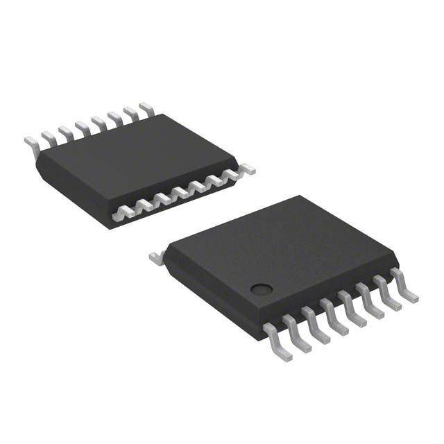
| 描述 | IC 8-BIT SHFT REG W/OUT 16-TSSOP计数器移位寄存器 8-Bit Shift Register w/Output Registers |
| 产品分类 | |
| 品牌 | Texas Instruments |
| 产品手册 | |
| 产品图片 |
|
| rohs | 符合RoHS库存产品核实请求 / 库存产品核实请求 |
| 产品系列 | 逻辑集成电路,计数器移位寄存器,Texas Instruments SN74LV594APWR74LV |
| 数据手册 | |
| 产品型号 | SN74LV594APWR |
| 产品目录页面 | |
| 产品种类 | 计数器移位寄存器 |
| 传播延迟时间 | 16.1 ns, 12.5 ns, 9.2 ns |
| 供应商器件封装 | 16-TSSOP |
| 元件数 | 1 |
| 其它名称 | 296-3842-6 |
| 功能 | 串行至并行 |
| 包装 | Digi-Reel® |
| 单位重量 | 62 mg |
| 商标 | Texas Instruments |
| 安装类型 | 表面贴装 |
| 安装风格 | SMD/SMT |
| 封装 | Reel |
| 封装/外壳 | 16-TSSOP(0.173",4.40mm 宽) |
| 封装/箱体 | TSSOP-16 |
| 工作温度 | -40°C ~ 85°C |
| 工作电源电压 | 2 V to 5.5 V |
| 工厂包装数量 | 2000 |
| 最大工作温度 | + 85 C |
| 最小工作温度 | - 40 C |
| 标准包装 | 1 |
| 每元件位数 | 8 |
| 电压-电源 | 2 V ~ 5.5 V |
| 电源电压-最大 | 5.5 V |
| 电路数量 | 8 |
| 系列 | SN74LV594A |
| 计数顺序 | Serial to Serial/Parallel |
| 输入线路数量 | 5 / 8 |
| 输出类型 | 标准 |
| 输出线路数量 | 8 |
| 逻辑类型 | 移位寄存器 |
| 逻辑系列 | 74LV |


- 商务部:美国ITC正式对集成电路等产品启动337调查
- 曝三星4nm工艺存在良率问题 高通将骁龙8 Gen1或转产台积电
- 太阳诱电将投资9.5亿元在常州建新厂生产MLCC 预计2023年完工
- 英特尔发布欧洲新工厂建设计划 深化IDM 2.0 战略
- 台积电先进制程称霸业界 有大客户加持明年业绩稳了
- 达到5530亿美元!SIA预计今年全球半导体销售额将创下新高
- 英特尔拟将自动驾驶子公司Mobileye上市 估值或超500亿美元
- 三星加码芯片和SET,合并消费电子和移动部门,撤换高东真等 CEO
- 三星电子宣布重大人事变动 还合并消费电子和移动部门
- 海关总署:前11个月进口集成电路产品价值2.52万亿元 增长14.8%


PDF Datasheet 数据手册内容提取
Product Sample & Technical Tools & Support & Folder Buy Documents Software Community SN54LV594A,SN74LV594A SCLS413J–APRIL2005–REVISEDMARCH2015 SNx4LV594A 8-Bit Shift Registers With Output Registers 1 Features 3 Description • 2-Vto5.5-VV Operation The SN74LV594A devices are 8-bit shift registers 1 CC designedfor2-Vto5.5-VV operation. • Maximumtpdof6.5nsat5V CC • TypicalVOLP (OutputGroundBounce) <0.8Vat DeviceInformation(1) V =3.3V,TA=25°C CC PARTNUMBER PACKAGE BODYSIZE(NOM) • SupportMixed-ModeVoltageOperationonAll SSOP(16) 6.20mm×5.30mm Ports SN74LV594A SOIC(16) 9.90mm×3.91mm • 8-BitSerial-In,Parallel-OutShiftRegistersWith TSSOP(16) 5.00mm×4.40mm Storage (1) For all available packages, see the orderable addendum at • IndependentDirectOverridingClearsonShiftand theendofthedatasheet. StorageRegisters LogicDiagram(PositiveLogic) • IndependentClocksforShiftandStorage Registers • Latch-upPerformanceExceeds100mAPer JESD78,ClassII • ESDProtectionExceedsJESD22 – 2000-VHuman-BodyModel(A114-A) – 1000-VCharged-DeviceModel(C101) 2 Applications • ECGElectrocardiograms • StorageServers • EPOS,ECR,andCashDrawers • ServersandHigh-PerformanceComputing 1 An IMPORTANT NOTICE at the end of this data sheet addresses availability, warranty, changes, use in safety-critical applications, intellectualpropertymattersandotherimportantdisclaimers.PRODUCTIONDATA.
SN54LV594A,SN74LV594A SCLS413J–APRIL2005–REVISEDMARCH2015 www.ti.com Table of Contents 1 Features.................................................................. 1 7 ParameterMeasurementInformation................11 2 Applications........................................................... 1 8 DetailedDescription............................................ 12 3 Description............................................................. 1 8.1 Overview.................................................................12 4 RevisionHistory..................................................... 2 8.2 FunctionalBlockDiagram.......................................13 5 PinConfigurationandFunctions......................... 3 8.3 FeatureDescription.................................................14 8.4 DeviceFunctionalModes........................................14 6 Specifications......................................................... 4 9 ApplicationandImplementation........................ 15 6.1 AbsoluteMaximumRatings......................................4 6.2 ESDRatings..............................................................4 9.1 ApplicationInformation............................................15 6.3 RecommendedOperatingConditions.......................5 9.2 TypicalApplication .................................................15 6.4 ThermalInformation..................................................5 10 PowerSupplyRecommendations..................... 17 6.5 ElectricalCharacteristics...........................................6 11 Layout................................................................... 17 6.6 SwitchingCharacteristics:V =2.5V±0.2V........6 11.1 LayoutGuidelines.................................................17 CC 6.7 SwitchingCharacteristics:V =3.3V±0.3V........7 11.2 LayoutExample....................................................17 CC 6.8 SwitchingCharacteristics:V =5V±0.5V...........7 12 DeviceandDocumentationSupport................. 18 CC 6.9 TimingRequirements:V =2.5V±0.2V..............8 12.1 Trademarks...........................................................18 CC 6.10 TimingRequirements:V =3.3V±0.3V............8 12.2 ElectrostaticDischargeCaution............................18 CC 6.11 TimingRequirements:V =5V±0.5V...............9 12.3 Glossary................................................................18 CC 6.12 NoiseCharacteristics..............................................9 13 Mechanical,Packaging,andOrderable 6.13 OperatingCharacteristics........................................9 Information........................................................... 18 6.14 TypicalCharacteristics..........................................10 4 Revision History NOTE:Pagenumbersforpreviousrevisionsmaydifferfrompagenumbersinthecurrentversion. ChangesfromRevisionI(April2005)toRevisionJ Page • AddedPinConfigurationandFunctionssection,ESDRatingstable,FeatureDescriptionsection,DeviceFunctional Modes,ApplicationandImplementationsection,PowerSupplyRecommendationssection,Layoutsection,Device andDocumentationSupportsection,andMechanical,Packaging,andOrderableInformationsection .............................. 1 2 SubmitDocumentationFeedback Copyright©2005–2015,TexasInstrumentsIncorporated SN74LV594A
SN54LV594A,SN74LV594A www.ti.com SCLS413J–APRIL2005–REVISEDMARCH2015 5 Pin Configuration and Functions D,DB,orPWPackage 16-PinSOIC,SSOP,orTSSOP TopView PinFunctions PIN I/O DESCRIPTION NO. NAME 1 Q O OutputB B 2 Q O OutputC C 3 Q O OutputD D 4 Q O OutputE E 5 Q O OutputF F 6 Q O OutputG G 7 Q O OutputH H 8 GND – Groundpin 9 Q O Q inverted H' H 10 SRCLR I Serialclear 11 SRCLK I Serialclock 12 RCLK I Storageclock 13 RCLR I Storageclear 14 SER I Serialinput 15 Q O OutputA A 16 Vcc – Powerpin Copyright©2005–2015,TexasInstrumentsIncorporated SubmitDocumentationFeedback 3 SN74LV594A
SN54LV594A,SN74LV594A SCLS413J–APRIL2005–REVISEDMARCH2015 www.ti.com 6 Specifications 6.1 Absolute Maximum Ratings overoperatingfree-airtemperaturerange(unlessotherwisenoted) (1) MIN MAX UNIT V Supplyvoltage −0.5 7 V CC V Inputvoltage(2) −0.5 7 V I V Voltagerangeappliedtoanyoutputinthehigh-impedanceorpower-offstate(2) −0.5 7 V O V Outputvoltage(2)(3) −0.5 V +0.5 V O CC I Inputclampcurrent V <0 −20 mA IK I I Outputclampcurrent V <0 −50 mA OK O I Continuousoutputcurrent V =0toV −25 25 mA O O CC T Storagetemperature −65 150 °C stg (1) StressesbeyondthoselistedunderAbsoluteMaximumRatingsmaycausepermanentdamagetothedevice.Thesearestressratings only,whichdonotimplyfunctionaloperationofthedeviceattheseoranyotherconditionsbeyondthoseindicatedunderRecommended OperatingConditions.Exposuretoabsolute-maximum-ratedconditionsforextendedperiodsmayaffectdevicereliability. (2) Theinputandoutputnegative-voltageratingsmaybeexceedediftheinputandoutputcurrentratingsareobserved. (3) Thevalueislimitedto5.5Vmaximum. 6.2 ESD Ratings VALUE UNIT Humanbodymodel(HBM),perANSI/ESDA/JEDECJS-001(1) 2000 V(ESD) Electrostaticdischarge Charged-devicemodel(CDM),perJEDECspecificationJESD22- 1000 V C101(2) (1) JEDECdocumentJEP155statesthat500-VHBMallowssafemanufacturingwithastandardESDcontrolprocess. (2) JEDECdocumentJEP157statesthat250-VCDMallowssafemanufacturingwithastandardESDcontrolprocess. 4 SubmitDocumentationFeedback Copyright©2005–2015,TexasInstrumentsIncorporated SN74LV594A
SN54LV594A,SN74LV594A www.ti.com SCLS413J–APRIL2005–REVISEDMARCH2015 6.3 Recommended Operating Conditions overoperatingfree-airtemperaturerange(unlessotherwisenoted)(1) SN54LV594A(2) SN74LV594A UNIT MIN MAX MIN MAX V Supplyvoltage 2 5.5 2 5.5 V CC V =2V 1.5 1.5 CC V =2.3Vto2.7V V ×0.7 V ×0.7 CC CC CC V High-levelinputvoltage V IH V =3Vto3.6V V ×0.7 V ×0.7 CC CC CC V =4.5Vto5.5V V ×0.7 V ×0.7 CC CC CC V =2V 0.5 0.5 CC V =2.3Vto2.7V V ×0.3 V ×0.3 CC CC CC V Low-levelinputvoltage V IL V =3Vto3.6V V ×0.3 V ×0.3 CC CC CC V =4.5Vto5.5V V ×0.3 V ×0.3 CC CC CC V Inputvoltage 0 5.5 0 5.5 V I V Outputvoltage 0 V 0 V V O CC CC V =2V –50 –50 µA CC V =2.3Vto2.7V –2 –2 CC I High-levelinputcurrent OH V =3Vto3.6V 6 6 mA CC V =4.5Vto5.5V –12 –12 CC V =2V 50 50 µA CC V =2.3Vto2.7V 2 2 CC I Low-leveloutputcurrent OL V =3Vto3.6V 6 6 mA CC V =4.5Vto5.5V 12 12 CC 200 200 InputtransitionriseorfallrateV =2.3Vto2.7VV =3Vto3.6V Δt/Δv CC CC 100 100 ns/V V =4.5Vto5.5V CC 20 20 T Operatingfree-airtemperature –55 125 –40 125 °C A (1) AllunusedinputsofthedevicemustbeheldatV orGNDtoensureproperdeviceoperation.RefertotheTIapplicationreport CC ImplicationsofSloworFloatingCMOSInputs,SCBA004. (2) ProductPreview 6.4 Thermal Information SN74LV594A THERMALMETRIC(1) D(SOIC) DB(SSOP) PW(TSSOP) UNIT 16PINS 16PINS 16PINS R Junction-to-ambientthermalresistance 80.2 97.8 106.1 θJA R Junction-to-case(top)thermalresistance 40.3 48.1 40.8 θJC(top) R Junction-to-boardthermalresistance 38 48.5 51.1 °C/W θJB ψ Junction-to-topcharacterizationparameter 9 10 3.8 JT ψ Junction-to-boardcharacterizationparameter 37.7 47.9 50.6 JB (1) Formoreinformationabouttraditionalandnewthermalmetrics,seetheICPackageThermalMetricsapplicationreport,SPRA953. Copyright©2005–2015,TexasInstrumentsIncorporated SubmitDocumentationFeedback 5 SN74LV594A
SN54LV594A,SN74LV594A SCLS413J–APRIL2005–REVISEDMARCH2015 www.ti.com 6.5 Electrical Characteristics overoperatingfree-airtemperaturerange(unlessotherwisenoted) SN74LV594A SN74LV594A PARAMETER TEST VCC SN54LV594A –40°CTO85°C –40°CTO125°C UNIT CONDITIONS MIN TYP MAX MIN TYP MAX MIN TYP MAX IOH=–50µA 2Vto5.5V VCC–0.1 VCC–0.1 VCC–0.1 IOH=–2µA 2.3V 2 2 2 VOH V IOH=–6µA 3V 2.48 2.48 2.48 IOH=–12µA 4.5V 3.8 3.8 3.8 IOH=–50µA 2Vto5.5V 0.1 0.1 0.1 IOH=–2µA 2.3V 0.4 0.4 0.4 VOL V IOH=–6µA 3V 0.44 0.44 0.44 IOH=–12µA 4.5V 0.55 0.55 0.55 II VGIN=D5.5Vor 0to5.5V ±1 ±1 ±1 µA ICC VGIN=DV,CIOC=of0 5.5V 20 20 20 µA Ioff VtoI5o.r5VVO=0 0 5 5 5 µA Ci VGIN=DVCCor 3.3V 3.5 3.5 pF 6.6 Switching Characteristics: V = 2.5 V ± 0.2 V CC overrecommendedoperatingfree-airtemperaturerange,V =2.5V±0.2V(unlessotherwisenoted).SeeFigure1. CC SN74LV594A SN74LV594A PARAMETER FROM TO LOAD TA=25°C SN54lv594A –40°CTO85°C –40°CTO125°C UNIT (INPUT) (OUTPUT) CAPACITANCE MIN TYP MAX MIN MAX MIN MAX MIN MAX CL=15pF 65(1) 80(1) 45(1) 45 35 fmax MHz CL=50pF 60 70 40 40 30 tPLH 6.4(1) 10.6(1) 1(1) 11.1(1) 1 11.1 1 12.5 tPHL SRCLK QA–QH 6.3(1) 10.4(1) 1(1) 11.1(1) 1 11.1 1 12.5 tPLH 7.4(1) 12.1(1) 1(1) 12.8(1) 1 12.8 1 15 tPHL QH’ CL=15pF 7.2(1) 11.6(1) 1(1) 12.8(1) 1 12.8 1 15 ns RCLK QA–QH 7.9(1) 12.7(1) 1(1) 13.6(1) 1 13.6 1 15.5 tPHL QH’ 7.4(1) 11.9(1) 1(1) 13.1(1) 1 13.1 1 15.5 tPLH 9.5 14.1 1 14.6 1 14.6 1 17 QA–QH tPHL SRCLR 10.8 15.5 1 17.2 1 17.2 1 19.5 tPLH 10.6 15.7 1 16.5 1 16.5 1 18.5 QH’ CL=50pF ns tPHL 11.3 16.1 1 18.6 1 18.6 1 20.5 RCLR QA–QH 12.1 17.4 1 19 1 19 1 21 tPHL QH’ 11.6 16.5 1 18.6 1 18.6 1 20.6 (1) OnproductscomplianttoMIL-PRF-38535,thisparameterisnotproductiontested. 6 SubmitDocumentationFeedback Copyright©2005–2015,TexasInstrumentsIncorporated SN74LV594A
SN54LV594A,SN74LV594A www.ti.com SCLS413J–APRIL2005–REVISEDMARCH2015 6.7 Switching Characteristics: V = 3.3 V ± 0.3 V CC overrecommendedoperatingfree-airtemperaturerange,V =3.3V±0.3V(unlessotherwisenoted).SeeFigure1. CC SN74LV594A SN74LV594A PARAMETER FROM TO LOAD TA=25°C SN54LV594A –40°CTO85°C –40°CTO125°C UNIT (INPUT) (OUTPUT) CAPACITANCE MIN TYP MAX MIN MAX MIN MAX MIN MAX CL=15pF 80(1) 120(1) 70(1) 70 60 fmax MHz CL=50pF 55 105 50 50 40 tPLH 4.6(1) 8(1) 1(1) 8.5(1) 1 8.5 1 10.5 tPHL SRCLK QA–QH 4.9(1) 8.2(1) 1(1) 8.8(1) 1 8.8 1 10.5 tPLH 5.4(1) 9.1(1) 1(1) 9.7(1) 1 9.7 1 11.5 tPHL QH’ CL=15pF 5.5(1) 9.2(1) 1(1) 9.9(1) 1 9.9 1 11.6 ns RCLK QA–QH 6(1) 9.8(1) 1(1) 10.6(1) 1 10.6 1 12.1 tPHL QH’ 5.6(1) 9.2(1) 1(1) 10(1) 1 10 1 12 tPLH 1 11.1 1 11.1 1 12.5 QA–QH tPHL SRCLR 1 13.1 1 13.1 1 15 tPLH 1 12.4 1 12.4 1 14 QH’ CL=50pF ns tPHL 1 13.9 1 13.9 1 15.5 RCLR QA–QH 1 14.4 1 14.4 1 16.1 tPHL QH’ 1 14 1 14 1 16 (1) OnproductscomplianttoMIL-PRF-38535,thisparameterisnotproductiontested. 6.8 Switching Characteristics: V = 5 V ± 0.5 V CC overrecommendedoperatingfree-airtemperaturerange,V =5V±0.5V(unlessotherwisenoted).SeeFigure1. CC SN74LV594A SN74LV594A PARAMETER FROM TO LOAD TA=25°C SN54LV594A –40°CTO85°C –40°CTO125°C UNIT (INPUT) (OUTPUT) CAPACITANCE MIN TYP MAX MIN MAX MIN MAX CL=15pF 135(1) 170(1) 115(1) 115 105 fmax MHz CL=50pF 120 140 95 95 85 tPLH 3.3(1) 6.2(1) 1(1) 6.5(1) 1 6.5 1 8 tPHL SRCLK QA–QH 3.7(1) 6.5(1) 1(1) 6.9(1) 1 6.9 1 8.5 tPLH 3.7(1) 6.8(1) 1(1) 7.2(1) 1 7.2 1 8.5 tPHL QH’ CL=15pF 4.1(1) 7.2(1) 1(1) 7.6(1) 1 7.6 1 9 ns RCLK QA–QH 4.5(1) 7.6(1) 1(1) 8.2(1) 1 8.2 1 9.5 tPHL QH’ 4.1(1) 7.1(1) 1(1) 7.6(1) 1 7.6 1 9 tPLH 4.9 7.8 1 8.3 1 8.3 1 9.6 QA–QH tPHL SRCLR 5.8 8.9 1 9.7 1 9.7 1 11 tPLH 5.5 8.6 1 9.1 1 9.1 1 10.5 QH’ CL=50pF ns tPHL 6 9.2 1 10.1 1 10.1 1 11.5 RCLR QA–QH 6.6 10 1 10.7 1 10.7 1 12 tPHL QH’ 6 9.2 1 10.1 1 10.1 1 11.5 (1) OnproductscomplianttoMIL-PRF-38535,thisparameterisnotproductiontested. Copyright©2005–2015,TexasInstrumentsIncorporated SubmitDocumentationFeedback 7 SN74LV594A
SN54LV594A,SN74LV594A SCLS413J–APRIL2005–REVISEDMARCH2015 www.ti.com 6.9 Timing Requirements: V = 2.5 V ± 0.2 V CC overrecommendedoperatingfree-airtemperaturerange,V =2.5V±0.2V.SeeFigure1. CC SN74LV594A SN74LV594A TA=25°C SN54LV594A –40°CTO85°C –40°CTO125°C UNIT MIN MAX MIN MAX MIN MAX MIN MAX RCLKorSRCLKhighorlow 7 7.5 7.5 8.5 tw Pulseduration ns RCKRorSCRCLRlow 6 6.5 6.5 7.5 SERbeforeSRCLK↑ 5.5 5.5 5.5 6 SRCLK↑beforeRCLK↑ 8 9 9 10 SCRCLRlowbeforeRCLK↑(1) 8.5 9.5 9.5 10.5 tsu Setuptime ns SRCLRhigh(inactive)before 6 6.8 6.8 7.5 SRCLK↑ RCLKhigh(inactive)beforeRCLK↑ 6.7 7.6 7.6 8.5 th Holdtime SERafterSRCLK↑ 1.5 1.5 1.5 2 ns (1) Thissetuptimeallowsthestorageregistertoreceivestabledatafromtheshiftregister.Theclockscanbetiedtogether,inwhichcase theshiftregisterisoneclockpulseaheadofthestorageregister. 6.10 Timing Requirements: V = 3.3 V ± 0.3 V CC overrecommendedoperatingfree-airtemperaturerange,V =3.3V±0.3V.SeeFigure1. CC SN74LV594A SN74LV594A TA=25°C SN54LV594A –40°CTO85°C –40°CTO125°C UNIT MIN MAX MIN MAX MIN MAX MIN MAX RCLKorSRCLKhighorlow 5.5 5.5 5.5 6.5 tw Pulseduration ns RCKRorSCRCLRlow 5 5 5 6 SERbeforeSRCLK↑ 3.5 3.5 3.5 4 SRCLK↑beforeRCLK↑ 8 8.5 8.5 9.5 SCRCLRlowbeforeRCLK↑(1) 8 9 9 10 tsu Setuptime ns SRCLRhigh(inactive)before 4.2 4.8 4.8 5.5 SRCLK↑ RCLKhigh(inactive)beforeRCLK↑ 4.6 5.3 5.3 6 th Holdtime SERafterSRCLK↑ 1.5 1.5 1.5 2 ns (1) Thissetuptimeallowsthestorageregistertoreceivestabledatafromtheshiftregister.Theclockscanbetiedtogether,inwhichcase theshiftregisterisoneclockpulseaheadofthestorageregister. 8 SubmitDocumentationFeedback Copyright©2005–2015,TexasInstrumentsIncorporated SN74LV594A
SN54LV594A,SN74LV594A www.ti.com SCLS413J–APRIL2005–REVISEDMARCH2015 6.11 Timing Requirements: V = 5 V ± 0.5 V CC overrecommendedoperatingfree-airtemperaturerange,V =2.5V±0.2V.SeeFigure1. CC SN74LV594A SN74LV594A TA=25°C SN54LV594A –40°CTO85°C –40°CTO125°C UNIT MIN MAX MIN MAX MIN MAX MIN MAX RCLKorSRCLKhighorlow 5 5 5 6 tw Pulseduration ns RCKRorSCRCLRlow 5.2 5.2 5.2 6.2 SERbeforeSRCLK↑ 3 3 3 3.5 SRCLK↑beforeRCLK↑ 5 5 5 6 SCRCLRlowbeforeRCLK↑(1) 5 5 5 5.5 tsu Setuptime ns SRCLRhigh(inactive)before 2.9 3.3 3.3 4 SRCLK↑ RCLKhigh(inactive)beforeRCLK↑ 3.2 3.7 3.7 4.5 th Holdtime SERafterSRCLK↑ 2 2 2 2.5 ns (1) Thissetuptimeallowsthestorageregistertoreceivestabledatafromtheshiftregister.Theclockscanbetiedtogether,inwhichcase theshiftregisterisoneclockpulseaheadofthestorageregister. 6.12 Noise Characteristics(1) overoperatingfree-airtemperaturerange(unlessotherwisenoted),V =3.3V,C =50pF,T =25°C CC L A PARAMETER MIN TYP MAX UNIT V Quietoutput,maximumdynamicV 0.5 0.8 V OL(P) OL V Quietoutput,minimumdynamicV –0.1 –0.8 V OL(V) OL V Quietoutput,minimumdynamicV 2.8 V OH(V) OH V High-leveldynamicinputvoltage 2.31 V IH(V) V Low-leveldynamicinputvoltage 0.99 V IL(V) (1) Characteristicsareforsurface-mountpackagesonly. 6.13 Operating Characteristics T =25°C A PARAMETER TESTCONDITIONS V TYP UNIT CC 3.3V 93 C Powerdissipationcapacitance f=10MHz pF pd 5V 112 Copyright©2005–2015,TexasInstrumentsIncorporated SubmitDocumentationFeedback 9 SN74LV594A
SN54LV594A,SN74LV594A SCLS413J–APRIL2005–REVISEDMARCH2015 www.ti.com Figure1. TimingDiagram 6.14 Typical Characteristics 6 7 6 5 5 4 s) s) 4 n n D ( 3 D ( P P 3 T T 2 2 1 1 0 0 -100 -50 0 50 100 150 0 1 2 3 4 5 6 Temperature Vcc D001 D002 Figure2.TPDvs.Temperatureat3.3V Figure3.TPDvs.Vccat25°C 10 SubmitDocumentationFeedback Copyright©2005–2015,TexasInstrumentsIncorporated SN74LV594A
SN54LV594A,SN74LV594A www.ti.com SCLS413J–APRIL2005–REVISEDMARCH2015 7 Parameter Measurement Information Figure4. LoadCircuitandVoltageWaveforms Copyright©2005–2015,TexasInstrumentsIncorporated SubmitDocumentationFeedback 11 SN74LV594A
SN54LV594A,SN74LV594A SCLS413J–APRIL2005–REVISEDMARCH2015 www.ti.com 8 Detailed Description 8.1 Overview TheSN74LV594Adevicesare8-bitshiftregistersdesignedfor2-Vto5.5-VV operation. CC These devices contain an 8-bit serial-in, parallel-out shift register that feeds an 8-bit D-type storage register. Separateclocks(RCLK,SRCLK)anddirectoverridingclear(RCLR,SRCLR)inputsareprovidedontheshiftand storage registers. A serial output (Q ) is provided for cascading purposes. The shift-register (SRCLK) and H′ storage-register (RCLK) clocks are positive-edge triggered. If the clocks are tied together, the shift register alwaysisoneclockpulseaheadofthestorageregister. 12 SubmitDocumentationFeedback Copyright©2005–2015,TexasInstrumentsIncorporated SN74LV594A
SN54LV594A,SN74LV594A www.ti.com SCLS413J–APRIL2005–REVISEDMARCH2015 8.2 Functional Block Diagram Figure5. LogicDiagram(PositiveLogic) Copyright©2005–2015,TexasInstrumentsIncorporated SubmitDocumentationFeedback 13 SN74LV594A
SN54LV594A,SN74LV594A SCLS413J–APRIL2005–REVISEDMARCH2015 www.ti.com 8.3 Feature Description The device’s wide operating range allows it to be used in a variety of systems that use different logic levels. The low propagation delay allows fast switching and higher speeds of operation. In addition, the low ground bounce stabilizestheperformanceofnon-switchingoutputswhileanotheroutputisswitching. 8.4 Device Functional Modes Table1.FunctionTable INPUTS FUNCTION SER SRCLK SRCLR RCLK RCLR X X L X X Shiftregisteriscleared. Firststageofshiftregistergoeslow.Otherstages L ↑ H X X storethedataofpreviousstage,repectively. Firststageofshiftregistergoeshigh.Otherstages H ↑ H X X storethedataofpreviousstage,respectively. L ↓ H X X Shiftregisterstateisnotchanged. X X X X L Storageregisteriscleared. X X X ↑ H Shiftregisterdataisstoredinthestorageregister. X X X ↓ H Storageregisterstateisnotchanged. 14 SubmitDocumentationFeedback Copyright©2005–2015,TexasInstrumentsIncorporated SN74LV594A
SN54LV594A,SN74LV594A www.ti.com SCLS413J–APRIL2005–REVISEDMARCH2015 9 Application and Implementation NOTE Information in the following applications sections is not part of the TI component specification, and TI does not warrant its accuracy or completeness. TI’s customers are responsible for determining suitability of components for their purposes. Customers should validateandtesttheirdesignimplementationtoconfirmsystemfunctionality. 9.1 Application Information The SN74LV594A is a low drive CMOS device that can be used for a multitude of bus interface type applications where output ringing is a concern. The low drive and slow edge rates will minimize overshoot and undershoot on theoutputs. 9.2 Typical Application Figure6. TypicalApplicationSchematic 9.2.1 DesignRequirements ThisdeviceusesCMOStechnologyandhasbalancedoutputdrive.Takecaretoavoidbuscontentionbecauseit can drive currents that would exceed maximum limits. The high drive will also create fast edges into light loads soconsiderroutingandloadconditionstopreventringing. Copyright©2005–2015,TexasInstrumentsIncorporated SubmitDocumentationFeedback 15 SN74LV594A
SN54LV594A,SN74LV594A SCLS413J–APRIL2005–REVISEDMARCH2015 www.ti.com Typical Application (continued) 9.2.2 DetailedDesignProcedure • Recommendedinputconditions: – Risetimeandfalltimespecs.See(Δt/ΔV)inRecommendedOperatingConditions. – Specifiedhighandlowlevels.See(V andV )inRecommendedOperatingConditions. IH IL – Inputsareovervoltagetolerantallowingthemtogoashighas5.5VatanyvalidV . CC • Recommendedoutputconditions: – Loadcurrentsshouldnotexceed25mAperoutputand50mAtotalforthepart. – OutputsshouldnotbepulledaboveV . CC 9.2.3 ApplicationCurves Figure7. SwitchingCharacteristicsComparison 16 SubmitDocumentationFeedback Copyright©2005–2015,TexasInstrumentsIncorporated SN74LV594A
SN54LV594A,SN74LV594A www.ti.com SCLS413J–APRIL2005–REVISEDMARCH2015 10 Power Supply Recommendations The power supply can be any voltage between the minimum and maximum supply voltage rating located in the Recommended Operating Conditions. Each V terminal should have a good bypass capacitor to prevent power CC disturbance. For devices with a single supply, TI recommends a 0.1-μF capacitor and if there are multiple V CC terminals then TI recommends a 0.01-μF or 0.022-μF capacitor for each power terminal. Multiple bypass capacitors can be paralleled to reject different frequencies of noise. Frequencies of 0.1 μF and 1 μF are commonly used in parallel. The bypass capacitor should be installed as close as possible to the power terminal forbestresults. 11 Layout 11.1 Layout Guidelines Whenusingmultiplebitlogicdevicesinputsshouldnoteverfloat. In many cases, functions or parts of functions of digital logic devices are unused, for example, when only two inputs of a triple-input AND gate are used or only three of the four buffer gates are used. Such input pins should not be left unconnected because the undefined voltages at the outside connections result in undefined operational states. Specified below are the rules that must be observed under all circumstances. All unused inputs of digital logic devices must be connected to a high or low bias to prevent them from floating. The logic level that should be applied to any particular unused input depends on the function of the device. Generally they will be tied to GND or V whichever make more sense or is more convenient. Floating outputs is generally CC acceptable, unless the part is a transceiver. If the transceiver has an output enable pin it will disable the outputs section of the part when asserted. This will not disable the input section of the I.O’s so they also cannot float whendisabled. 11.2 Layout Example Figure8. LayoutExample Copyright©2005–2015,TexasInstrumentsIncorporated SubmitDocumentationFeedback 17 SN74LV594A
SN54LV594A,SN74LV594A SCLS413J–APRIL2005–REVISEDMARCH2015 www.ti.com 12 Device and Documentation Support 12.1 Trademarks Alltrademarksarethepropertyoftheirrespectiveowners. 12.2 Electrostatic Discharge Caution Thesedeviceshavelimitedbuilt-inESDprotection.Theleadsshouldbeshortedtogetherorthedeviceplacedinconductivefoam duringstorageorhandlingtopreventelectrostaticdamagetotheMOSgates. 12.3 Glossary SLYZ022—TIGlossary. Thisglossarylistsandexplainsterms,acronyms,anddefinitions. 13 Mechanical, Packaging, and Orderable Information The following pages include mechanical, packaging, and orderable information. This information is the most current data available for the designated devices. This data is subject to change without notice and revision of thisdocument.Forbrowser-basedversionsofthisdatasheet,refertotheleft-handnavigation. 18 SubmitDocumentationFeedback Copyright©2005–2015,TexasInstrumentsIncorporated SN74LV594A
PACKAGE OPTION ADDENDUM www.ti.com 5-Mar-2015 PACKAGING INFORMATION Orderable Device Status Package Type Package Pins Package Eco Plan Lead/Ball Finish MSL Peak Temp Op Temp (°C) Device Marking Samples (1) Drawing Qty (2) (6) (3) (4/5) SN74LV594AD ACTIVE SOIC D 16 40 Green (RoHS CU NIPDAU Level-1-260C-UNLIM -40 to 125 LV594A & no Sb/Br) SN74LV594ADBR ACTIVE SSOP DB 16 2000 Green (RoHS CU NIPDAU Level-1-260C-UNLIM -40 to 125 LV594A & no Sb/Br) SN74LV594ADE4 ACTIVE SOIC D 16 40 Green (RoHS CU NIPDAU Level-1-260C-UNLIM -40 to 125 LV594A & no Sb/Br) SN74LV594ADG4 ACTIVE SOIC D 16 40 Green (RoHS CU NIPDAU Level-1-260C-UNLIM -40 to 125 LV594A & no Sb/Br) SN74LV594ADR ACTIVE SOIC D 16 2500 Green (RoHS CU NIPDAU Level-1-260C-UNLIM -40 to 125 LV594A & no Sb/Br) SN74LV594ADRG4 ACTIVE SOIC D 16 2500 Green (RoHS CU NIPDAU Level-1-260C-UNLIM -40 to 125 LV594A & no Sb/Br) SN74LV594APW ACTIVE TSSOP PW 16 90 Green (RoHS CU NIPDAU Level-1-260C-UNLIM -40 to 125 LV594A & no Sb/Br) SN74LV594APWG4 ACTIVE TSSOP PW 16 90 Green (RoHS CU NIPDAU Level-1-260C-UNLIM -40 to 125 LV594A & no Sb/Br) SN74LV594APWR ACTIVE TSSOP PW 16 2000 Green (RoHS CU NIPDAU | CU SN Level-1-260C-UNLIM -40 to 125 LV594A & no Sb/Br) SN74LV594APWRE4 ACTIVE TSSOP PW 16 2000 Green (RoHS CU NIPDAU Level-1-260C-UNLIM -40 to 125 LV594A & no Sb/Br) SN74LV594APWRG4 ACTIVE TSSOP PW 16 2000 Green (RoHS CU NIPDAU Level-1-260C-UNLIM -40 to 125 LV594A & no Sb/Br) SN74LV594APWT ACTIVE TSSOP PW 16 250 Green (RoHS CU NIPDAU Level-1-260C-UNLIM -40 to 125 LV594A & no Sb/Br) SN74LV594APWTG4 ACTIVE TSSOP PW 16 250 Green (RoHS CU NIPDAU Level-1-260C-UNLIM -40 to 125 LV594A & no Sb/Br) (1) The marketing status values are defined as follows: ACTIVE: Product device recommended for new designs. LIFEBUY: TI has announced that the device will be discontinued, and a lifetime-buy period is in effect. NRND: Not recommended for new designs. Device is in production to support existing customers, but TI does not recommend using this part in a new design. PREVIEW: Device has been announced but is not in production. Samples may or may not be available. OBSOLETE: TI has discontinued the production of the device. Addendum-Page 1
PACKAGE OPTION ADDENDUM www.ti.com 5-Mar-2015 (2) Eco Plan - The planned eco-friendly classification: Pb-Free (RoHS), Pb-Free (RoHS Exempt), or Green (RoHS & no Sb/Br) - please check http://www.ti.com/productcontent for the latest availability information and additional product content details. TBD: The Pb-Free/Green conversion plan has not been defined. Pb-Free (RoHS): TI's terms "Lead-Free" or "Pb-Free" mean semiconductor products that are compatible with the current RoHS requirements for all 6 substances, including the requirement that lead not exceed 0.1% by weight in homogeneous materials. Where designed to be soldered at high temperatures, TI Pb-Free products are suitable for use in specified lead-free processes. Pb-Free (RoHS Exempt): This component has a RoHS exemption for either 1) lead-based flip-chip solder bumps used between the die and package, or 2) lead-based die adhesive used between the die and leadframe. The component is otherwise considered Pb-Free (RoHS compatible) as defined above. Green (RoHS & no Sb/Br): TI defines "Green" to mean Pb-Free (RoHS compatible), and free of Bromine (Br) and Antimony (Sb) based flame retardants (Br or Sb do not exceed 0.1% by weight in homogeneous material) (3) MSL, Peak Temp. - The Moisture Sensitivity Level rating according to the JEDEC industry standard classifications, and peak solder temperature. (4) There may be additional marking, which relates to the logo, the lot trace code information, or the environmental category on the device. (5) Multiple Device Markings will be inside parentheses. Only one Device Marking contained in parentheses and separated by a "~" will appear on a device. If a line is indented then it is a continuation of the previous line and the two combined represent the entire Device Marking for that device. (6) Lead/Ball Finish - Orderable Devices may have multiple material finish options. Finish options are separated by a vertical ruled line. Lead/Ball Finish values may wrap to two lines if the finish value exceeds the maximum column width. Important Information and Disclaimer:The information provided on this page represents TI's knowledge and belief as of the date that it is provided. TI bases its knowledge and belief on information provided by third parties, and makes no representation or warranty as to the accuracy of such information. Efforts are underway to better integrate information from third parties. TI has taken and continues to take reasonable steps to provide representative and accurate information but may not have conducted destructive testing or chemical analysis on incoming materials and chemicals. TI and TI suppliers consider certain information to be proprietary, and thus CAS numbers and other limited information may not be available for release. In no event shall TI's liability arising out of such information exceed the total purchase price of the TI part(s) at issue in this document sold by TI to Customer on an annual basis. Addendum-Page 2
PACKAGE MATERIALS INFORMATION www.ti.com 20-Dec-2018 TAPE AND REEL INFORMATION *Alldimensionsarenominal Device Package Package Pins SPQ Reel Reel A0 B0 K0 P1 W Pin1 Type Drawing Diameter Width (mm) (mm) (mm) (mm) (mm) Quadrant (mm) W1(mm) SN74LV594ADR SOIC D 16 2500 330.0 16.4 6.5 10.3 2.1 8.0 16.0 Q1 SN74LV594APWR TSSOP PW 16 2000 330.0 12.4 6.9 5.6 1.6 8.0 12.0 Q1 SN74LV594APWR TSSOP PW 16 2000 330.0 12.4 6.9 5.6 1.6 8.0 12.0 Q1 SN74LV594APWRG4 TSSOP PW 16 2000 330.0 12.4 6.9 5.6 1.6 8.0 12.0 Q1 SN74LV594APWT TSSOP PW 16 250 330.0 12.4 6.9 5.6 1.6 8.0 12.0 Q1 PackMaterials-Page1
PACKAGE MATERIALS INFORMATION www.ti.com 20-Dec-2018 *Alldimensionsarenominal Device PackageType PackageDrawing Pins SPQ Length(mm) Width(mm) Height(mm) SN74LV594ADR SOIC D 16 2500 333.2 345.9 28.6 SN74LV594APWR TSSOP PW 16 2000 367.0 367.0 35.0 SN74LV594APWR TSSOP PW 16 2000 364.0 364.0 27.0 SN74LV594APWRG4 TSSOP PW 16 2000 367.0 367.0 35.0 SN74LV594APWT TSSOP PW 16 250 367.0 367.0 35.0 PackMaterials-Page2
MECHANICAL DATA MSSO002E – JANUARY 1995 – REVISED DECEMBER 2001 DB (R-PDSO-G**) PLASTIC SMALL-OUTLINE 28 PINS SHOWN 0,38 0,65 0,15 M 0,22 28 15 0,25 0,09 5,60 8,20 5,00 7,40 Gage Plane 1 14 0,25 A 0°–(cid:1)8° 0,95 0,55 Seating Plane 2,00 MAX 0,05 MIN 0,10 PINS ** 14 16 20 24 28 30 38 DIM A MAX 6,50 6,50 7,50 8,50 10,50 10,50 12,90 A MIN 5,90 5,90 6,90 7,90 9,90 9,90 12,30 4040065/E 12/01 NOTES: A. All linear dimensions are in millimeters. B. This drawing is subject to change without notice. C. Body dimensions do not include mold flash or protrusion not to exceed 0,15. D. Falls within JEDEC MO-150 • POST OFFICE BOX 655303 DALLAS, TEXAS 75265
None
None
PACKAGE OUTLINE PW0016A TSSOP - 1.2 mm max height SCALE 2.500 SMALL OUTLINE PACKAGE SEATING PLANE C 6.6 TYP 6.2 A 0.1 C PIN 1 INDEX AREA 14X 0.65 16 1 2X 5.1 4.55 4.9 NOTE 3 8 9 0.30 B 4.5 16X 0.19 1.2 MAX 4.3 0.1 C A B NOTE 4 (0.15) TYP SEE DETAIL A 0.25 GAGE PLANE 0.15 0.05 0.75 0.50 0 -8 DETA 20AIL A TYPICAL 4220204/A 02/2017 NOTES: 1. All linear dimensions are in millimeters. Any dimensions in parenthesis are for reference only. Dimensioning and tolerancing per ASME Y14.5M. 2. This drawing is subject to change without notice. 3. This dimension does not include mold flash, protrusions, or gate burrs. Mold flash, protrusions, or gate burrs shall not exceed 0.15 mm per side. 4. This dimension does not include interlead flash. Interlead flash shall not exceed 0.25 mm per side. 5. Reference JEDEC registration MO-153. www.ti.com
EXAMPLE BOARD LAYOUT PW0016A TSSOP - 1.2 mm max height SMALL OUTLINE PACKAGE 16X (1.5) SYMM (R0.05) TYP 1 16X (0.45) 16 SYMM 14X (0.65) 8 9 (5.8) LAND PATTERN EXAMPLE EXPOSED METAL SHOWN SCALE: 10X SOLDER MASK METAL UNDER SOLDER MASK OPENING METAL SOLDER MASK OPENING EXPOSED METAL EXPOSED METAL 0.05 MAX 0.05 MIN ALL AROUND ALL AROUND NON-SOLDER MASK SOLDER MASK DEFINED DEFINED (PREFERRED) SOLDE15.000R MASK DETAILS 4220204/A 02/2017 NOTES: (continued) 6. Publication IPC-7351 may have alternate designs. 7. Solder mask tolerances between and around signal pads can vary based on board fabrication site. www.ti.com
EXAMPLE STENCIL DESIGN PW0016A TSSOP - 1.2 mm max height SMALL OUTLINE PACKAGE 16X (1.5) SYMM (R0.05) TYP 1 16X (0.45) 16 SYMM 14X (0.65) 8 9 (5.8) SOLDER PASTE EXAMPLE BASED ON 0.125 mm THICK STENCIL SCALE: 10X 4220204/A 02/2017 NOTES: (continued) 8. Laser cutting apertures with trapezoidal walls and rounded corners may offer better paste release. IPC-7525 may have alternate design recommendations. 9. Board assembly site may have different recommendations for stencil design. www.ti.com
IMPORTANTNOTICEANDDISCLAIMER TIPROVIDESTECHNICALANDRELIABILITYDATA(INCLUDINGDATASHEETS),DESIGNRESOURCES(INCLUDINGREFERENCE DESIGNS),APPLICATIONOROTHERDESIGNADVICE,WEBTOOLS,SAFETYINFORMATION,ANDOTHERRESOURCES“ASIS” ANDWITHALLFAULTS,ANDDISCLAIMSALLWARRANTIES,EXPRESSANDIMPLIED,INCLUDINGWITHOUTLIMITATIONANY IMPLIEDWARRANTIESOFMERCHANTABILITY,FITNESSFORAPARTICULARPURPOSEORNON-INFRINGEMENTOFTHIRD PARTYINTELLECTUALPROPERTYRIGHTS. TheseresourcesareintendedforskilleddevelopersdesigningwithTIproducts.Youaresolelyresponsiblefor(1)selectingtheappropriate TIproductsforyourapplication,(2)designing,validatingandtestingyourapplication,and(3)ensuringyourapplicationmeetsapplicable standards,andanyothersafety,security,orotherrequirements.Theseresourcesaresubjecttochangewithoutnotice.TIgrantsyou permissiontousetheseresourcesonlyfordevelopmentofanapplicationthatusestheTIproductsdescribedintheresource.Other reproductionanddisplayoftheseresourcesisprohibited.NolicenseisgrantedtoanyotherTIintellectualpropertyrightortoanythird partyintellectualpropertyright.TIdisclaimsresponsibilityfor,andyouwillfullyindemnifyTIanditsrepresentativesagainst,anyclaims, damages,costs,losses,andliabilitiesarisingoutofyouruseoftheseresources. TI’sproductsareprovidedsubjecttoTI’sTermsofSale(www.ti.com/legal/termsofsale.html)orotherapplicabletermsavailableeitheron ti.comorprovidedinconjunctionwithsuchTIproducts.TI’sprovisionoftheseresourcesdoesnotexpandorotherwisealterTI’sapplicable warrantiesorwarrantydisclaimersforTIproducts. MailingAddress:TexasInstruments,PostOfficeBox655303,Dallas,Texas75265 Copyright©2018,TexasInstrumentsIncorporated