ICGOO在线商城 > 集成电路(IC) > 接口 - 模拟开关,多路复用器,多路分解器 > SN74LV4053ATDRQ1
 Datasheet下载
- 型号: SN74LV4053ATDRQ1
- 制造商: Texas Instruments
- 库位|库存: xxxx|xxxx
- 要求:
| 数量阶梯 | 香港交货 | 国内含税 |
| +xxxx | $xxxx | ¥xxxx |
查看当月历史价格
查看今年历史价格
SN74LV4053ATDRQ1产品简介:
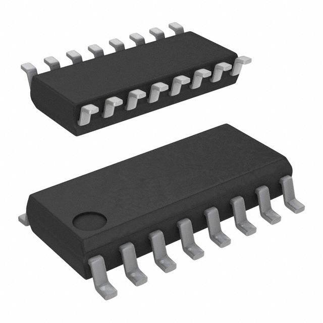
ICGOO电子元器件商城为您提供SN74LV4053ATDRQ1由Texas Instruments设计生产,在icgoo商城现货销售,并且可以通过原厂、代理商等渠道进行代购。 SN74LV4053ATDRQ1价格参考¥1.82-¥4.73。Texas InstrumentsSN74LV4053ATDRQ1封装/规格:接口 - 模拟开关,多路复用器,多路分解器, 3 Circuit IC Switch 2:1 75Ohm 16-SOIC。您可以下载SN74LV4053ATDRQ1参考资料、Datasheet数据手册功能说明书,资料中有SN74LV4053ATDRQ1 详细功能的应用电路图电压和使用方法及教程。
| 参数 | 数值 |
| 产品目录 | 集成电路 (IC)半导体 |
| 描述 | IC MUX/DEMUX TRIPLE 2X1 16SOIC多路器开关 IC Triple 2 Ch Anlg Mltplxr Demltplxr |
| 产品分类 | |
| 品牌 | Texas Instruments |
| 产品手册 | |
| 产品图片 |
|
| rohs | 符合RoHS无铅 / 符合限制有害物质指令(RoHS)规范要求 |
| 产品系列 | 开关 IC,多路器开关 IC,Texas Instruments SN74LV4053ATDRQ174LV |
| 数据手册 | |
| 产品型号 | SN74LV4053ATDRQ1 |
| 产品目录页面 | |
| 产品种类 | 多路器开关 IC |
| 传播延迟时间 | 8 ns |
| 供应商器件封装 | 16-SOIC N |
| 其它名称 | 296-24243-1 |
| 功能 | 多路复用器/多路分解器 |
| 包装 | 剪切带 (CT) |
| 单位重量 | 141.700 mg |
| 商标 | Texas Instruments |
| 安装类型 | 表面贴装 |
| 安装风格 | SMD/SMT |
| 导通电阻 | 75 欧姆 |
| 导通电阻—最大值 | 75 Ohms |
| 封装 | Reel |
| 封装/外壳 | 16-SOIC(0.154",3.90mm 宽) |
| 封装/箱体 | SOIC-16 |
| 工作温度 | -40°C ~ 105°C |
| 工作电源电压 | 2 V to 5.5 V |
| 工作电源电流 | 20 uA |
| 工厂包装数量 | 2500 |
| 带宽 | 50 Mhz |
| 开关配置 | 3 X SPDT |
| 最大工作温度 | + 105 C |
| 最小工作温度 | - 40 C |
| 标准包装 | 1 |
| 电压-电源,单/双 (±) | 2 V ~ 5.5 V |
| 电压源 | 单电源 |
| 电流-电源 | 20µA |
| 电路 | 3 x 2:1 |
| 空闲时间—最大值 | 20 ns |
| 系列 | SN74LV4053A-Q1 |
| 运行时间—最大值 | 20 ns |
| 通道数量 | 3 Channel |


- 商务部:美国ITC正式对集成电路等产品启动337调查
- 曝三星4nm工艺存在良率问题 高通将骁龙8 Gen1或转产台积电
- 太阳诱电将投资9.5亿元在常州建新厂生产MLCC 预计2023年完工
- 英特尔发布欧洲新工厂建设计划 深化IDM 2.0 战略
- 台积电先进制程称霸业界 有大客户加持明年业绩稳了
- 达到5530亿美元!SIA预计今年全球半导体销售额将创下新高
- 英特尔拟将自动驾驶子公司Mobileye上市 估值或超500亿美元
- 三星加码芯片和SET,合并消费电子和移动部门,撤换高东真等 CEO
- 三星电子宣布重大人事变动 还合并消费电子和移动部门
- 海关总署:前11个月进口集成电路产品价值2.52万亿元 增长14.8%


PDF Datasheet 数据手册内容提取
SN74LV4053A-Q1 www.ti.com SCLS521C–AUGUST2003–REVISEDJUNE2011 TRIPLE 2-CHANNEL ANALOG MULTIPLEXER/DEMULTIPLEXER CheckforSamples:SN74LV4053A-Q1 FEATURES 1 D OR PW PACKAGE • QualifiedforAutomotiveApplications (TOPVIEW) • ESDProtectionExceeds2000VPer MIL-STD-883,Method3015;Exceeds200V 2Y1 VCC UsingMachineModel(C=200pF,R=0) 2Y0 2-COM • 2-Vto5.5-VV Operation 3Y1 1-COM CC • SupportsMixed-ModeVoltageOperationon 3-COM 1Y1 AllPorts 3Y0 1Y0 • HighOn-OffOutput-VoltageRatio INH A • LowCrosstalkBetweenSwitches GND B • IndividualSwitchControls GND C • ExtremelyLowInputCurrent DESCRIPTION Thistriple2-channelCMOSanalogmultiplexer/demultiplexerisdesignedfor2-Vto5.5-VV operation. CC The SN74LV4053A handles both analog and digital signals. Each channel permits signals with amplitudes up to 5.5V(peak)tobetransmittedineitherdirection. Applications include signal gating, chopping, modulation or demodulation (modem), and signal multiplexing for analog-to-digitalanddigital-to-analogconversionsystems. ORDERINGINFORMATION(1) T PACKAGE(2) ORDERABLEPARTNUMBER TOP-SIDEMARKING A SOIC−D Tapeandreel SN74LV4053ATDRQ1 L4053AQ –40°Cto105°C TSSOP–PW Tapeandreel SN74LV4053ATPWRQ1 L4053AQ –40°Cto125°C TSSOP–PW Tapeandreel SN74LV4053AQPWRQ1 4053AQ1 (1) Forthemostcurrentpackageandorderinginformation,seethePackageOptionAddendumattheendofthisdocument,orseetheTI websiteatwww.ti.com. (2) Packagedrawings,thermaldata,andsymbolizationareavailableatwww.ti.com/packaging. FUNCTIONTABLE INPUTS ON INH C B A CHANNEL L L L L 1Y0,2Y0,3Y0 L L L H 1Y1,2Y0,3Y0 L L H L 1Y0,2Y1,3Y0 L L H H 1Y1,2Y1,3Y0 L H L L 1Y0,2Y0,3Y1 L H L H 1Y1,2Y0,3Y1 L H H L 1Y0,2Y1,3Y1 L H H H 1Y1,2Y1,3Y1 H X X X None 1 Pleasebeawarethatanimportantnoticeconcerningavailability,standardwarranty,anduseincriticalapplicationsofTexas Instrumentssemiconductorproductsanddisclaimerstheretoappearsattheendofthisdatasheet. PRODUCTIONDATAinformationiscurrentasofpublicationdate. Copyright©2003–2011,TexasInstrumentsIncorporated Products conform to specifications per the terms of the Texas Instruments standard warranty. Production processing does not necessarilyincludetestingofallparameters.
SN74LV4053A-Q1 SCLS521C–AUGUST2003–REVISEDJUNE2011 www.ti.com LOGICDIAGRAM(POSITIVELOGIC) 15 2-COM 14 1-COM 12 1Y0 13 1Y1 2 2Y0 1 2Y1 5 3Y0 3 3Y1 4 3-COM 2 Copyright©2003–2011,TexasInstrumentsIncorporated
SN74LV4053A-Q1 www.ti.com SCLS521C–AUGUST2003–REVISEDJUNE2011 ABSOLUTE MAXIMUM RATINGS(1) overoperatingfree-airtemperaturerange(unlessotherwisenoted) V Supplyvoltagerange –0.5Vto7V CC V Inputvoltagerange(2) –0.5Vto7V I V SwitchI/Ovoltagerange(2) (3) –0.5VtoV +0.5V IO CC I Inputclampcurrent V <0 –20mA IK I I I/Odiodecurrent V <0 –50mA IOK IO I Switchthroughcurrent V =0toV ±25mA T IO CC ContinuouscurrentthroughV orGND ±50mA CC Dpackage 73°C/W θ Packagethermalimpedance(4) JA PWpackage 108°C/W T Storagetemperaturerange –65°Cto150°C stg (1) Stressesbeyondthoselistedunderabsolutemaximumratingsmaycausepermanentdamagetothedevice.Thesearestressratings only,andfunctionaloperationofthedeviceattheseoranyotherconditionsbeyondthoseindicatedunderrecommendedoperating conditionsisnotimplied.Exposuretoabsolute-maximum-ratedconditionsforextendedperiodsmayaffectdevicereliability. (2) Theinputandoutputnegative-voltageratingsmaybeexceedediftheinputandoutputcurrentratingsareobserved. (3) Thisvalueislimitedto5.5Vmaximum. (4) ThepackagethermalimpedanceiscalculatedinaccordancewithJESD51-7. RECOMMENDED OPERATING CONDITIONS(1) MIN MAX UNIT V Supplyvoltage 2(2) 5.5 V CC V =2V 1.5 CC High-levelinputvoltage, VCC=2.3Vto2.7V VCC×0.7 V V IH controlinputs V =3Vto3.6V V ×0.7 CC CC V =4.5Vto5.5V V ×0.7 CC CC V =2V 0.5 CC Low-levelinputvoltage, VCC=2.3Vto2.7V VCC×0.3 V V IL controlinputs V =3Vto3.6V V ×0.3 CC CC V =4.5Vto5.5V V ×0.3 CC CC V Controlinputvoltage 0 5.5 V I V Input/outputvoltage 0 V V IO CC V =2.3Vto2.7V 200 CC Δt/Δv Inputtransitionriseorfallrate V =3Vto3.6V 100 ns/V CC V =4.5Vto5.5V 20 CC SN74LV4053ATDRQ1, T Operatingfree-airtemperature –40 105 A SN74LV4053ATPWRQ1 °C T Operatingfree-airtemperature SN74LV4053AQPWRQ1 –40 125 A (1) AllunusedinputsofthedevicemustbeheldatV orGNDtoensureproperdeviceoperation.RefertotheTIapplicationreport, CC ImplicationsofSloworFloatingCMOSInputs,literaturenumberSCBA004. (2) Withsupplyvoltagesatornear2V,theanalogswitchon-stateresistancebecomesverynonlinear.Itisrecommendedthatonlydigital signalsbetransmittedattheselowsupplyvoltages. Copyright©2003–2011,TexasInstrumentsIncorporated 3
SN74LV4053A-Q1 SCLS521C–AUGUST2003–REVISEDJUNE2011 www.ti.com ELECTRICAL CHARACTERISTICS overrecommendedoperatingfree-airtemperaturerange(unlessotherwisenoted) T =-40to T =-40to T =25°C A A PARAMETER TESTCONDITIONS V A 105°C 125°C UNIT CC MIN TYP MAX MIN MAX MIN MAX I =2mA, 2.3V 41 180 225 225 T On-stateswitch V =V orGND, r I CC 3V 30 150 190 190 Ω on resistance V =V INH IL (seeFigure1) 4.5V 23 75 100 100 2.3V 139 500 600 600 I =2mA, Peakon-state T r V =V orGND, 3V 63 180 225 225 Ω on(p) resistance I CC V =V INH IL 4.5V 35 100 125 125 2.3V 2 30 40 40 Differenceinon-state I =2mA, T Δr resistancebetween V =V orGND, 3V 1.6 20 30 30 Ω on I CC switch V =V INH IL 4.5V 1.3 15 20 20 I Controlinputcurrent V =5.5VorGND 0Vto5.5V ±0.1 ±1 ±2 μA I I V =V and I CC V =GND,or O Off-stateswitch V =GNDand I I 5.5V ±0.1 ±1 ±2 μA S(off) leakagecurrent V =V , O CC V =V INH IH (seeFigure2) V =V orGND, On-stateswitch I CC I V =V 5.5V ±0.1 ±1 ±2 μA S(on) leakagecurrent INH IL (seeFigure3) I Supplycurrent V =V orGND 5.5V 20 40 μA CC I CC Controlinput C f=10MHz 3.3V 2 pF IC capacitance Commonterminal C 3.3V 8.2 pF IS capacitance Switchterminal C 3.3V 5.6 pF OS capacitance Feedthrough C 0.5 pF F capacitance SWITCHING CHARACTERISTICS V =3.3V±0.3V,overrecommendedoperatingfree-airtemperaturerange(unlessotherwisenoted) CC T =-40to T =-40to PARAMETER FROM TO TESTCONDITIONS TA=25°C A105°C A125°C UNIT (INPUT) (OUTPUT MIN TYP MAX MIN MAX MIN MAX t Propagatio PLH COMor Ynor C =50pF ndelay L 2.9 9 12 14 ns tPHL time Yn COM (seeFigure4) tPZH Enable INH COMor CL=50pF 6.1 20 25 25 ns t delaytime Yn (seeFigure5) PZL tPHZ Disable INH COMor CL=50pF 8.9 20 25 25 ns t delaytime Yn (seeFigure5) PLZ 4 Copyright©2003–2011,TexasInstrumentsIncorporated
SN74LV4053A-Q1 www.ti.com SCLS521C–AUGUST2003–REVISEDJUNE2011 SWITCHING CHARACTERISTICS V =5V±0.5V,overrecommendedoperatingfree-airtemperaturerange(unlessotherwisenoted) CC T =-40to T =-40to PARAMETER FROM TO TESTCONDITIONS TA=25°C A105°C A125°C UNIT (INPUT) (OUTPUT MIN TYP MAX MIN MAX MIN MAX tPLH Propagation COMor Ynor CL=50pF 1.8 6 8 10 ns t delaytime Yn COM (seeFigure4) PHL tPZH Enable INH COMor CL=50pF 4.3 14 18 18 ns t delaytime Yn (seeFigure5) PZL tPHZ Disable INH COMor CL=50pF 6.3 14 18 18 ns t delaytime Yn (seeFigure5) PLZ ANALOG SWITCH CHARACTERISTICS overrecommendedoperatingfree-airtemperaturerange(unlessotherwisenoted) FROM TO TA=25°C PARAMETER TESTCONDITIONS V UNIT (INPUT) (OUTPUT) CC MIN TYP MAX C =50pF, 2.3V 30 L Frequencyresponse R =600Ω, (switchon) COMorYn YnorCOM f L=1MHz(sinewave)(1) 3V 35 MHz in (seeFigure6) 4.5V 50 C =50pF, 2.3V –45 Crosstalk L R =600Ω, (betweenany COMorYn YnorCOM L 3V –45 dB f =1MHz(sinewave) switches)) in (seeFigure7) 4.5V –45 C =50pF, 2.3V 20 Crosstalk L R =600Ω, (controlinputtosignal INH COMorYn L 3V 35 mV f =1MHz(squarewave) output) in (seeFigure8) 4.5V 65 C =50pF, 2.3V –45 Feedthrough L R =600Ω, attenuation COMorYn YnorCOM f L=1MHz(2) 3V –45 dB (switchoff) in (seeFigure9) 4.5V –45 C =50pF, V =2Vp-p 2.3V 0.1 L I R =10kΩ, L V =2.5Vp-p 3V 0.1 Sine-wavedistortion COMorYn YnorCOM f =1kHz(sine I % in wave) V =4Vp-p 4.5V 0.1 (seeFigure10) I (1) Adjustf voltagetoobtain0-dBmoutput.IncreasefinfrequencyuntildBmeterreads−3dB. in (2) Adjustf voltagetoobtain0-dBminput. in OPERATING CHARACTERISTICS V =3.3V,T =25°C(unlessotherwisenoted) CC A PARAMETER TESTCONDITIONS TYP UNIT C Powerdissipationcapacitance C =50pF,f=10MHz 5.3 pF pd L Copyright©2003–2011,TexasInstrumentsIncorporated 5
SN74LV4053A-Q1 SCLS521C–AUGUST2003–REVISEDJUNE2011 www.ti.com PARAMETER MEASUREMENT INFORMATION = W x – Figure1.On-StateResistanceTestCircuit Figure2.Off-StateSwitchLeakage-CurrentTestCircuit Figure3.On-StateSwitchLeakage-CurrentTestCircuit W Figure4.PropagationDelayTime,SignalInputtoSignalOutput 6 Copyright©2003–2011,TexasInstrumentsIncorporated
SN74LV4053A-Q1 www.ti.com SCLS521C–AUGUST2003–REVISEDJUNE2011 PARAMETER MEASUREMENT INFORMATION (continued) W W ≈ ≈ ≈ – ≈ Figure5.SwitchingTime(t ,t ,t ,t ),ControltoSignalOutput PZL PLZ PZH PHZ m W Figure6.FrequencyResponse(SwitchOn) Copyright©2003–2011,TexasInstrumentsIncorporated 7
SN74LV4053A-Q1 SCLS521C–AUGUST2003–REVISEDJUNE2011 www.ti.com PARAMETER MEASUREMENT INFORMATION (continued) m 600W W (OFF) 600W Figure7.CrosstalkBetweenAnyTwoSwitches W W Figure8.CrosstalkBetweenControlInputandSwitchOutput m W W Figure9.FeedthroughAttenuation(SwitchOff) 8 Copyright©2003–2011,TexasInstrumentsIncorporated
SN74LV4053A-Q1 www.ti.com SCLS521C–AUGUST2003–REVISEDJUNE2011 PARAMETER MEASUREMENT INFORMATION (continued) m m W Figure10.Sine-WaveDistortion Copyright©2003–2011,TexasInstrumentsIncorporated 9
PACKAGE OPTION ADDENDUM www.ti.com 6-Feb-2020 PACKAGING INFORMATION Orderable Device Status Package Type Package Pins Package Eco Plan Lead/Ball Finish MSL Peak Temp Op Temp (°C) Device Marking Samples (1) Drawing Qty (2) (6) (3) (4/5) CLV4053ATPWRG4Q1 ACTIVE TSSOP PW 16 2000 Green (RoHS NIPDAU Level-1-260C-UNLIM -40 to 105 L4053AQ & no Sb/Br) SN74LV4053AQPWRQ1 ACTIVE TSSOP PW 16 2000 Green (RoHS NIPDAU Level-1-260C-UNLIM -40 to 125 4053AQ1 & no Sb/Br) SN74LV4053ATDRQ1 ACTIVE SOIC D 16 2500 Green (RoHS NIPDAU Level-1-260C-UNLIM -40 to 105 L4053AQ & no Sb/Br) SN74LV4053ATPWRQ1 ACTIVE TSSOP PW 16 2000 Green (RoHS NIPDAU Level-1-260C-UNLIM -40 to 105 L4053AQ & no Sb/Br) (1) The marketing status values are defined as follows: ACTIVE: Product device recommended for new designs. LIFEBUY: TI has announced that the device will be discontinued, and a lifetime-buy period is in effect. NRND: Not recommended for new designs. Device is in production to support existing customers, but TI does not recommend using this part in a new design. PREVIEW: Device has been announced but is not in production. Samples may or may not be available. OBSOLETE: TI has discontinued the production of the device. (2) RoHS: TI defines "RoHS" to mean semiconductor products that are compliant with the current EU RoHS requirements for all 10 RoHS substances, including the requirement that RoHS substance do not exceed 0.1% by weight in homogeneous materials. Where designed to be soldered at high temperatures, "RoHS" products are suitable for use in specified lead-free processes. TI may reference these types of products as "Pb-Free". RoHS Exempt: TI defines "RoHS Exempt" to mean products that contain lead but are compliant with EU RoHS pursuant to a specific EU RoHS exemption. Green: TI defines "Green" to mean the content of Chlorine (Cl) and Bromine (Br) based flame retardants meet JS709B low halogen requirements of <=1000ppm threshold. Antimony trioxide based flame retardants must also meet the <=1000ppm threshold requirement. (3) MSL, Peak Temp. - The Moisture Sensitivity Level rating according to the JEDEC industry standard classifications, and peak solder temperature. (4) There may be additional marking, which relates to the logo, the lot trace code information, or the environmental category on the device. (5) Multiple Device Markings will be inside parentheses. Only one Device Marking contained in parentheses and separated by a "~" will appear on a device. If a line is indented then it is a continuation of the previous line and the two combined represent the entire Device Marking for that device. (6) Lead/Ball Finish - Orderable Devices may have multiple material finish options. Finish options are separated by a vertical ruled line. Lead/Ball Finish values may wrap to two lines if the finish value exceeds the maximum column width. Important Information and Disclaimer:The information provided on this page represents TI's knowledge and belief as of the date that it is provided. TI bases its knowledge and belief on information provided by third parties, and makes no representation or warranty as to the accuracy of such information. Efforts are underway to better integrate information from third parties. TI has taken and Addendum-Page 1
PACKAGE OPTION ADDENDUM www.ti.com 6-Feb-2020 continues to take reasonable steps to provide representative and accurate information but may not have conducted destructive testing or chemical analysis on incoming materials and chemicals. TI and TI suppliers consider certain information to be proprietary, and thus CAS numbers and other limited information may not be available for release. In no event shall TI's liability arising out of such information exceed the total purchase price of the TI part(s) at issue in this document sold by TI to Customer on an annual basis. OTHER QUALIFIED VERSIONS OF SN74LV4053A-Q1 : •Catalog: SN74LV4053A •Enhanced Product: SN74LV4053A-EP NOTE: Qualified Version Definitions: •Catalog - TI's standard catalog product •Enhanced Product - Supports Defense, Aerospace and Medical Applications Addendum-Page 2
PACKAGE MATERIALS INFORMATION www.ti.com 14-Mar-2013 TAPE AND REEL INFORMATION *Alldimensionsarenominal Device Package Package Pins SPQ Reel Reel A0 B0 K0 P1 W Pin1 Type Drawing Diameter Width (mm) (mm) (mm) (mm) (mm) Quadrant (mm) W1(mm) CLV4053ATPWRG4Q1 TSSOP PW 16 2000 330.0 12.4 6.9 5.6 1.6 8.0 12.0 Q1 SN74LV4053AQPWRQ1 TSSOP PW 16 2000 330.0 12.4 6.9 5.6 1.6 8.0 12.0 Q1 SN74LV4053ATPWRQ1 TSSOP PW 16 2000 330.0 12.4 6.9 5.6 1.6 8.0 12.0 Q1 PackMaterials-Page1
PACKAGE MATERIALS INFORMATION www.ti.com 14-Mar-2013 *Alldimensionsarenominal Device PackageType PackageDrawing Pins SPQ Length(mm) Width(mm) Height(mm) CLV4053ATPWRG4Q1 TSSOP PW 16 2000 367.0 367.0 35.0 SN74LV4053AQPWRQ1 TSSOP PW 16 2000 367.0 367.0 35.0 SN74LV4053ATPWRQ1 TSSOP PW 16 2000 367.0 367.0 35.0 PackMaterials-Page2
None
None
PACKAGE OUTLINE PW0016A TSSOP - 1.2 mm max height SCALE 2.500 SMALL OUTLINE PACKAGE SEATING PLANE C 6.6 TYP 6.2 A 0.1 C PIN 1 INDEX AREA 14X 0.65 16 1 2X 5.1 4.55 4.9 NOTE 3 8 9 0.30 B 4.5 16X 0.19 1.2 MAX 4.3 0.1 C A B NOTE 4 (0.15) TYP SEE DETAIL A 0.25 GAGE PLANE 0.15 0.05 0.75 0.50 0 -8 DETA 20AIL A TYPICAL 4220204/A 02/2017 NOTES: 1. All linear dimensions are in millimeters. Any dimensions in parenthesis are for reference only. Dimensioning and tolerancing per ASME Y14.5M. 2. This drawing is subject to change without notice. 3. This dimension does not include mold flash, protrusions, or gate burrs. Mold flash, protrusions, or gate burrs shall not exceed 0.15 mm per side. 4. This dimension does not include interlead flash. Interlead flash shall not exceed 0.25 mm per side. 5. Reference JEDEC registration MO-153. www.ti.com
EXAMPLE BOARD LAYOUT PW0016A TSSOP - 1.2 mm max height SMALL OUTLINE PACKAGE 16X (1.5) SYMM (R0.05) TYP 1 16X (0.45) 16 SYMM 14X (0.65) 8 9 (5.8) LAND PATTERN EXAMPLE EXPOSED METAL SHOWN SCALE: 10X SOLDER MASK METAL UNDER SOLDER MASK OPENING METAL SOLDER MASK OPENING EXPOSED METAL EXPOSED METAL 0.05 MAX 0.05 MIN ALL AROUND ALL AROUND NON-SOLDER MASK SOLDER MASK DEFINED DEFINED (PREFERRED) SOLDE15.000R MASK DETAILS 4220204/A 02/2017 NOTES: (continued) 6. Publication IPC-7351 may have alternate designs. 7. Solder mask tolerances between and around signal pads can vary based on board fabrication site. www.ti.com
EXAMPLE STENCIL DESIGN PW0016A TSSOP - 1.2 mm max height SMALL OUTLINE PACKAGE 16X (1.5) SYMM (R0.05) TYP 1 16X (0.45) 16 SYMM 14X (0.65) 8 9 (5.8) SOLDER PASTE EXAMPLE BASED ON 0.125 mm THICK STENCIL SCALE: 10X 4220204/A 02/2017 NOTES: (continued) 8. Laser cutting apertures with trapezoidal walls and rounded corners may offer better paste release. IPC-7525 may have alternate design recommendations. 9. Board assembly site may have different recommendations for stencil design. www.ti.com
IMPORTANTNOTICEANDDISCLAIMER TI PROVIDES TECHNICAL AND RELIABILITY DATA (INCLUDING DATASHEETS), DESIGN RESOURCES (INCLUDING REFERENCE DESIGNS), APPLICATION OR OTHER DESIGN ADVICE, WEB TOOLS, SAFETY INFORMATION, AND OTHER RESOURCES “AS IS” AND WITH ALL FAULTS, AND DISCLAIMS ALL WARRANTIES, EXPRESS AND IMPLIED, INCLUDING WITHOUT LIMITATION ANY IMPLIED WARRANTIES OF MERCHANTABILITY, FITNESS FOR A PARTICULAR PURPOSE OR NON-INFRINGEMENT OF THIRD PARTY INTELLECTUAL PROPERTY RIGHTS. These resources are intended for skilled developers designing with TI products. You are solely responsible for (1) selecting the appropriate TI products for your application, (2) designing, validating and testing your application, and (3) ensuring your application meets applicable standards, and any other safety, security, or other requirements. These resources are subject to change without notice. TI grants you permission to use these resources only for development of an application that uses the TI products described in the resource. Other reproduction and display of these resources is prohibited. No license is granted to any other TI intellectual property right or to any third party intellectual property right. TI disclaims responsibility for, and you will fully indemnify TI and its representatives against, any claims, damages, costs, losses, and liabilities arising out of your use of these resources. TI’s products are provided subject to TI’s Terms of Sale (www.ti.com/legal/termsofsale.html) or other applicable terms available either on ti.com or provided in conjunction with such TI products. TI’s provision of these resources does not expand or otherwise alter TI’s applicable warranties or warranty disclaimers for TI products. Mailing Address: Texas Instruments, Post Office Box 655303, Dallas, Texas 75265 Copyright © 2020, Texas Instruments Incorporated