ICGOO在线商城 > 集成电路(IC) > 时钟/计时 - 时钟发生器,PLL,频率合成器 > SN74LV4046ANSR

 Datasheet下载
- 型号: SN74LV4046ANSR
- 制造商: Texas Instruments
- 库位|库存: xxxx|xxxx
- 要求:
| 数量阶梯 | 香港交货 | 国内含税 |
| +xxxx | $xxxx | ¥xxxx |
查看当月历史价格
查看今年历史价格
SN74LV4046ANSR产品简介:
ICGOO电子元器件商城为您提供SN74LV4046ANSR由Texas Instruments设计生产,在icgoo商城现货销售,并且可以通过原厂、代理商等渠道进行代购。 SN74LV4046ANSR价格参考。Texas InstrumentsSN74LV4046ANSR封装/规格:时钟/计时 - 时钟发生器,PLL,频率合成器, 。您可以下载SN74LV4046ANSR参考资料、Datasheet数据手册功能说明书,资料中有SN74LV4046ANSR 详细功能的应用电路图电压和使用方法及教程。
Texas Instruments 的 SN74LV4046ANSR 是一款低电压锁相环(PLL)集成电路,属于时钟/计时类别中的时钟发生器、PLL 和频率合成器。它广泛应用于需要频率合成、信号同步和调制解调的电子系统中。

该芯片的主要应用场景包括:

1. 通信系统:用于无线通信设备中的频率合成与信号同步,如基站、收发器等。
2. 音频设备:用于CD播放器、数字音频接口中进行时钟恢复和抖动抑制。
3. 测试测量仪器:用于信号发生器、频谱分析仪等设备中生成稳定的频率信号。
4. 工业控制系统:用于实现精确的时序控制和频率调节。
5. 汽车电子:在车载音响系统或控制模块中提供稳定的时钟信号。
6. 消费电子产品:如电视、显示器等,用于视频信号的同步处理。

SN74LV4046ANSR 支持宽电压范围(2.7V 至 5.5V),具有良好的噪声性能和频率稳定性,适用于多种中低频应用场合。其封装形式为16引脚SSOP,便于集成到各种电路设计中。
| 参数 | 数值 |
| 产品目录 | 集成电路 (IC)半导体 |
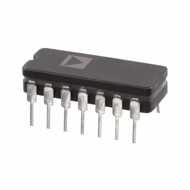
| 描述 | IC LOGIC PLL W/VCO 16SO锁相环 - PLL Hi-Spd CMOS Logic PLL w/VCO |
| 产品分类 | |
| 品牌 | Texas Instruments |
| 产品手册 | |
| 产品图片 |
|
| rohs | 符合RoHS无铅 / 符合限制有害物质指令(RoHS)规范要求 |
| 产品系列 | RF集成电路,锁相环 - PLL,Texas Instruments SN74LV4046ANSR74LV |
| 数据手册 | |
| 产品型号 | SN74LV4046ANSR |
| PLL | 是 |
| 产品目录页面 | |
| 产品种类 | 锁相环 - PLL |
| 供应商器件封装 | 16-SO |
| 其它名称 | 296-21050-1 |
| 分频器/倍频器 | 无/无 |
| 包装 | 剪切带 (CT) |
| 单位重量 | 200.700 mg |
| 商标 | Texas Instruments |
| 安装类型 | 表面贴装 |
| 安装风格 | SMD/SMT |
| 封装 | Reel |
| 封装/外壳 | 16-SOIC(0.209",5.30mm 宽) |
| 封装/箱体 | SOP-16 |
| 工作温度 | -40°C ~ 125°C |
| 工作电源电压 | 3.3 V, 5 V |
| 工厂包装数量 | 2000 |
| 差分-输入:输出 | 无/无 |
| 最大工作温度 | + 125 C |
| 最小工作温度 | - 40 C |
| 标准包装 | 1 |
| 比率-输入:输出 | 1:3 |
| 电压-电源 | 3 V ~ 5.5 V |
| 电源电压-最大 | 5.5 V |
| 电源电压-最小 | 3 V |
| 电路数 | 1 |
| 电路数量 | 1 |
| 类型 | 锁相环路(PLL) |
| 系列 | SN74LV4046A |
| 输入 | CMOS,TTL |
| 输出 | CMOS,TTL |
| 频率-最大值 | 38MHz |


PDF Datasheet 数据手册内容提取
Product Sample & Technical Tools & Support & Folder Buy Documents Software Community SN74LV4046A SCES656E–FEBRUARY2006–REVISEDNOVEMBER2016 SN74LV4046A High-Speed CMOS Logic Phase-Locked Loop With VCO 1 Features The signal input can be directly coupled to large voltage signals, or indirectly coupled (with a series • ESDProtectionExceedsJESD22 1 capacitor) to small voltage signals. A self-bias input – 2000-VHumanBodyModel(A114-A) circuit keeps small voltage signals within the linear – 1000-VCharged-DeviceModel(C101) region of the input amplifiers. With a passive low- pass filter, the SN74LV4046A forms a second-order • ChoiceofThreePhaseComparators loop PLL. The excellent VCO linearity is achieved by – ExclusiveOR the use of linear operational amplifier techniques. – Edge-TriggeredJ-KFlip-Flop Various applications include telecommunications, digitalphase-lockedloopandsignalgenerators. – Edge-TriggeredRSFlip-Flop • ExcellentVCOFrequencyLinearity DeviceInformation(1) • VCO-InhibitControlforON/OFFKeyingandfor PARTNUMBER PACKAGE BODYSIZE(NOM) LowStandbyPowerConsumption SN74LV4046ANS SO(16) 7.70mm×10.20mm • OptimizedPower-SupplyVoltageRangeFrom SN74LV4046AD SOIC(16) 6.00mm×9.90mm 3Vto5.5V SN74LV4046APW TSSOP(16) 6.40mm×5.00mm • WideOperatingTemperatureRangeFrom SN74LV4046ADGVR TVSOP(16) 3.60mm×4.40mm –40°Cto+125°C SN74LV4046AN PDIP(16) 19.30mm×6.35mm • Latch-UpPerformanceExceeds250mAPer (1) For all available packages, see the orderable addendum at JESD17 theendofthedatasheet. 2 Applications SN74LV4046AFunctionalBlockDiagram • Telecommunications V CC • SignalGenerators 16 • DigitalPhase-LockedLoop Phase 2 PC1 OUT Comparator 3 Description 1 The SN74LV4046A is a high-speed silicon-gate CMOS device that is pin compatible with the SIGIN 14 Phase 13 PC2OUT CD4046B and the CD74HC4046. The device is Comparator specifiedincompliancewithJEDECStd7. COMPIN 3 2 1 PCPOUT The SN74LV4046A is a phase-locked loop (PLL) Phase 15 PC3 OUT circuit that contains a linear voltage-controlled Comparator oscillator (VCO) and three different phase VCOIN 9 3 comparators (PC1, PC2, and PC3). A signal input INH 5 4 VCO and a comparator input are common to each OUT Voltage comparator. C1A 6 Controlled Oscillator 10 DEM C1 7 OUT B R 11 1 R 12 2 8 GND 1 An IMPORTANT NOTICE at the end of this data sheet addresses availability, warranty, changes, use in safety-critical applications, intellectualpropertymattersandotherimportantdisclaimers.PRODUCTIONDATA.
SN74LV4046A SCES656E–FEBRUARY2006–REVISEDNOVEMBER2016 www.ti.com Table of Contents 1 Features.................................................................. 1 7.4 DeviceFunctionalModes........................................11 2 Applications........................................................... 1 8 ApplicationandImplementation........................ 12 3 Description............................................................. 1 8.1 ApplicationInformation............................................12 4 RevisionHistory..................................................... 2 8.2 TypicalApplication .................................................12 5 PinConfigurationandFunctions......................... 3 9 PowerSupplyRecommendations...................... 14 6 Specifications......................................................... 4 10 Layout................................................................... 14 6.1 AbsoluteMaximumRatings.....................................4 10.1 LayoutGuidelines.................................................14 6.2 ESDRatings..............................................................4 10.2 LayoutExample....................................................14 6.3 RecommendedOperatingConditions.......................4 11 DeviceandDocumentationSupport................. 15 6.4 ThermalInformation..................................................4 11.1 DocumentationSupport........................................15 6.5 ElectricalCharacteristics...........................................5 11.2 ReceivingNotificationofDocumentationUpdates15 6.6 SwitchingCharacteristics..........................................6 11.3 CommunityResources..........................................15 6.7 TypicalCharacteristics..............................................9 11.4 Trademarks...........................................................15 7 DetailedDescription............................................ 10 11.5 ElectrostaticDischargeCaution............................15 7.1 Overview.................................................................10 11.6 Glossary................................................................15 7.2 FunctionalBlockDiagram.......................................10 12 Mechanical,Packaging,andOrderable Information........................................................... 15 7.3 FeatureDescription.................................................11 4 Revision History NOTE:Pagenumbersforpreviousrevisionsmaydifferfrompagenumbersinthecurrentversion. ChangesfromRevisionD(September2015)toRevisionE Page • Deleted200-VMachineModel(A115-A)fromFeatures........................................................................................................ 1 • AddedTVSOPandPDIPpackagestoDeviceInformationtable........................................................................................... 1 • AddedTVSOP,SO,andPDIPpackagestopinout................................................................................................................ 3 • ChangedR forDpackagefrom73°C/Wto82.8°C/W........................................................................................................ 4 θJA • ChangedR forDGVpackagefrom120°C/Wto116.8°C/W.............................................................................................. 4 θJA • ChangedR forNSpackagefrom64°C/Wto83.5°C/W..................................................................................................... 4 θJA • ChangedR forPWpackagefrom108°C/Wto108.1°C/W................................................................................................ 4 θJA • AddedvaluesintheThermalInformationtabletoalignwithJEDECstandards ................................................................... 4 • Changedx-axisfrom"–360°0°360°"to"0°90°180°" ......................................................................................................... 9 • Changed"(V /4)"to"(V /4π)".............................................................................................................................................. 9 CC CC • AddedReceivingNotificationofDocumentationUpdatessection....................................................................................... 15 ChangesfromRevisionC(April2007)toRevisionD Page • AddedPinConfigurationandFunctionssection,ESDRatingstable,FeatureDescriptionsection,DeviceFunctional Modes,ApplicationandImplementationsection,PowerSupplyRecommendationssection,Layoutsection,Device andDocumentationSupportsection,andMechanical,Packaging,andOrderableInformationsection .............................. 1 2 SubmitDocumentationFeedback Copyright©2006–2016,TexasInstrumentsIncorporated ProductFolderLinks:SN74LV4046A
SN74LV4046A www.ti.com SCES656E–FEBRUARY2006–REVISEDNOVEMBER2016 5 Pin Configuration and Functions D,DGV,NS,N,orPWPackage 16-PinSOIC,TVSOP,SO,PDIP,orTSSOP TopView PCPOUT 1 16 VCC PC1OUT 2 15 PC3OUT COMPIN 3 14 SIGIN VCOOUT 4 13 PC2OUT INH 5 12 R2 C1A 6 11 R1 C1 7 10 DEM B OUT GND 8 9 VCO IN PinFunctions PIN I/O DESCRIPTION NO. NAME 1 PCP O Phasecomparatorpulseoutput OUT 2 PC1 O Phasecomparator1output OUT 3 COMP I Comparatorinput IN 4 VCO O VCOoutput OUT 5 INH I Inhibitinput 6 C1 — CapacitorC1connectionA A 7 C1 — CapacitorC1connectionB B 8 GND — Ground(0V) 9 VCO I VCOinput IN 10 DEM O Demodulatoroutput OUT 11 R — ResistorR1connection 1 12 R — ResistorR2connection 2 13 PC2 O Phasecomparator2output OUT 14 SIG I Signalinput IN 15 PC3 O Phasecomparator3output OUT 16 V — Positivesupplyvoltage CC Copyright©2006–2016,TexasInstrumentsIncorporated SubmitDocumentationFeedback 3 ProductFolderLinks:SN74LV4046A
SN74LV4046A SCES656E–FEBRUARY2006–REVISEDNOVEMBER2016 www.ti.com 6 Specifications 6.1 Absolute Maximum Ratings overoperatingfree-airtemperaturerange(unlessotherwisenoted)(1) MIN MAX UNIT V DCsupplyvoltage –0.5 7 V CC V Inputvoltage –0.5 V +0.5 V I CC V Outputvoltage –0.5 V +0.5 V O CC I Inputclampcurrent V <0 –20 mA IK I I Outputclampcurrent V <0 –50 mA OK O I Continuousoutputcurent V =0toV ±35 mA O O CC I DCV orgroundcurrent ±70 mA CC CC T Junctiontemperature 150 °C J T Storagetemperature –65 150 °C stg (1) StressesbeyondthoselistedunderAbsoluteMaximumRatingsmaycausepermanentdamagetothedevice.Thesearestressratings only,andfunctionaloperationofthedeviceattheseoranyotherconditionsbeyondthoseindicatedunderRecommendedOperating Conditionsisnotimplied.Exposuretoabsolute-maximum-ratedconditionsforextendedperiodsmayaffectdevicereliability. 6.2 ESD Ratings VALUE UNIT Humanbodymodel(HBM),perANSI/ESDA/JEDECJS-001(1) ±2000 V Electrostaticdischarge V (ESD) Charged-devicemodel(CDM),perJEDECspecificationJESD22-C101(2) ±1000 (1) JEDECdocumentJEP155statesthat500-VHBMallowssafemanufacturingwithastandardESDcontrolprocess. (2) JEDECdocumentJEP157statesthat250-VCDMallowssafemanufacturingwithastandardESDcontrolprocess. 6.3 Recommended Operating Conditions overoperatingfree-airtemperaturerange(unlessotherwisenoted) MIN MAX UNIT T Operatingfree-airtemperature –40 125 °C A V Supplyvoltage 3 5.5 V CC V,V DCinputoroutputvoltage 0 V V I O CC 6.4 Thermal Information SN74LV4046A THERMALMETRIC(1) D(SOIC) DGV(TVSOP) NS(SO) PW(TSSOP) N(PDIP) UNIT 16PINS 16PINS 16PINS 16PINS 16PINS Junction-to-ambientthermal R 82.8 116.8 83.5 108.1 49.4 °C/W θJA resistance Junction-to-case(top)thermal R 44.0 43.3 41.7 42.7 36.7 °C/W θJC(top) resistance R Junction-to-boardthermalresistance 40.3 48.3 43.8 53.1 29.3 °C/W θJB Junction-to-topcharacterization ψ 11.1 3.7 9.3 4.2 21.5 °C/W JT parameter Junction-to-boardcharacterization ψ 40.0 47.8 43.5 52.5 29.2 °C/W JB parameter (1) Formoreinformationabouttraditionalandnewthermalmetrics,seetheSemiconductorandICPackageThermalMetricsapplication report. 4 SubmitDocumentationFeedback Copyright©2006–2016,TexasInstrumentsIncorporated ProductFolderLinks:SN74LV4046A
SN74LV4046A www.ti.com SCES656E–FEBRUARY2006–REVISEDNOVEMBER2016 6.5 Electrical Characteristics overoperatingfree-airtemperaturerange(unlessotherwisenoted) TESTCONDITIONS PARAMETER VCC(V) MIN TYP MAX UNIT VI(V) IO(mA) VCO 3to3.6 VCC×0.7 VIH High-levelinputvoltage INH V 4.5to5.5 VCC×0.7 3to5.5 VCC×0.3 VIL Low-levelinputvoltage INH V 4.5to5.5 VCC×0.3 3to3.6 VCC–0.1 High-level CMOS –0.05 VOH outputvoltage VCOOUT VILorVIH 4.5to5.5 VCC–0.1 V TTL –12 4.5to5.5 3.8 3to3.6 0.1 CMOS 0.05 VCOOUT 4.5to5.5 0.1 Low-level VOL outputvoltage TTL VILorVIH 12 4.5to5.5 0.55 V C1A,C1B 12 4.5to5.5 0.65 (testpurposesonly) II Inputleakagecurrent INH,VCOIN VCCorGND 5.5 ±1 μA R1range(1) 3to5.5 3 50 kΩ R2range(1) 3to5.5 3 50 kΩ 3to3.6 40 NoLimit C1capacitancerange pF 4.5to5.5 40 NoLimit Overtherangespecifiedfor 3to3.6 1.1 1.9 Operatingvoltagerange VCOIN R1forlinearity(2) 4.5to5.5 1.1 3.2 V PHASECOMPARATOR VIH DinCpu-ctovuopltlaegdehigh-level SCIOGMINP,IN 43.5toto35.6.5 VVCCCC××00..77 VIL DC-coupledlow-levelinputvoltage SCIOGMINP,IN 43.5toto35.6.5 VVCCCC××00..33 V –0.05 3to5.5 VCC–0.1 VOH Houigtphu-ltevvoelltage PPCCPNOOUUTT, CMOS VILorVIH –6 3to3.6 2.48 V TTL –12 4.5to5.5 3.8 3to3.6 0.1 VOL Loouwtp-uletvveolltage PPCCPNOOUUTT, CMOS VILorVIH 0.02 4.5to5.5 0.1 V TTL 4 4.5to5.5 0.4 II Inputleakagecurrent SCIOGMINP,IN VCCorGND 43.5toto35.6.5 ±±1219 μA IOZ 3-stateoff-statecurrent PC2OUT VILorVIH 3to5.5 ±5 μA RI Inputresistance SCIOGMINP,IN VIaptoseinlft-,bViaIs=o0p.5erVating 43.5 820500 kΩ DEMODULATOR RS>300kΩ,Leakage 3to3.6 50 300 RS Resistorrange currentcaninfluence kΩ VDEMOUT 4.5to5.5 50 300 VOFF OffsetvoltageVCOINtoVDEM VI=taVkVeCnOIoNv=erVRCSC/r2a,nVgaelues 43.5toto35.6.5 ±±3200 mV Pins3,5,and14atVCC, ICC Quiescentdevicecurrent Pin9atGND,IIatpins3 5.5 50 μA and14tobeexcluded (1) ThevalueforR1andR2inparallelshouldexceed2.7kΩ. (2) ThemaximumoperatingvoltagecanbeashighasV –0.9V;however,thismayresultinanincreasedoffsetvoltage. CC Copyright©2006–2016,TexasInstrumentsIncorporated SubmitDocumentationFeedback 5 ProductFolderLinks:SN74LV4046A
SN74LV4046A SCES656E–FEBRUARY2006–REVISEDNOVEMBER2016 www.ti.com 6.6 Switching Characteristics overoperatingfree-airtemperaturerange(unlessotherwisenoted)C =50pF,Inputt,t =6ns L r f V PARAMETER TESTCONDITIONS CC MIN TYP MAX UNIT (V) PHASECOMPARATOR SIG ,COMP to 3to3.6 135 t ,t Propagationdelay IN IN ns PLH PHL PC1OUT 4.5to5.5 50 SIGIN,COMP to 3to3.6 300 t ,t Propagationdelay IN ns PLH PHL PCPOUT 4.5to5.5 60 SIG ,COMP to 3to3.6 200 t ,t Propagationdelay IN IN ns PLH PHL PC3OUT 4.5to5.5 50 3to3.6 75 t ,t Outputtransitiontime ns THL TLH 4.5to5.5 15 SIG ,COMP to 3to3.6 270 t ,t 3-stateoutputenabletime IN IN ns PZH PZL PC2OUT 4.5to5.5 54 SIG ,COMP to 3to3.6 320 t ,t 3-stateoutputdisabletime IN IN ns PHZ PLZ PC2OUT 4.5to5.5 65 (P-P)atSIG or 3to3.6 11 AC-coupledinputsensitivity IN V mV COMPIN I(P-P) 4.5to5.5 15 VCO V =VCO =1/2V , 3to3.6 0.11 I IN CC R =100kΩ, Δf/ΔT Frequencystabilitywithtemperaturechange 1 %/°C R2=∞, 4.5to5.5 0.11 C =100pF 1 C =50pF, 3to3.6 24 1 R =3.5kΩ, 1 R =∞ 4.5to5.5 24 2 f Maximumfrequency MHz MAX C =0pF, 3to3.6 38 1 R =9.1kΩ, 1 R2=∞ 4.5to5.5 38 C =40pF, 3to3.6 7 10 1 R =3kΩ, Centerfrequency(duty50%) 1 4.5to5.5 12 17 MHz R =∞, 2 VCO =V /2 4.5(1) 15(1) 17.5(1) IN CC C =100pF, 3to3.6 0.4% 1 ΔfVCO Frequencylinearity R =100kΩ, 1 R =∞ 4.5to5.5 0.4% 2 C =1nF, 3to3.6 400 Offsetfrequency 1 kHz R2=220kΩ 4.5to5.5 400 DEMODULATOR C =100pF, 3 8 1 C =100pF, 2 V vsf R =100kΩ, mV/kHz OUT IN 1 R =∞, 4.5 330 2 R =100kΩ 3 (1) Dataisspecifiedat25°C 6 SubmitDocumentationFeedback Copyright©2006–2016,TexasInstrumentsIncorporated ProductFolderLinks:SN74LV4046A
SN74LV4046A www.ti.com SCES656E–FEBRUARY2006–REVISEDNOVEMBER2016 SIG IN COMP IN VCO OUT PC1 OUT VCC VCO IN GND LoopLockedatf o Figure1. TypicalWaveformsforPLLUsing PhaseComparator1 SIGIN COMPIN VCOOUT VCC PC2OUT GND High-Impedance Off State VCOIN PCPOUT LoopLockedatf o Figure2. TypicalWaveformsforPLLUsing PhaseComparator2 SIG IN COMP IN VCO OUT PC3 OUT V VCO CC IN GND LoopLockedatf o Figure3. TypicalWaveformsforPLLUsing PhaseComparator3 Copyright©2006–2016,TexasInstrumentsIncorporated SubmitDocumentationFeedback 7 ProductFolderLinks:SN74LV4046A
SN74LV4046A SCES656E–FEBRUARY2006–REVISEDNOVEMBER2016 www.ti.com SIGIN, COMPIN VS Inputs tPHL tPLH PCPOUT, PC1OUT, PC3OUT VS Outputs tTHL tTLH Figure4. Input-to-OutputPropagationDelaysand OutputTransitionTimes SIGIN Inputs VS COMPIN Inputs VS tPHZ tPLZ tPZH tPZL PC2OUT 90% Output VS 10% Figure5. 3-StateEnableandDisableTimesforPC2 OUT 8 SubmitDocumentationFeedback Copyright©2006–2016,TexasInstrumentsIncorporated ProductFolderLinks:SN74LV4046A
SN74LV4046A www.ti.com SCES656E–FEBRUARY2006–REVISEDNOVEMBER2016 6.7 Typical Characteristics VCC VCC VDEMOUT (AV) VDEMOUT (AV) 1/2 VCC 1/2 VCC 0 0 0° 90° φDEMOUT 180° -360° 0° φDEMOUT 360° PhaseComparator1: PhaseComparator2: V =V =(V /π)(SIG –COMP ); V =V =(V /4π)(SIG –COMP ); DEMOUT PC1OUT CC IN IN DEMOUT PC2OUT CC IN IN DEMOUT=(SIG –COMP ) DEMOUT=(SIG –COMP ) IN IN IN IN Figure6.AverageOutputVoltagevsInputPhaseDifference Figure7.AverageOutputVoltagevsInputPhaseDifference VCC VDEMOUT(AV) 1/2 VCC 0 0° 180° φDEMOUT 360° PhaseComparator3: V =V =(V /2π)(SIG –COMP ); DEMOUT PC3OUT CC IN IN DEMOUT=(SIG –COMP ) IN IN Figure8.AverageOutputVoltagevsInputPhaseDifference Copyright©2006–2016,TexasInstrumentsIncorporated SubmitDocumentationFeedback 9 ProductFolderLinks:SN74LV4046A
SN74LV4046A SCES656E–FEBRUARY2006–REVISEDNOVEMBER2016 www.ti.com 7 Detailed Description 7.1 Overview The SN74LV4046A is a high-speed silicon-gate CMOS device that is pin compatible with the CD4046B and the CD74HC4046.ThedeviceisspecifiedincompliancewithJEDECStd7. The SN74LV4046A is a phase-locked loop (PLL) circuit that contains a linear voltage-controlled oscillator (VCO) and three different phase comparators (PC1, PC2, and PC3) as explained in the Features section. A signal input andacomparatorinputarecommontoeachcomparatorasshownintheFunctionalBlockDiagram. The signal input can be directly coupled to large voltage signals, or indirectly coupled (with a series capacitor) to small voltage signals. A self-bias input circuit keeps small voltage signals within the linear region of the input amplifiers. With a passive lowpass filter, the SN74LV4046A forms a second-order loop PLL. The excellent VCO linearity is achieved by the use of linear operational amplifier techniques. Various applications include telecommunications,DigitalPhaseLockedLoopandSignalgenerators. The VCO requires one external capacitor C1 (between C1A and C1B) and one external resistor R1 (between R1 and GND) or two external resistors R1 and R2 (between R1 and GND, and R2 and GND). Resistor R1 and capacitor C1 determine the frequency range of the VCO. Resistor R2 enables the VCO to have a frequency offset if required. The high input impedance of the VCO simplifies the design of lowpass filters by giving the designer a wide choice of resistor or capacitor ranges. In order to not load the lowpass filter, a demodulator outputoftheVCOinputvoltageisprovidedatpin10(DEM ).Incontrasttoconventionaltechniqueswherethe OUT DEM voltageisonethresholdvoltagelowerthantheVCOinputvoltage,heretheDEM voltageequalsthat OUT OUT of the VCO input. If DEM is used, a load resistor (R ) should be connected from DEM to GND; if unused, OUT S OUT DEM should be left open. The VCO output (VCO ) can be connected directly to the comparator input OUT OUT (COMP ), or connected through a frequency divider. The VCO output signal has a specified duty factor of 50%. IN A LOW level at the inhibit input (INH) enables the VCO and demodulator, while a HIGH level turns both off to minimizestandbypowerconsumption. 7.2 Functional Block Diagram V CC 16 Phase 2 PC1 OUT Comparator 1 SIG 14 Phase 13 PC2 IN OUT Comparator COMPIN 3 2 1 PCPOUT Phase 15 PC3 OUT Comparator VCOIN 9 3 INH 5 4 VCO OUT Voltage C1 6 A Controlled Oscillator 10 DEM C1 7 OUT B R 11 1 R 12 2 8 GND 10 SubmitDocumentationFeedback Copyright©2006–2016,TexasInstrumentsIncorporated ProductFolderLinks:SN74LV4046A
SN74LV4046A www.ti.com SCES656E–FEBRUARY2006–REVISEDNOVEMBER2016 7.3 Feature Description TherearethreechoicesforthePhaseComparatorsinthisdevicewhicharelistedasfollows: • Phase comparator 1 (PC1) is an Exclusive OR network. The average output voltage from PC1, fed to VCO input through the low pass filter and seen at the demodulator output at pin 10 (V ), is the resultant of DEMOUT the phase differences of signals (SIG ) and the compartor input (COMP ) as shown in Figure 7. The IN IN average of V is equal to 1/2 VCC when there is no signal or noise at SIG , and with this input the VCO DEM IN oscillatesatthecenterfrequency(fo). • Phase comparator 2 (PC2) is an Edge-Triggered Flip-Flop. This is a positive edge-triggered phase and frequencydetector.WhenthePLLisusingthiscomparator,theloopiscontrolledbypositivesignaltransitions and the duty factors of SIG and COMP are not important. PC2 comprises two D-type flip-flops, control- IN IN gatingandathree-stateoutputstage.Thecircuitfunctionsasanup-downcounterwhereSIG causesanup- IN count and COMP a down-count. The average output voltage from PC2, fed to the VCO through the lowpass IN filter and seen at the demodulator output at pin 10 (V ), is the resultant of the phase differences of DEMOUT SIG andCOMP asinFigure8. IN IN • Phase comparator 3 (PC3) is an positive Edge-Triggered RS Flip-Flop. This is a positive edge-triggered sequential phase detector using an RS-type flip-flop. When the PLL is using this comparator, the loop is controlled by positive signal transitions and the duty factors of SIG and COMP are not important. The IN IN average output from PC3, fed to the VCO through the lowpass filter and seen at the demodulator at pin 10 (V ),istheresultantofthephasedifferencesofSIG andCOMP asshowninFigure9. DEMOUT IN IN The excellent VCO linearity is achieved by the use of linear operational amplifier techniques. It has low standby power consumption using VCO inhibit control. Wide operating temperature range from –40°C to +125°C along withanoptimizedpowersupplyvoltagerangefrom3Vto5.5V. 7.4 Device Functional Modes TheSN74LV4046Adevicedoesnotfeatureanyspecialfunctionalmodes. Copyright©2006–2016,TexasInstrumentsIncorporated SubmitDocumentationFeedback 11 ProductFolderLinks:SN74LV4046A
SN74LV4046A SCES656E–FEBRUARY2006–REVISEDNOVEMBER2016 www.ti.com 8 Application and Implementation NOTE Information in the following applications sections is not part of the TI component specification, and TI does not warrant its accuracy or completeness. TI’s customers are responsible for determining suitability of components for their purposes. Customers should validateandtesttheirdesignimplementationtoconfirmsystemfunctionality. 8.1 Application Information The most common use for the digital phased-locked loop (PLL) device is to match the VCO output to the same phase as the incoming signal and produce an error signal (DEM ) that indicates the amount of phase shift OUT requiredforthematch.Thiscanbeusedaspartofmanycomplexsystems. 8.2 Typical Application VCC 16 Phase 2 PC1OUT Comparator 1 Input COSMIGPIINN 134 CoPmhp2aasreator 113 PPCC2POOUUTT RC32 Phase 15 PC3OUT VCOOUT Comparator 4 3 INH 5 9 VCOIN C1A Voltage C1 C1B 76 COosnctirlloaltleodr 10 DEMOUT R1 11 R5 R2 12 R1 R2 8 GND Figure9. SN74LV4046ADigitalClockSignalPhaseComparisonApplication 12 SubmitDocumentationFeedback Copyright©2006–2016,TexasInstrumentsIncorporated ProductFolderLinks:SN74LV4046A
SN74LV4046A www.ti.com SCES656E–FEBRUARY2006–REVISEDNOVEMBER2016 Typical Application (continued) 8.2.1 DesignRequirements Table1andTable2liststhedesignrequirementsoftheSN74LV4046A. Table1.ComponentSelectionCriteria(1) COMPONENT VALUE R1 3kΩto50kΩ R2 3kΩto50kΩ R1||R2 >2.7kΩ C1 >40pF R3 1kΩ C2 1uF R5 50kΩto300kΩ (1) R1between3kΩand50kΩ R2between3kΩand50kΩ R1+R2parallelvalue>2.7kΩ C1>40pF Table2.C (1) PD CHIPSECTION C UNIT PD Comparator1 120 pF VCO 120 (1) R1between3kΩand50kΩ R2between3kΩand50kΩ R1+R2parallelvalue>2.7kΩ C1>40pF 8.2.2 DetailedDesignProcedure 1. RecommendedInputConditions: – V andV foreachinputcanbefoundinElectricalCharacteristics. IH IL 2. RecommendedOutputConditions: – ValidloadresistorvaluesarespecifiedinElectricalCharacteristics. 3. FrequencySelectionCriterion: – FrequencydataisfoundinElectricalCharacteristics. 8.2.3 ApplicationCurves Table3liststheapplicationcurvesintheTypicalCharacteristics section. Table3.TableofGraphs GRAPHTITLE FIGURE AverageOutputVoltagevsInputPhaseDifference Figure6 AverageOutputVoltagevsInputPhaseDifference Figure7 AverageOutputVoltagevsInputPhaseDifference Figure8 Copyright©2006–2016,TexasInstrumentsIncorporated SubmitDocumentationFeedback 13 ProductFolderLinks:SN74LV4046A
SN74LV4046A SCES656E–FEBRUARY2006–REVISEDNOVEMBER2016 www.ti.com 9 Power Supply Recommendations The power supply can be any voltage between the minimum and maximum supply voltage ratings located in the RecommendedOperatingConditionstable. Each V pin should have a good bypass capacitor to prevent power disturbance. For devices with a single CC supply. a 0.1-µF capacitor is recommended and if there are multiple V pins then 0.01-µF or 0.022-µF capacitor CC is recommended for each power pin. It is ok to parallel multiple bypass capacitors to reject different frequencies of noise. 0.1-µF and 1-µF capacitors are commonly used in parallel. The bypass capacitor should be installed as closetothepowerpinaspossibleforbestresults. 10 Layout 10.1 Layout Guidelines Reflections and matching are closely related to the loop antenna theory but are different enough to be discussed separately from the theory. When a PCB trace turns a corner at a 90° angle, a reflection can occur. A reflection occurs primarily because of the change of width of the trace. At the apex of the turn, the trace width increases to 1.414 times the width. This increase upsets the transmission-line characteristics, especially the distributed capacitance and self–inductance of the trace which results in the reflection. Not all PCB traces can be straight and therefore some traces must turn corners. Figure 10 shows progressively better techniques of rounding corners.Onlythelastexample(BEST)maintainsconstanttracewidthandminimizesreflections. 10.2 Layout Example WORST BETTER BEST W 2 1W min. W Figure10. TraceExample 14 SubmitDocumentationFeedback Copyright©2006–2016,TexasInstrumentsIncorporated ProductFolderLinks:SN74LV4046A
SN74LV4046A www.ti.com SCES656E–FEBRUARY2006–REVISEDNOVEMBER2016 11 Device and Documentation Support 11.1 Documentation Support 11.1.1 RelatedDocumentation Forrelateddocumentationseethefollowing: ImplicationsofSloworFloatingCMOSInputs,SCBA004 11.2 Receiving Notification of Documentation Updates To receive notification of documentation updates, navigate to the device product folder on ti.com. In the upper right corner, click on Alert me to register and receive a weekly digest of any product information that has changed.Forchangedetails,reviewtherevisionhistoryincludedinanyreviseddocument. 11.3 Community Resources The following links connect to TI community resources. Linked contents are provided "AS IS" by the respective contributors. They do not constitute TI specifications and do not necessarily reflect TI's views; see TI's Terms of Use. TIE2E™OnlineCommunity TI'sEngineer-to-Engineer(E2E)Community.Createdtofostercollaboration amongengineers.Ate2e.ti.com,youcanaskquestions,shareknowledge,exploreideasandhelp solveproblemswithfellowengineers. DesignSupport TI'sDesignSupport QuicklyfindhelpfulE2Eforumsalongwithdesignsupporttoolsand contactinformationfortechnicalsupport. 11.4 Trademarks E2EisatrademarkofTexasInstruments. Allothertrademarksarethepropertyoftheirrespectiveowners. 11.5 Electrostatic Discharge Caution Thesedeviceshavelimitedbuilt-inESDprotection.Theleadsshouldbeshortedtogetherorthedeviceplacedinconductivefoam duringstorageorhandlingtopreventelectrostaticdamagetotheMOSgates. 11.6 Glossary SLYZ022—TIGlossary. Thisglossarylistsandexplainsterms,acronyms,anddefinitions. 12 Mechanical, Packaging, and Orderable Information The following pages include mechanical, packaging, and orderable information. This information is the most current data available for the designated devices. This data is subject to change without notice and revision of thisdocument.Forbrowser-basedversionsofthisdatasheet,refertotheleft-handnavigation. Copyright©2006–2016,TexasInstrumentsIncorporated SubmitDocumentationFeedback 15 ProductFolderLinks:SN74LV4046A
PACKAGE OPTION ADDENDUM www.ti.com 6-Feb-2020 PACKAGING INFORMATION Orderable Device Status Package Type Package Pins Package Eco Plan Lead/Ball Finish MSL Peak Temp Op Temp (°C) Device Marking Samples (1) Drawing Qty (2) (6) (3) (4/5) SN74LV4046AD ACTIVE SOIC D 16 40 Green (RoHS NIPDAU Level-1-260C-UNLIM -40 to 85 LV4046A & no Sb/Br) SN74LV4046ADGVR ACTIVE TVSOP DGV 16 2000 Green (RoHS NIPDAU Level-1-260C-UNLIM -40 to 85 LW046A & no Sb/Br) SN74LV4046ADR ACTIVE SOIC D 16 2500 Green (RoHS NIPDAU Level-1-260C-UNLIM -40 to 85 LV4046A & no Sb/Br) SN74LV4046ADRG4 ACTIVE SOIC D 16 2500 Green (RoHS NIPDAU Level-1-260C-UNLIM -40 to 85 LV4046A & no Sb/Br) SN74LV4046AN ACTIVE PDIP N 16 25 Green (RoHS NIPDAU N / A for Pkg Type -40 to 85 SN74LV4046AN & no Sb/Br) SN74LV4046ANE4 ACTIVE PDIP N 16 25 Green (RoHS NIPDAU N / A for Pkg Type -40 to 85 SN74LV4046AN & no Sb/Br) SN74LV4046ANS ACTIVE SO NS 16 50 Green (RoHS NIPDAU Level-1-260C-UNLIM -40 to 85 74LV4046A & no Sb/Br) SN74LV4046ANSR ACTIVE SO NS 16 2000 Green (RoHS NIPDAU Level-1-260C-UNLIM -40 to 85 74LV4046A & no Sb/Br) SN74LV4046APW ACTIVE TSSOP PW 16 90 Green (RoHS NIPDAU Level-1-260C-UNLIM -40 to 85 LW046A & no Sb/Br) SN74LV4046APWG4 ACTIVE TSSOP PW 16 90 Green (RoHS NIPDAU Level-1-260C-UNLIM -40 to 85 LW046A & no Sb/Br) SN74LV4046APWR ACTIVE TSSOP PW 16 2000 Green (RoHS NIPDAU Level-1-260C-UNLIM -40 to 85 LW046A & no Sb/Br) (1) The marketing status values are defined as follows: ACTIVE: Product device recommended for new designs. LIFEBUY: TI has announced that the device will be discontinued, and a lifetime-buy period is in effect. NRND: Not recommended for new designs. Device is in production to support existing customers, but TI does not recommend using this part in a new design. PREVIEW: Device has been announced but is not in production. Samples may or may not be available. OBSOLETE: TI has discontinued the production of the device. (2) RoHS: TI defines "RoHS" to mean semiconductor products that are compliant with the current EU RoHS requirements for all 10 RoHS substances, including the requirement that RoHS substance do not exceed 0.1% by weight in homogeneous materials. Where designed to be soldered at high temperatures, "RoHS" products are suitable for use in specified lead-free processes. TI may reference these types of products as "Pb-Free". RoHS Exempt: TI defines "RoHS Exempt" to mean products that contain lead but are compliant with EU RoHS pursuant to a specific EU RoHS exemption. Green: TI defines "Green" to mean the content of Chlorine (Cl) and Bromine (Br) based flame retardants meet JS709B low halogen requirements of <=1000ppm threshold. Antimony trioxide based flame retardants must also meet the <=1000ppm threshold requirement. Addendum-Page 1
PACKAGE OPTION ADDENDUM www.ti.com 6-Feb-2020 (3) MSL, Peak Temp. - The Moisture Sensitivity Level rating according to the JEDEC industry standard classifications, and peak solder temperature. (4) There may be additional marking, which relates to the logo, the lot trace code information, or the environmental category on the device. (5) Multiple Device Markings will be inside parentheses. Only one Device Marking contained in parentheses and separated by a "~" will appear on a device. If a line is indented then it is a continuation of the previous line and the two combined represent the entire Device Marking for that device. (6) Lead/Ball Finish - Orderable Devices may have multiple material finish options. Finish options are separated by a vertical ruled line. Lead/Ball Finish values may wrap to two lines if the finish value exceeds the maximum column width. Important Information and Disclaimer:The information provided on this page represents TI's knowledge and belief as of the date that it is provided. TI bases its knowledge and belief on information provided by third parties, and makes no representation or warranty as to the accuracy of such information. Efforts are underway to better integrate information from third parties. TI has taken and continues to take reasonable steps to provide representative and accurate information but may not have conducted destructive testing or chemical analysis on incoming materials and chemicals. TI and TI suppliers consider certain information to be proprietary, and thus CAS numbers and other limited information may not be available for release. In no event shall TI's liability arising out of such information exceed the total purchase price of the TI part(s) at issue in this document sold by TI to Customer on an annual basis. Addendum-Page 2
PACKAGE MATERIALS INFORMATION www.ti.com 26-Oct-2016 TAPE AND REEL INFORMATION *Alldimensionsarenominal Device Package Package Pins SPQ Reel Reel A0 B0 K0 P1 W Pin1 Type Drawing Diameter Width (mm) (mm) (mm) (mm) (mm) Quadrant (mm) W1(mm) SN74LV4046ADGVR TVSOP DGV 16 2000 330.0 12.4 6.8 4.0 1.6 8.0 12.0 Q1 SN74LV4046ADR SOIC D 16 2500 330.0 16.4 6.5 10.3 2.1 8.0 16.0 Q1 SN74LV4046ANSR SO NS 16 2000 330.0 16.4 8.2 10.5 2.5 12.0 16.0 Q1 SN74LV4046APWR TSSOP PW 16 2000 330.0 12.4 6.9 5.6 1.6 8.0 12.0 Q1 PackMaterials-Page1
PACKAGE MATERIALS INFORMATION www.ti.com 26-Oct-2016 *Alldimensionsarenominal Device PackageType PackageDrawing Pins SPQ Length(mm) Width(mm) Height(mm) SN74LV4046ADGVR TVSOP DGV 16 2000 367.0 367.0 35.0 SN74LV4046ADR SOIC D 16 2500 333.2 345.9 28.6 SN74LV4046ANSR SO NS 16 2000 367.0 367.0 38.0 SN74LV4046APWR TSSOP PW 16 2000 367.0 367.0 35.0 PackMaterials-Page2
None
None
PACKAGE OUTLINE PW0016A TSSOP - 1.2 mm max height SCALE 2.500 SMALL OUTLINE PACKAGE SEATING PLANE C 6.6 TYP 6.2 A 0.1 C PIN 1 INDEX AREA 14X 0.65 16 1 2X 5.1 4.55 4.9 NOTE 3 8 9 0.30 B 4.5 16X 0.19 1.2 MAX 4.3 0.1 C A B NOTE 4 (0.15) TYP SEE DETAIL A 0.25 GAGE PLANE 0.15 0.05 0.75 0.50 0 -8 DETA 20AIL A TYPICAL 4220204/A 02/2017 NOTES: 1. All linear dimensions are in millimeters. Any dimensions in parenthesis are for reference only. Dimensioning and tolerancing per ASME Y14.5M. 2. This drawing is subject to change without notice. 3. This dimension does not include mold flash, protrusions, or gate burrs. Mold flash, protrusions, or gate burrs shall not exceed 0.15 mm per side. 4. This dimension does not include interlead flash. Interlead flash shall not exceed 0.25 mm per side. 5. Reference JEDEC registration MO-153. www.ti.com
EXAMPLE BOARD LAYOUT PW0016A TSSOP - 1.2 mm max height SMALL OUTLINE PACKAGE 16X (1.5) SYMM (R0.05) TYP 1 16X (0.45) 16 SYMM 14X (0.65) 8 9 (5.8) LAND PATTERN EXAMPLE EXPOSED METAL SHOWN SCALE: 10X SOLDER MASK METAL UNDER SOLDER MASK OPENING METAL SOLDER MASK OPENING EXPOSED METAL EXPOSED METAL 0.05 MAX 0.05 MIN ALL AROUND ALL AROUND NON-SOLDER MASK SOLDER MASK DEFINED DEFINED (PREFERRED) SOLDE15.000R MASK DETAILS 4220204/A 02/2017 NOTES: (continued) 6. Publication IPC-7351 may have alternate designs. 7. Solder mask tolerances between and around signal pads can vary based on board fabrication site. www.ti.com
EXAMPLE STENCIL DESIGN PW0016A TSSOP - 1.2 mm max height SMALL OUTLINE PACKAGE 16X (1.5) SYMM (R0.05) TYP 1 16X (0.45) 16 SYMM 14X (0.65) 8 9 (5.8) SOLDER PASTE EXAMPLE BASED ON 0.125 mm THICK STENCIL SCALE: 10X 4220204/A 02/2017 NOTES: (continued) 8. Laser cutting apertures with trapezoidal walls and rounded corners may offer better paste release. IPC-7525 may have alternate design recommendations. 9. Board assembly site may have different recommendations for stencil design. www.ti.com
None
None
IMPORTANTNOTICEANDDISCLAIMER TI PROVIDES TECHNICAL AND RELIABILITY DATA (INCLUDING DATASHEETS), DESIGN RESOURCES (INCLUDING REFERENCE DESIGNS), APPLICATION OR OTHER DESIGN ADVICE, WEB TOOLS, SAFETY INFORMATION, AND OTHER RESOURCES “AS IS” AND WITH ALL FAULTS, AND DISCLAIMS ALL WARRANTIES, EXPRESS AND IMPLIED, INCLUDING WITHOUT LIMITATION ANY IMPLIED WARRANTIES OF MERCHANTABILITY, FITNESS FOR A PARTICULAR PURPOSE OR NON-INFRINGEMENT OF THIRD PARTY INTELLECTUAL PROPERTY RIGHTS. These resources are intended for skilled developers designing with TI products. You are solely responsible for (1) selecting the appropriate TI products for your application, (2) designing, validating and testing your application, and (3) ensuring your application meets applicable standards, and any other safety, security, or other requirements. These resources are subject to change without notice. TI grants you permission to use these resources only for development of an application that uses the TI products described in the resource. Other reproduction and display of these resources is prohibited. No license is granted to any other TI intellectual property right or to any third party intellectual property right. TI disclaims responsibility for, and you will fully indemnify TI and its representatives against, any claims, damages, costs, losses, and liabilities arising out of your use of these resources. TI’s products are provided subject to TI’s Terms of Sale (www.ti.com/legal/termsofsale.html) or other applicable terms available either on ti.com or provided in conjunction with such TI products. TI’s provision of these resources does not expand or otherwise alter TI’s applicable warranties or warranty disclaimers for TI products. Mailing Address: Texas Instruments, Post Office Box 655303, Dallas, Texas 75265 Copyright © 2020, Texas Instruments Incorporated