ICGOO在线商城 > 集成电路(IC) > 逻辑 - 信号开关,多路复用器,解码器 > SN74LV138ADGVR

 Datasheet下载
- 型号: SN74LV138ADGVR
- 制造商: Texas Instruments
- 库位|库存: xxxx|xxxx
- 要求:
| 数量阶梯 | 香港交货 | 国内含税 |
| +xxxx | $xxxx | ¥xxxx |
查看当月历史价格
查看今年历史价格
SN74LV138ADGVR产品简介:
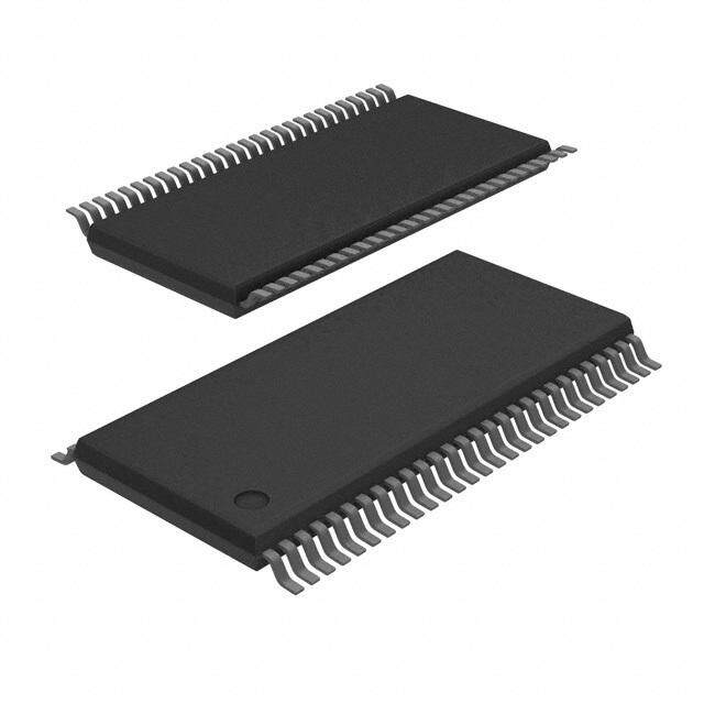
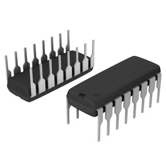
ICGOO电子元器件商城为您提供SN74LV138ADGVR由Texas Instruments设计生产,在icgoo商城现货销售,并且可以通过原厂、代理商等渠道进行代购。 SN74LV138ADGVR价格参考。Texas InstrumentsSN74LV138ADGVR封装/规格:逻辑 - 信号开关,多路复用器,解码器, Decoder/Demultiplexer 1 x 3:8 16-TVSOP。您可以下载SN74LV138ADGVR参考资料、Datasheet数据手册功能说明书,资料中有SN74LV138ADGVR 详细功能的应用电路图电压和使用方法及教程。
| 参数 | 数值 |
| 产品目录 | 集成电路 (IC)半导体 |
| 描述 | IC 3-TO-8 DECODER/DEMUX 16-TVSOP编码器、解码器、复用器和解复用器 3 to 8-Line Decdr/Demltplxer |
| 产品分类 | |
| 品牌 | Texas Instruments |
| 产品手册 | |
| 产品图片 |
|
| rohs | 符合RoHS无铅 / 符合限制有害物质指令(RoHS)规范要求 |
| 产品系列 | 逻辑集成电路,编码器、解码器、复用器和解复用器,Texas Instruments SN74LV138ADGVR74LV |
| 数据手册 | |
| 产品型号 | SN74LV138ADGVR |
| 产品 | Decoders / Demultiplexers |
| 产品目录页面 | |
| 产品种类 | 编码器、解码器、复用器和解复用器 |
| 供应商器件封装 | 16-TVSOP |
| 其它名称 | 296-23261-1 |
| 包装 | 剪切带 (CT) |
| 单位重量 | 42 mg |
| 商标 | Texas Instruments |
| 安装类型 | 表面贴装 |
| 安装风格 | SMD/SMT |
| 封装 | Reel |
| 封装/外壳 | 16-TFSOP (0.173",4.40mm 宽) |
| 封装/箱体 | TVSOP-16 |
| 工作温度 | -40°C ~ 85°C |
| 工作温度范围 | - 40 C to + 85 C |
| 工作电压 | 2 V to 5.5 V |
| 工厂包装数量 | 2000 |
| 最大工作温度 | + 85 C |
| 最小工作温度 | - 40 C |
| 标准包装 | 1 |
| 独立电路 | 1 |
| 电压-电源 | 2 V ~ 5.5 V |
| 电压源 | 单电源 |
| 电流-输出高,低 | 12mA,12mA |
| 电源电压-最大 | 5.5 V |
| 电源电压-最小 | 2 V |
| 电路 | 1 x 3:8 |
| 类型 | 解码器/多路分解器 |
| 系列 | SN74LV138A |
| 输入/输出线数量 | 3 / 8 |
| 输入线路数量 | 3 |
| 输出线路数量 | 8 |
| 逻辑系列 | LV-A |


PDF Datasheet 数据手册内容提取
SN54LV138A, SN74LV138A 3-LINE TO 8-LINE DECODERS/DEMULTIPLEXERS www.ti.com SCLS395L–APRIL1998–REVISEDAUGUST2005 FEATURES • 2-Vto5.5-VV Operation • I SupportsPartial-Power-DownMode CC off • Maxt of9.5nsat5V Operation pd • TypicalV (OutputGroundBounce) • Latch-UpPerformanceExceeds250mAPer OLP <0.8VatV =3.3V,T =25(cid:176) C JESD17 CC A • TypicalV (OutputV Undershoot) • ESDProtectionExceedsJESD22 OHV OH >2.3VatV =3.3V,T =25(cid:176) C – 2000-VHuman-BodyModel(A114-A) CC A • SupportMixed-ModeVoltageOperationonAll – 200-VMachineModel(A115-A) Ports – 1000-VCharged-DeviceModel(C101) SN54LV138A...J OR W PACKAGE SN74LV138A...RGY PACKAGE SN54LV138A...FK PACKAGE SN74LV138A...D, DB, DGV, NS (TOP VIEW) (TOP VIEW) OR PW PACKAGE (TOP VIEW) CC C CC0 A V B A N V Y A 1 16 VCC 1 16 3 2 1 20 19 B 2 15 Y0 B 2 15 Y0 C 4 18 Y1 C 3 14 Y1 C 3 14 Y1 G2A 5 17 Y2 G2A 4 13 Y2 G2A 4 13 Y2 NC 6 16 NC G2B 5 12 Y3 G2B 5 12 Y3 G2B 7 15 Y3 G1 6 11 Y4 G1 6 11 Y4 G1 8 14 Y4 9 10 1112 13 Y7 7 10 Y5 Y7 7 10 Y5 8 9 7D C6 5 GND 8 9 Y6 YN NY Y ND Y6 G G NC − No internal connection DESCRIPTION/ORDERING INFORMATION The'LV138Adevicesare3-lineto8-linedecoders/demultiplexersdesignedfor2-Vto5.5-VV operation. CC ORDERINGINFORMATION T PACKAGE(1) ORDERABLEPARTNUMBER TOP-SIDEMARKING A QFN–RGY Reelof1000 SN74LV138ARGYR LV138A Tubeof40 SN74LV138AD SOIC–D LV138A Reelof2500 SN74LV138ADR SOP–NS Reelof2000 SN74LV138ANSR 74LV138A –40(cid:176) Cto85(cid:176) C SSOP–DB Reelof2000 SN74LV138ADBR LV138A Tubeof90 SN74LV138APW TSSOP–PW Reelof2000 SN74LV138APWR LV138A Reelof250 SN74LV138APWT TVSOP–DGV Reelof2000 SN74LV138ADGVR LV138A CDIP–J Tubeof25 SNJ54LV138AJ SNJ54LV138AJ –55(cid:176) Cto125(cid:176) C CFP–W Tubeof150 SNJ54LV138AW SNJ54LV138AW LCCC–FK Tubeof55 SNJ54LV138AFK SNJ54LV138AFK (1) Packagedrawings,standardpackingquantities,thermaldata,symbolization,andPCBdesignguidelinesareavailableat www.ti.com/sc/package. Pleasebeawarethatanimportantnoticeconcerningavailability,standardwarranty,anduseincriticalapplicationsofTexas Instrumentssemiconductorproductsanddisclaimerstheretoappearsattheendofthisdatasheet. UNLESS OTHERWISE NOTED this document contains PRO- Copyright©1998–2005,TexasInstrumentsIncorporated DUCTIONDATAinformationcurrentasofpublicationdate.Prod- uctsconformtospecificationsperthetermsofTexasInstruments standard warranty. Production processing does not necessarily includetestingofallparameters.
SN54LV138A, SN74LV138A 3-LINE TO 8-LINE DECODERS/DEMULTIPLEXERS www.ti.com SCLS395L–APRIL1998–REVISEDAUGUST2005 DESCRIPTION/ORDERING INFORMATION (CONTINUED) These devices are designed for high-performance memory-decoding or data-routing applications requiring very short propagation delay times. In high-performance memory systems, these decoders can be used to minimize the effects of system decoding. When employed with high-speed memories utilizing a fast enable circuit, the delaytimesofthesedecodersandtheenabletimeofthe memory usually are less than the typical access time of thememory.Thismeansthattheeffectivesystemdelayintroducedbythedecoderisnegligible. The conditions at the binary-select inputs (A, B, C) and the three enable inputs (G1, G2A, G2B) select one of eight output lines. The two active-low (G2A, G2B) and one active-high (G1) enable inputs reduce the need for external gates or inverters when expanding. A 24-line decoder can be implemented without external inverters and a 32-line decoder requires only one inverter. An enable input can be used as a data input for demultiplexing applications. These devices are fully specified for partial-power-down applications using I . The I circuitry disables the off off outputs,preventingdamagingcurrentbackflowthroughthedeviceswhentheyarepowereddown. FUNCTIONTABLE ENABLEINPUTS SELECTINPUTS OUTPUTS G1 G2A G2B C B A Y0 Y1 Y20 Y3 Y4 Y5 Y6 Y7 X H X X X X H H H H H H H H X X H X X X H H H H H H H H L X X X X X H H H H H H H H H L L L L L L H H H H H H H H L L L L H H L H H H H H H H L L L H L H H L H H H H H H L L L H H H H H L H H H H H L L H L L H H H H L H H H H L L H L H H H H H H L H H H L L H H L H H H H H H L H H L L H H H H H H H H H H L 2
SN54LV138A, SN74LV138A 3-LINE TO 8-LINE DECODERS/DEMULTIPLEXERS www.ti.com SCLS395L–APRIL1998–REVISEDAUGUST2005 LOGICDIAGRAM(POSITIVELOGIC) 15 Y0 1 A 14 Y1 Select 2 B Inputs 13 Y2 3 12 C Y3 Data Outputs 11 Y4 10 Y5 6 G1 9 Y6 Enable 4 G2A 7 Inputs Y7 5 G2B Pin numbers shown are for the D, DB, DGV, J, NS, PW, RGY, and W packages. 3
SN54LV138A, SN74LV138A 3-LINE TO 8-LINE DECODERS/DEMULTIPLEXERS www.ti.com SCLS395L–APRIL1998–REVISEDAUGUST2005 Absolute Maximum Ratings(1) overoperatingfree-airtemperaturerange(unlessotherwisenoted) MIN MAX UNIT V Supplyvoltagerange –0.5 7 V CC V Inputvoltagerange(2) –0.5 7 V I V Voltagerangeappliedtoanyoutputinthehigh-impedanceorpower-offstate(2) –0.5 7 V O V Outputvoltagerange(2)(3) –0.5 V +0.5 V O CC I Inputclampcurrent V <0 –20 mA IK I I Outputclampcurrent V <0 –50 mA OK O I Continuousoutputcurrent V =0toV – 25 mA O O CC ContinuouscurrentthroughV orGND – 50 mA CC Dpackage(4) 73 DBpackage(4) 82 DGVpackage(4) 120 q Packagethermalimpedance (cid:176) C/W JA NSpackage(4) 64 PWpackage(4) 108 RGYpackage(5) 39 T Storagetemperaturerange –65 150 (cid:176) C stg (1) Stressesbeyondthoselistedunder"absolutemaximumratings"maycausepermanentdamagetothedevice.Thesearestressratings only,andfunctionaloperationofthedeviceattheseoranyotherconditionsbeyondthoseindicatedunder"recommendedoperating conditions"isnotimplied.Exposuretoabsolute-maximum-ratedconditionsforextendedperiodsmayaffectdevicereliability. (2) Theinputandoutputnegative-voltageratingsmaybeexceedediftheinputandoutputcurrentratingsareobserved. (3) Thisvalueislimitedto5.5Vmaximum. (4) ThepackagethermalimpedanceiscalculatedinaccordancewithJESD51-7 (5) ThepackagethermalimpedanceiscalculatedinaccordancewithJESD51-5. 4
SN54LV138A, SN74LV138A 3-LINE TO 8-LINE DECODERS/DEMULTIPLEXERS www.ti.com SCLS395L–APRIL1998–REVISEDAUGUST2005 Recommended Operating Conditions(1) SN54LV138A(2) SN74LV138A UNIT MIN MAX MIN MAX V Supplyvoltage 2 5.5 2 5.5 V CC V =2V 1.5 1.5 CC V =2.3Vto2.7V V · 0.7 V · 0.7 CC CC CC V High-levelinputvoltage V IH V =3Vto3.6V V · 0.7 V · 0.7 CC CC CC V =4.5Vto5.5V V · 0.7 V · 0.7 CC CC CC V =2V 0.5 0.5 CC V =2.3Vto2.7V V · 0.3 V · 0.3 CC CC CC V Low-levelinputvoltage V IL V =3Vto3.6V V · 0.3 V · 0.3 CC CC CC V =4.5Vto5.5V V · 0.3 V · 0.3 CC CC CC V Inputvoltage 0 5.5 0 5.5 V I V Outputvoltage 0 V 0 V V O CC CC V =2V –50 –50 m A CC V =2.3Vto2.7V –2 –2 CC I High-leveloutputcurrent OH V =3Vto3.6V –6 –6 mA CC V =4.5Vto5.5V –12 –12 CC V =2V 50 50 m A CC V =2.3Vto2.7V 2 2 CC I Low-leveloutputcurrent OL V =3Vto3.6V 6 6 mA CC V =4.5Vto5.5V 12 12 CC V =2.3Vto2.7V 200 200 CC D t/D v Inputtransitionriseorfallrate V =3Vto3.6V 100 100 ns/V CC V =4.5Vto5.5V 20 20 CC T Operatingfree-airtemperature –55 125 –40 85 (cid:176) C A (1) AllunusedinputsofthedevicemustbeheldatV orGNDtoensureproperdeviceoperation.RefertotheTIapplicationreport, CC ImplicationsofSloworFloatingCMOSInputs,literaturenumberSCBA004. (2) ProductPreview Electrical Characteristics overrecommendedoperatingfree-airtemperaturerange(unlessotherwisenoted) SN54LV138A(1) SN74LV138A PARAMETER TESTCONDITIONS V UNIT CC MIN TYP MAX MIN TYP MAX I =–50m A 2Vto5.5V V –0.1 V –0.1 OH CC CC I =–2mA 2.3V 2 2 OH V V OH I =–6mA 3V 2.48 2.48 OH I =–12mA 4.5V 3.8 3.8 OH I =50m A 2Vto5.5V 0.1 0.1 OL I =2mA 2.3V 0.4 0.4 OL V V OL I =6mA 3V 0.44 0.44 OL I =12mA 4.5V 0.55 0.55 OL I V =5.5VorGND 0to5.5V – 1 – 1 m A I I I V =V orGND, I =0 5.5V 20 20 m A CC I CC O I V orV =0to5.5V 0 5 5 m A off I O C V =V orGND 3.3V 2.1 2.1 pF i I CC (1) ProductPreview 5
SN54LV138A, SN74LV138A 3-LINE TO 8-LINE DECODERS/DEMULTIPLEXERS www.ti.com SCLS395L–APRIL1998–REVISEDAUGUST2005 Switching Characteristics overrecommendedoperatingfree-airtemperaturerange,V =2.5V– 0.2V(unlessotherwisenoted)(seeFigure1) CC FROM TO LOAD TA=25(cid:176) C SN54LV138A(1) SN74LV138A PARAMETER UNIT (INPUT) (OUTPUT) CAPACITANCE MIN TYP MAX MIN MAX MIN MAX A,B,orC 11.7(2) 17.6(2) 1(2) 21(2) 1 21 t G1 Y C =15pF 12.3(2) 19.2(2) 1(2) 22(2) 1 22 ns pd L G2AorG2B 11.4(2) 18.2(2) 1(2) 21(2) 1 21 A,B,orC 14.9 21.4 1 25 1 25 t G1 Y C =50pF 15.7 22.6 1 26 1 26 ns pd L G2AorG2B 14.8 22 1 25 1 25 (1) ProductPreview (2) OnproductscomplianttoMIL-PRF-38535,thisparameterisnotproductiontested. Switching Characteristics overrecommendedoperatingfree-airtemperaturerange,V =3.3V– 0.3V(unlessotherwisenoted)(seeFigure1) CC FROM TO LOAD TA=25(cid:176) C SN54LV138A(1) SN74LV138A PARAMETER UNIT (INPUT) (OUTPUT) CAPACITANCE MIN TYP MAX MIN MAX MIN MAX A,B,orC 8.1(2) 11.4(2) 1(2) 13.5(2) 1 13.5 t G1 Y C =15pF 8.4(2) 12.8(2) 1(2) 15(2) 1 15 ns pd L G2AorG2B 7.8(2) 11.4(2) 1(2) 13.5(2) 1 13.5 A,B,orC 10.3 15.8 1 18 1 18 t G1 Y C =50pF 10.6 16.3 1 18.5 1 18.5 ns pd L G2AorG2B 10 14.9 1 17 1 17 (1) ProductPreview (2) OnproductscomplianttoMIL-PRF-38535,thisparameterisnotproductiontested. Switching Characteristics overrecommendedoperatingfree-airtemperaturerange,V =5V– 0.5V(unlessotherwisenoted)(seeFigure1) CC FROM TO LOAD TA=25(cid:176) C SN54LV138A(1) SN74LV138A PARAMETER UNIT (INPUT) (OUTPUT) CAPACITANCE MIN TYP MAX MIN MAX MIN MAX A,B,orC 5.6(2) 8.1(2) 1(2) 9.5(2) 1 9.5 t G1 Y C =15pF 5.7(2) 8.1(2) 1(2) 9.5(2) 1 9.5 ns pd L G2AorG2B 5.4(2) 8.1(2) 1(2) 9.5(2) 1 9.5 A,B,orC 7 10.1 1 11.5 1 11.5 t G1 Y C =50pF 7.1 10.1 1 11.5 1 11.5 ns pd L G2AorG2B 6.8 10.1 1 11.5 1 11.5 (1) ProductPreview (2) OnproductscomplianttoMIL-PRF-38535,thisparameterisnotproductiontested. Operating Characteristics T =25(cid:176) C A PARAMETER TESTCONDITIONS V TYP UNIT CC 3.3V 16.8 C Powerdissipationcapacitance C =50pF, f=10MHz pF pd L 5V 19.1 6
SN54LV138A, SN74LV138A 3-LINE TO 8-LINE DECODERS/DEMULTIPLEXERS www.ti.com SCLS395L–APRIL1998–REVISEDAUGUST2005 PARAMETER MEASUREMENT INFORMATION VCC From Output Test From Output RL = 1 kW S1 Open TEST S1 Under Test Point Under Test GND tPLH/tPHL Open CL CL tPLZ/tPZL VCC (see Note A) (see Note A) tPHZ/tPZH GND Open Drain VCC LOAD CIRCUIT FOR LOAD CIRCUIT FOR TOTEM-POLE OUTPUTS 3-STATE AND OPEN-DRAIN OUTPUTS VCC Timing Input 50% VCC tw 0 V th VCC tsu VCC Input 50% VCC 50% VCC Data Input 50% VCC 50% VCC 0 V 0 V VOLTAGE WAVEFORMS VOLTAGE WAVEFORMS PULSE DURATION SETUP AND HOLD TIMES VCC Output VCC Input 50% VCC 50% VCC Control 50% VCC 50% VCC 0 V 0 V tPLH tPHL tPZL tPLZ VOH Output ≈VCC InO-Puhtapsuet 50% VCC 50% VCVCOL WaSv1e faot rVmC C1 50% VCC VOL + 0.3 V VOL (see Note B) tPHL tPLH tPZH tPHZ Output Out-ofO-Puhtapsuet 50% VCC 50% VCVVCOOHL (WseSae1v eNaftoo GtremN B D2) 50% VCC VOH − 0.3 V V≈0O HV VOLTAGE WAVEFORMS VOLTAGE WAVEFORMS PROPAGATION DELAY TIMES ENABLE AND DISABLE TIMES INVERTING AND NONINVERTING OUTPUTS LOW- AND HIGH-LEVEL ENABLING NOTES: A. CL includes probe and jig capacitance. B. Waveform 1 is for an output with internal conditions such that the output is low, except when disabled by the output control. Waveform 2 is for an output with internal conditions such that the output is high, except when disabled by the output control. C. All input pulses are supplied by generators having the following characteristics: PRR ≤ 1 MHz, ZO = 50 W , tr ≤(cid:0)3 ns, tf ≤ 3 ns. D. The outputs are measured one at a time, with one input transition per measurement. E. tPLZ and tPHZ are the same as tdis. F. tPZL and tPZH are the same as ten. G. tPHL and tPLH are the same as tpd. H. All parameters and waveforms are not applicable to all devices. Figure1.LoadCircuitsandVoltageWaveforms 7
PACKAGE OPTION ADDENDUM www.ti.com 6-Feb-2020 PACKAGING INFORMATION Orderable Device Status Package Type Package Pins Package Eco Plan Lead/Ball Finish MSL Peak Temp Op Temp (°C) Device Marking Samples (1) Drawing Qty (2) (6) (3) (4/5) SN74LV138AD ACTIVE SOIC D 16 40 Green (RoHS NIPDAU Level-1-260C-UNLIM -40 to 85 LV138A & no Sb/Br) SN74LV138ADBR ACTIVE SSOP DB 16 2000 Green (RoHS NIPDAU Level-1-260C-UNLIM -40 to 85 LV138A & no Sb/Br) SN74LV138ADGVR ACTIVE TVSOP DGV 16 2000 Green (RoHS NIPDAU Level-1-260C-UNLIM -40 to 85 LV138A & no Sb/Br) SN74LV138ADR ACTIVE SOIC D 16 2500 Green (RoHS NIPDAU Level-1-260C-UNLIM -40 to 85 LV138A & no Sb/Br) SN74LV138ANSR ACTIVE SO NS 16 2000 Green (RoHS NIPDAU Level-1-260C-UNLIM -40 to 85 74LV138A & no Sb/Br) SN74LV138APW ACTIVE TSSOP PW 16 90 Green (RoHS NIPDAU Level-1-260C-UNLIM -40 to 85 LV138A & no Sb/Br) SN74LV138APWG4 ACTIVE TSSOP PW 16 90 Green (RoHS NIPDAU Level-1-260C-UNLIM -40 to 85 LV138A & no Sb/Br) SN74LV138APWR ACTIVE TSSOP PW 16 2000 Green (RoHS NIPDAU | SN Level-1-260C-UNLIM -40 to 85 LV138A & no Sb/Br) SN74LV138APWRG4 ACTIVE TSSOP PW 16 2000 Green (RoHS NIPDAU Level-1-260C-UNLIM -40 to 85 LV138A & no Sb/Br) SN74LV138APWT ACTIVE TSSOP PW 16 250 Green (RoHS NIPDAU Level-1-260C-UNLIM -40 to 85 LV138A & no Sb/Br) SN74LV138ARGYR ACTIVE VQFN RGY 16 3000 Green (RoHS NIPDAU Level-2-260C-1 YEAR -40 to 85 LV138A & no Sb/Br) (1) The marketing status values are defined as follows: ACTIVE: Product device recommended for new designs. LIFEBUY: TI has announced that the device will be discontinued, and a lifetime-buy period is in effect. NRND: Not recommended for new designs. Device is in production to support existing customers, but TI does not recommend using this part in a new design. PREVIEW: Device has been announced but is not in production. Samples may or may not be available. OBSOLETE: TI has discontinued the production of the device. (2) RoHS: TI defines "RoHS" to mean semiconductor products that are compliant with the current EU RoHS requirements for all 10 RoHS substances, including the requirement that RoHS substance do not exceed 0.1% by weight in homogeneous materials. Where designed to be soldered at high temperatures, "RoHS" products are suitable for use in specified lead-free processes. TI may reference these types of products as "Pb-Free". RoHS Exempt: TI defines "RoHS Exempt" to mean products that contain lead but are compliant with EU RoHS pursuant to a specific EU RoHS exemption. Green: TI defines "Green" to mean the content of Chlorine (Cl) and Bromine (Br) based flame retardants meet JS709B low halogen requirements of <=1000ppm threshold. Antimony trioxide based flame retardants must also meet the <=1000ppm threshold requirement. Addendum-Page 1
PACKAGE OPTION ADDENDUM www.ti.com 6-Feb-2020 (3) MSL, Peak Temp. - The Moisture Sensitivity Level rating according to the JEDEC industry standard classifications, and peak solder temperature. (4) There may be additional marking, which relates to the logo, the lot trace code information, or the environmental category on the device. (5) Multiple Device Markings will be inside parentheses. Only one Device Marking contained in parentheses and separated by a "~" will appear on a device. If a line is indented then it is a continuation of the previous line and the two combined represent the entire Device Marking for that device. (6) Lead/Ball Finish - Orderable Devices may have multiple material finish options. Finish options are separated by a vertical ruled line. Lead/Ball Finish values may wrap to two lines if the finish value exceeds the maximum column width. Important Information and Disclaimer:The information provided on this page represents TI's knowledge and belief as of the date that it is provided. TI bases its knowledge and belief on information provided by third parties, and makes no representation or warranty as to the accuracy of such information. Efforts are underway to better integrate information from third parties. TI has taken and continues to take reasonable steps to provide representative and accurate information but may not have conducted destructive testing or chemical analysis on incoming materials and chemicals. TI and TI suppliers consider certain information to be proprietary, and thus CAS numbers and other limited information may not be available for release. In no event shall TI's liability arising out of such information exceed the total purchase price of the TI part(s) at issue in this document sold by TI to Customer on an annual basis. Addendum-Page 2
PACKAGE MATERIALS INFORMATION www.ti.com 20-Dec-2018 TAPE AND REEL INFORMATION *Alldimensionsarenominal Device Package Package Pins SPQ Reel Reel A0 B0 K0 P1 W Pin1 Type Drawing Diameter Width (mm) (mm) (mm) (mm) (mm) Quadrant (mm) W1(mm) SN74LV138ADGVR TVSOP DGV 16 2000 330.0 12.4 6.8 4.0 1.6 8.0 12.0 Q1 SN74LV138ADR SOIC D 16 2500 330.0 16.4 6.5 10.3 2.1 8.0 16.0 Q1 SN74LV138ANSR SO NS 16 2000 330.0 16.4 8.2 10.5 2.5 12.0 16.0 Q1 SN74LV138APWR TSSOP PW 16 2000 330.0 12.4 6.9 5.6 1.6 8.0 12.0 Q1 SN74LV138APWR TSSOP PW 16 2000 330.0 12.4 6.9 5.6 1.6 8.0 12.0 Q1 SN74LV138APWRG4 TSSOP PW 16 2000 330.0 12.4 6.9 5.6 1.6 8.0 12.0 Q1 SN74LV138APWT TSSOP PW 16 250 330.0 12.4 6.9 5.6 1.6 8.0 12.0 Q1 SN74LV138ARGYR VQFN RGY 16 3000 330.0 12.4 3.8 4.3 1.5 8.0 12.0 Q1 PackMaterials-Page1
PACKAGE MATERIALS INFORMATION www.ti.com 20-Dec-2018 *Alldimensionsarenominal Device PackageType PackageDrawing Pins SPQ Length(mm) Width(mm) Height(mm) SN74LV138ADGVR TVSOP DGV 16 2000 367.0 367.0 35.0 SN74LV138ADR SOIC D 16 2500 333.2 345.9 28.6 SN74LV138ANSR SO NS 16 2000 367.0 367.0 38.0 SN74LV138APWR TSSOP PW 16 2000 367.0 367.0 35.0 SN74LV138APWR TSSOP PW 16 2000 364.0 364.0 27.0 SN74LV138APWRG4 TSSOP PW 16 2000 367.0 367.0 35.0 SN74LV138APWT TSSOP PW 16 250 367.0 367.0 35.0 SN74LV138ARGYR VQFN RGY 16 3000 367.0 367.0 35.0 PackMaterials-Page2
None
None
PACKAGE OUTLINE PW0016A TSSOP - 1.2 mm max height SCALE 2.500 SMALL OUTLINE PACKAGE SEATING PLANE C 6.6 TYP 6.2 A 0.1 C PIN 1 INDEX AREA 14X 0.65 16 1 2X 5.1 4.55 4.9 NOTE 3 8 9 0.30 B 4.5 16X 0.19 1.2 MAX 4.3 0.1 C A B NOTE 4 (0.15) TYP SEE DETAIL A 0.25 GAGE PLANE 0.15 0.05 0.75 0.50 0 -8 DETA 20AIL A TYPICAL 4220204/A 02/2017 NOTES: 1. All linear dimensions are in millimeters. Any dimensions in parenthesis are for reference only. Dimensioning and tolerancing per ASME Y14.5M. 2. This drawing is subject to change without notice. 3. This dimension does not include mold flash, protrusions, or gate burrs. Mold flash, protrusions, or gate burrs shall not exceed 0.15 mm per side. 4. This dimension does not include interlead flash. Interlead flash shall not exceed 0.25 mm per side. 5. Reference JEDEC registration MO-153. www.ti.com
EXAMPLE BOARD LAYOUT PW0016A TSSOP - 1.2 mm max height SMALL OUTLINE PACKAGE 16X (1.5) SYMM (R0.05) TYP 1 16X (0.45) 16 SYMM 14X (0.65) 8 9 (5.8) LAND PATTERN EXAMPLE EXPOSED METAL SHOWN SCALE: 10X SOLDER MASK METAL UNDER SOLDER MASK OPENING METAL SOLDER MASK OPENING EXPOSED METAL EXPOSED METAL 0.05 MAX 0.05 MIN ALL AROUND ALL AROUND NON-SOLDER MASK SOLDER MASK DEFINED DEFINED (PREFERRED) SOLDE15.000R MASK DETAILS 4220204/A 02/2017 NOTES: (continued) 6. Publication IPC-7351 may have alternate designs. 7. Solder mask tolerances between and around signal pads can vary based on board fabrication site. www.ti.com
EXAMPLE STENCIL DESIGN PW0016A TSSOP - 1.2 mm max height SMALL OUTLINE PACKAGE 16X (1.5) SYMM (R0.05) TYP 1 16X (0.45) 16 SYMM 14X (0.65) 8 9 (5.8) SOLDER PASTE EXAMPLE BASED ON 0.125 mm THICK STENCIL SCALE: 10X 4220204/A 02/2017 NOTES: (continued) 8. Laser cutting apertures with trapezoidal walls and rounded corners may offer better paste release. IPC-7525 may have alternate design recommendations. 9. Board assembly site may have different recommendations for stencil design. www.ti.com
None
MECHANICAL DATA MPDS006C – FEBRUARY 1996 – REVISED AUGUST 2000 DGV (R-PDSO-G**) PLASTIC SMALL-OUTLINE 24 PINS SHOWN 0,23 0,40 0,07 M 0,13 24 13 0,16 NOM 4,50 6,60 4,30 6,20 Gage Plane 0,25 0°–(cid:1)8° 0,75 1 12 0,50 A Seating Plane 0,15 1,20 MAX 0,08 0,05 PINS ** 14 16 20 24 38 48 56 DIM A MAX 3,70 3,70 5,10 5,10 7,90 9,80 11,40 A MIN 3,50 3,50 4,90 4,90 7,70 9,60 11,20 4073251/E 08/00 NOTES: A. All linear dimensions are in millimeters. B. This drawing is subject to change without notice. C. Body dimensions do not include mold flash or protrusion, not to exceed 0,15 per side. D. Falls within JEDEC: 24/48 Pins – MO-153 14/16/20/56 Pins – MO-194 • POST OFFICE BOX 655303 DALLAS, TEXAS 75265
MECHANICAL DATA MSSO002E – JANUARY 1995 – REVISED DECEMBER 2001 DB (R-PDSO-G**) PLASTIC SMALL-OUTLINE 28 PINS SHOWN 0,38 0,65 0,15 M 0,22 28 15 0,25 0,09 5,60 8,20 5,00 7,40 Gage Plane 1 14 0,25 A 0°–(cid:1)8° 0,95 0,55 Seating Plane 2,00 MAX 0,05 MIN 0,10 PINS ** 14 16 20 24 28 30 38 DIM A MAX 6,50 6,50 7,50 8,50 10,50 10,50 12,90 A MIN 5,90 5,90 6,90 7,90 9,90 9,90 12,30 4040065/E 12/01 NOTES: A. All linear dimensions are in millimeters. B. This drawing is subject to change without notice. C. Body dimensions do not include mold flash or protrusion not to exceed 0,15. D. Falls within JEDEC MO-150 • POST OFFICE BOX 655303 DALLAS, TEXAS 75265
None
None
None
IMPORTANTNOTICEANDDISCLAIMER TI PROVIDES TECHNICAL AND RELIABILITY DATA (INCLUDING DATASHEETS), DESIGN RESOURCES (INCLUDING REFERENCE DESIGNS), APPLICATION OR OTHER DESIGN ADVICE, WEB TOOLS, SAFETY INFORMATION, AND OTHER RESOURCES “AS IS” AND WITH ALL FAULTS, AND DISCLAIMS ALL WARRANTIES, EXPRESS AND IMPLIED, INCLUDING WITHOUT LIMITATION ANY IMPLIED WARRANTIES OF MERCHANTABILITY, FITNESS FOR A PARTICULAR PURPOSE OR NON-INFRINGEMENT OF THIRD PARTY INTELLECTUAL PROPERTY RIGHTS. These resources are intended for skilled developers designing with TI products. You are solely responsible for (1) selecting the appropriate TI products for your application, (2) designing, validating and testing your application, and (3) ensuring your application meets applicable standards, and any other safety, security, or other requirements. These resources are subject to change without notice. TI grants you permission to use these resources only for development of an application that uses the TI products described in the resource. Other reproduction and display of these resources is prohibited. No license is granted to any other TI intellectual property right or to any third party intellectual property right. TI disclaims responsibility for, and you will fully indemnify TI and its representatives against, any claims, damages, costs, losses, and liabilities arising out of your use of these resources. TI’s products are provided subject to TI’s Terms of Sale (www.ti.com/legal/termsofsale.html) or other applicable terms available either on ti.com or provided in conjunction with such TI products. TI’s provision of these resources does not expand or otherwise alter TI’s applicable warranties or warranty disclaimers for TI products. Mailing Address: Texas Instruments, Post Office Box 655303, Dallas, Texas 75265 Copyright © 2020, Texas Instruments Incorporated