ICGOO在线商城 > 集成电路(IC) > 逻辑 - 栅极和逆变器 > SN74LV06APWT

 Datasheet下载
- 型号: SN74LV06APWT
- 制造商: Texas Instruments
- 库位|库存: xxxx|xxxx
- 要求:
| 数量阶梯 | 香港交货 | 国内含税 |
| +xxxx | $xxxx | ¥xxxx |
查看当月历史价格
查看今年历史价格
SN74LV06APWT产品简介:
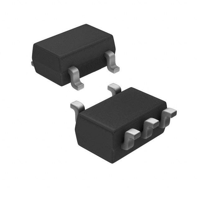
ICGOO电子元器件商城为您提供SN74LV06APWT由Texas Instruments设计生产,在icgoo商城现货销售,并且可以通过原厂、代理商等渠道进行代购。 SN74LV06APWT价格参考。Texas InstrumentsSN74LV06APWT封装/规格:逻辑 - 栅极和逆变器, Inverter IC 6 Channel Open Drain 14-TSSOP。您可以下载SN74LV06APWT参考资料、Datasheet数据手册功能说明书,资料中有SN74LV06APWT 详细功能的应用电路图电压和使用方法及教程。
| 参数 | 数值 |
| 产品目录 | 集成电路 (IC) |
| 描述 | IC BUFF/DVR INV HEX W/OD 14TSSOP |
| 产品分类 | |
| 品牌 | Texas Instruments |
| 数据手册 | |
| 产品图片 |
|
| 产品型号 | SN74LV06APWT |
| rohs | 无铅 / 符合限制有害物质指令(RoHS)规范要求 |
| 产品系列 | 74LV |
| 不同V、最大CL时的最大传播延迟 | 7.5ns @ 5V,50pF |
| 供应商器件封装 | 14-TSSOP |
| 其它名称 | 296-28626-1 |
| 包装 | 剪切带 (CT) |
| 安装类型 | 表面贴装 |
| 封装/外壳 | 14-TSSOP(0.173",4.40mm 宽) |
| 工作温度 | -40°C ~ 85°C |
| 标准包装 | 1 |
| 特性 | 开路漏极 |
| 电压-电源 | 2 V ~ 5.5 V |
| 电流-输出高,低 | -,16mA |
| 电流-静态(最大值) | 20µA |
| 电路数 | 6 |
| 输入数 | 6 |
| 逻辑电平-低 | 0.5V |
| 逻辑电平-高 | 1.5V |
| 逻辑类型 |


- 商务部:美国ITC正式对集成电路等产品启动337调查
- 曝三星4nm工艺存在良率问题 高通将骁龙8 Gen1或转产台积电
- 太阳诱电将投资9.5亿元在常州建新厂生产MLCC 预计2023年完工
- 英特尔发布欧洲新工厂建设计划 深化IDM 2.0 战略
- 台积电先进制程称霸业界 有大客户加持明年业绩稳了
- 达到5530亿美元!SIA预计今年全球半导体销售额将创下新高
- 英特尔拟将自动驾驶子公司Mobileye上市 估值或超500亿美元
- 三星加码芯片和SET,合并消费电子和移动部门,撤换高东真等 CEO
- 三星电子宣布重大人事变动 还合并消费电子和移动部门
- 海关总署:前11个月进口集成电路产品价值2.52万亿元 增长14.8%


PDF Datasheet 数据手册内容提取
Product Sample & Technical Tools & Support & Folder Buy Documents Software Community SN54LV06A,SN74LV06A SCES336J–MAY2000–REVISEDJANUARY2016 SNx4LV06A Hex Inverter Buffers/Drivers With Open-Drain Outputs 1 Features 2 Applications • 2-Vto5.5-VV Operation • Servers 1 CC • Maxt of6.5nsat5V • TelecomInfrastructures pd • TypicalV (OutputGroundBounce) • TVSet-TopBoxes OLP <0.8VatVCC=3.3V,TA=25°C • UPS • TypicalVOHV(OutputVOH Undershoot) • Printers >2.3VatV =3.3V,T =25°C CC A • Elevators,andEscalators • OutputsareDisabledDuringPowerUp • EPOS,ECR,andCashDrawers andPowerDownWithInputsTiedtoV CC • Vending,Payment,CashMachines • SupportMixed-ModeVoltageOperation onAllPorts 3 Description • I SupportsLiveinsertion,PartialPowerDown off These hex inverter buffers/drivers are designed for 2- Mode,andBackDriveProtection Vto5.5-VV operation. CC • Latch-UpPerformanceExceeds100mA The SN74LV06A device performs the Boolean PerJESD78,ClassII functionY= Ainpositivelogic. • ESDProtectionExceedsJESD22 The open-drain output require pull-up resistors to – 2500-VHuman-BodyModel(A114-1) perform correctly and can be connected to other – 200-VMachineModel(A115-A) open-drain outputs to implement active-low wired-OR oractive-highwired-ANDfunctions. – 2000-VCharged-DeviceMode(C101) DeviceInformation(1) PARTNUMBER PACKAGE BODYSIZE(NOM) TVSOP(14) 3.60mmx4.40mm SOIC(14) 8.65mm×3.91mm SN74LV06A SOP(14) 10.30mmx5.30mm SSOP(14) 6.20mmx5.30mm TSSOP(14) 5.00mmx4.40mm (1) For all available packages, see the orderable addendum at theendofthedatasheet. SPACER SPACER SimplifiedSchematic A Y 1 An IMPORTANT NOTICE at the end of this data sheet addresses availability, warranty, changes, use in safety-critical applications, intellectualpropertymattersandotherimportantdisclaimers.PRODUCTIONDATA.
SN54LV06A,SN74LV06A SCES336J–MAY2000–REVISEDJANUARY2016 www.ti.com Table of Contents 1 Features.................................................................. 1 8 DetailedDescription.............................................. 7 2 Applications........................................................... 1 8.1 Overview...................................................................7 3 Description............................................................. 1 8.2 FunctionalBlockDiagram.........................................7 4 RevisionHistory..................................................... 2 8.3 FeatureDescription...................................................8 8.4 DeviceFunctionalModes..........................................8 5 PinConfigurationandFunctions......................... 3 9 ApplicationandImplementation.......................... 9 6 Specifications......................................................... 4 9.1 ApplicationInformation..............................................9 6.1 AbsoluteMaximumRatings......................................4 9.2 TypicalApplication ...................................................9 6.2 ESDRatings..............................................................4 10 PowerSupplyRecommendations..................... 10 6.3 RecommendedOperatingConditions.......................4 6.4 ThermalInformation..................................................5 11 Layout................................................................... 10 6.5 ElectricalCharacteristics...........................................5 11.1 LayoutGuidelines.................................................10 6.6 SwitchingCharacteristics,V =2.5V±0.2V........5 11.2 LayoutExample....................................................10 CC 6.7 SwitchingCharacteristics,V =3.3V±0.3V........5 12 DeviceandDocumentationSupport................. 11 CC 6.8 SwitchingCharacteristics,V =5V±0.5V...........6 12.1 RelatedLinks........................................................11 CC 6.9 NoiseCharacteristics................................................6 12.2 Trademarks...........................................................11 6.10 OperatingCharacteristics........................................6 12.3 ElectrostaticDischargeCaution............................11 6.11 TypicalCharacteristics............................................6 12.4 Glossary................................................................11 7 ParameterMeasurementInformation..................7 13 Mechanical,Packaging,andOrderable Information........................................................... 11 4 Revision History ChangesfromRevisionI(February2015)toRevisionJ Page • AddedT JunctiontemperaturetotheAbsoluteMaximumRatings(1)table.......................................................................... 4 J • ChangedFigure6 ................................................................................................................................................................ 10 ChangesfromRevisionH(April2005)toRevisionI Page • AddedESDRatingstable,FeatureDescriptionsection,DeviceFunctionalModes,ApplicationandImplementation section,PowerSupplyRecommendationssection,Layoutsection,DeviceandDocumentationSupportsection,and Mechanical,Packaging,andOrderableInformationsection. ................................................................................................ 1 • Changeddatasheettitle......................................................................................................................................................... 1 2 SubmitDocumentationFeedback Copyright©2000–2016,TexasInstrumentsIncorporated ProductFolderLinks:SN54LV06A SN74LV06A
SN54LV06A,SN74LV06A www.ti.com SCES336J–MAY2000–REVISEDJANUARY2016 5 Pin Configuration and Functions (TOPVIEW) (TOPVIEW) NC - No internal connection PinFunctions PIN I/O DESCRIPTION NO. NAME 1 1A I Input1 2 1Y O Output1 3 2A I Input2 4 2Y O Output2 5 3A I Input3 6 3Y O Output3 7 GND GND GroundPin 8 4Y O Output4 9 4A I Input4 10 5Y O Output5 11 5A I Input5 12 6Y O Output6 13 6A I Input6 14 V — PowerPin CC Copyright©2000–2016,TexasInstrumentsIncorporated SubmitDocumentationFeedback 3 ProductFolderLinks:SN54LV06A SN74LV06A
SN54LV06A,SN74LV06A SCES336J–MAY2000–REVISEDJANUARY2016 www.ti.com 6 Specifications 6.1 Absolute Maximum Ratings(1) overoperatingfree-airtemperaturerange(unlessotherwisenoted) MIN MAX UNIT VCC Supplyvoltagerange –0.5 7 V VI Inputvoltagerange(2) –0.5 7 V VO Voltagerangeappliedtoanyoutputinthehigh-impedanceorpower-offstate(2) –0.5 7 V IIK Inputclampcurrent VI<0 –20 mA IOK Outputclampcurrent VO<0 –50 mA IO Continuousoutputcurrent VO=0toVCC –35 mA ContinuouscurrentthroughVCCorGND ±50 mA Tstg Storagetemperaturerange –65 150 °C TJ JunctionTemperature 150 °C (1) StressesbeyondthoselistedunderAbsoluteMaximumRatingsmaycausepermanentdamagetothedevice.Thesearestressratings only,andfunctionaloperationofthedeviceattheseoranyotherconditionsbeyondthoseindicatedunderRecommendedOperating Conditionsisnotimplied.Exposuretoabsolute-maximum-ratedconditionsforextendedperiodsmayaffectdevicereliability. (2) Theinputandoutputnegative-voltageratingsmaybeexceedediftheinputandoutputcurrentratingsareobserved. 6.2 ESD Ratings VALUE UNIT Human-bodymodel(HBM),perANSI/ESDA/JEDECJS-001(1) ±2500 V(ESD) Electrostaticdischarge Charged-devicemodel(CDM),perJEDECspecificationJESD22- V C101(2) ±2000 (1) JEDECdocumentJEP155statesthat500-VHBMallowssafemanufacturingwithastandardESDcontrolprocess.Manufacturingwith lessthan500-VHBMispossiblewiththenecessaryprecautions. (2) JEDECdocumentJEP157statesthat250-VCDMallowssafemanufacturingwithastandardESDcontrolprocess.Manufacturingwith lessthan250-VCDMispossiblewiththenecessaryprecautions. 6.3 Recommended Operating Conditions overoperatingfree-airtemperaturerange(unlessotherwisenoted)(1) SN54LV06A(2) SN74LV06A UNIT MIN MAX MIN MAX VCC Supplyvoltage 2 2 5.5 V VCC=2V .5 1.5 VCC=2.3Vto2.7V VCC×0.7 VCC×0.7 VIH Highlevelinputvoltage V VCC=3Vto3.6V VCC×0.7 VCC×0.7 VCC=4.5Vto5.5V VCC×0.7 VCC×0.7 VCC=2V 0.5 0.5 VCC=2.3Vto2.7V VCC×0.3 VCC×0.3 VIL Lowlevelinputvoltage V VCC=3Vto3.6V VCC×0.3 VCC×0.3 VCC=4.5Vto5.5V VCC×0.3 VCC×0.3 VI Inputvoltage 0 5.5 0 5.5 V VO Outputvoltage 0 5.5 0 5.5 V VCC=2V 50 20 µA VCC=2.3Vto2.7V 2 2 IOL Lowleveloutputcurrent VCC=3Vto3.6V 8 8 mA VCC=4.5Vto5.5V 16 16 VCC=2.3Vto2.7V 200 200 Δt/Δv Inputtransitionriseandfallrate VCC=3Vto3.6V 100 100 ns/V VCC=4.5Vto5.5V 20 20 TA Operatingfree-airtemperature –55 125 –40 125 °C (1) AllunusedinputsofthedevicemustbeheldatV orGNDtoensureproperdeviceoperation.RefertotheTIapplicationreport, CC ImplicationsofSloworFloatingCMOSInputs(SCBA004). (2) ProductPreview. 4 SubmitDocumentationFeedback Copyright©2000–2016,TexasInstrumentsIncorporated ProductFolderLinks:SN54LV06A SN74LV06A
SN54LV06A,SN74LV06A www.ti.com SCES336J–MAY2000–REVISEDJANUARY2016 6.4 Thermal Information SN74LV06A THERMALMETRIC(1) D DB DGV NS PW UNIT 14PINS 14PINS 14PINS 14PINS 14PINS R Junction-to-ambientthermalresistance 100.6 112.5 135.2 95.4 128.7 θJA R Junction-to-case(top)thermalresistance 51.8 65.0 57.9 52.9 57.2 θJC(top) R Junction-to-boardthermalresistance 54.9 59.9 68.3 51.2 70.7 °C/W θJB ψ Junction-to-topcharacterizationparameter 25.0 25.0 9.2 17.9 9.3 JT ψ Junction-to-boardcharacterizationparameter 54.7 59.3 67.6 53.8 70.0 JB (1) Formoreinformationabouttraditionalandnewthermalmetrics,seetheICPackageThermalMetricsapplicationreport(SPRA953). 6.5 Electrical Characteristics overrecommendedoperatingfree-airtemperaturerange(unlessotherwisenoted) –40°Cto85°C –40°Cto125°C SN74LV06A PARAMETER TESTCONDITIONS VCC SN74LV06A SN74LV06A UNIT MIN TYP MAX MIN TYP MAX IOL=50µA 2Vto5.5V 0.1 0.1 0.1 IOL=2mA 2.3V 0.4 0.4 0.4 VOL V IOL=8mA 3V 0.44 0.44 0.44 IOL=16mA 4.5V 0.55 0.55 0.55 II VI=5.5VorGND 0to5.5V ±1 ±1 ±1 µA IOH VI=VIL, VOH=VCC 5.5V ±2.5 ±2.5 ±2.5 µA ICC VI=VCCorGND, IO=0 5.5V 20 20 20 µA Ioff VIorVO=0to5.5V 0 5 5 5 µA Ci VI=VCCorGND 3.3V 1.6 1.6 1.6 pF 6.6 Switching Characteristics, V = 2.5 V ± 0.2 V CC overrecommendedoperatingfree-airtemperaturerange(unlessotherwisenoted)(seeFigure3) –40°Cto85°C –40°Cto125°C PARAMETER FROM TO LOAD TA=25°C SN74LV06A SN74LV06A UNIT (INPUT) (OUTPUT) CAPACITANCE MIN TYP MAX MIN MAX MIN MAX tPLH 5.4(1) 10.4(1) 1(1) 13(1) 1 14 tPHL A Y CL=15pF 7.2(1) 10.4(1) 1(1) 13(1) 1 14 ns tPLH A Y 9.7 15.2 1 18 1 19 CL=50pF ns tPHL A Y 9.3 15.2 1 18 1 19 (1) OnproductscomplianttoMIL-PRF-38535,thisparameterisnotproductiontested. 6.7 Switching Characteristics, V = 3.3 V ± 0.3 V CC overrecommendedoperatingfree-airtemperaturerange(unlessotherwisenoted)(seeFigure3) –40°Cto85°C –40°Cto125°C PARAMETER FROM TO LOAD TA=25°C SN74LV06A SN74LV06A UNIT (INPUT) (OUTPUT) CAPACITANCE MIN TYP MAX MIN MAX MIN MAX tPLH A Y 4.1(1) 7.1(1) 1(1) 8.5(1) 1 9.5 tPHL A Y CL=15pF 4.9(1) 7.1(1) 1(1) 8.5(1) 1 9.5 ns tPLH A Y 7.1 10.6 1 12 1 13 CL=50pF ns tPHL A Y 6.4 10.6 1 12 1 13 (1) OnproductscomplianttoMIL-PRF-38535,thisparameterisnotproductiontested. Copyright©2000–2016,TexasInstrumentsIncorporated SubmitDocumentationFeedback 5 ProductFolderLinks:SN54LV06A SN74LV06A
SN54LV06A,SN74LV06A SCES336J–MAY2000–REVISEDJANUARY2016 www.ti.com 6.8 Switching Characteristics, V = 5 V ± 0.5 V CC operatingfree-airtemperaturerange(unlessotherwisenoted)(seeFigure3) –40°Cto85°C –40°Cto125°C PARAMETER FROM TO LOAD TA=25°C SN74LV06A SN74LV06A UNIT (INPUT) (OUTPUT) CAPACITANCE MIN TYP MAX MIN MAX MIN MAX tPLH A Y 3(1) 5.5(1) 1(1) 6.5(1) 1 7 tPHL A Y CL=15pF 3.3(1) 5.5(1) 1(1) 6.5(1) 1 7 ns tPLH A Y 4.8 7.5 1 8.5 1 9 CL=50pF ns tPHL A Y 4.4 7.5 1 8.5 1 9 (1) OnproductscomplianttoMIL-PRF-38535,thisparameterisnotproductiontested. 6.9 Noise Characteristics(1) V =3.3V,C =50pF,T =25°C CC L A PARAMETER MIN TYP MAX UNIT V Quietoutput,maximumdynamicV 0.5 0.8 V OL(P) OL V Quietoutput,minimumdynamicVOL –0.1 –0.8 V OL(V) V Quietoutput,minimumdynamicV 3.3 V OH(V) OH V High-leveldynamicinputvoltage 2.31 V IH(D) V Low-leveldynamicinputvoltage 0.99 V IL(D) (1) Characteristicsareforsurface-mountpackagesonly. 6.10 Operating Characteristics T =25°C A PARAMETER TESTCONDITIONS V TYP UNIT CC 3.3V 2.6 C Powerdissipationcapacitance C =50pF, f=10MHz pF pd L 5V 4.7 6.11 Typical Characteristics 4 7 TPD in ns 3.5 6 3 5 2.5 PD (ms) 2 TPD (ns) 34 T 1.5 2 1 1 0.5 TPD in ns 0 0 0 1 2 3 4 5 6 -100 -50 Te0mperature (5q0C) 100 150 VCC (V) D002 D001 Figure2.TPDvsV at25°C Figure1.TPDvsTemperatureat5V CC 6 SubmitDocumentationFeedback Copyright©2000–2016,TexasInstrumentsIncorporated ProductFolderLinks:SN54LV06A SN74LV06A
SN54LV06A,SN74LV06A www.ti.com SCES336J–MAY2000–REVISEDJANUARY2016 7 Parameter Measurement Information VCC VCC RL=1kΩ Input 50%VCC 50%VCC 0V FromOutput Test UnderTest Point tPHL tPLH CL ≈VCC (seeNoteA) Output 50%VCC VOL+0.3V VOL LOADCIRCUITFOR VOLTAGEWAVEFORMS OPEN-DRAINOUTPUTS PROPAGATIONDELAYTIMES A. C includesprobeandjigcapacitance. L B. Allinputpulsesaresuppliedbygeneratorshavingthefollowingcharacteristics:PRR≤1MHz,Z =50Ω,t ≤3ns, O r t ≤3ns. f C. Theoutputsaremeasuredoneatatime,withoneinputtransitionpermeasurement. Figure3. LoadCircuitandVoltageWaveforms 8 Detailed Description 8.1 Overview Thesehexinverterbuffers/driversaredesignedfor2-Vto5.5-VV operation. CC TheSN74LV06AdeviceperformstheBooleanfunctionY= Ainpositivelogic. The open-drain output require pull-up resistors to perform correctly and can be connected to other open-drain outputstoimplementactive-lowwired-ORoractive-highwired-ANDfunctions. These devices are fully specified for partial-power-down applications using I . The I circuitry disables the off off outputs,preventingdamagingcurrentback-flowthroughthedeviceswhentheyarepowereddown. 8.2 Functional Block Diagram A Y Figure4. LogicDiagram(PositiveLogic) Copyright©2000–2016,TexasInstrumentsIncorporated SubmitDocumentationFeedback 7 ProductFolderLinks:SN54LV06A SN74LV06A
SN54LV06A,SN74LV06A SCES336J–MAY2000–REVISEDJANUARY2016 www.ti.com 8.3 Feature Description • Wideoperatingvoltagerange – Operatesfrom2Vto5.5V • Allowsupordownvoltagetranslation – Inputsandoutputsacceptvoltagesto5.5V • I feature off – AllowsvoltagesontheinputsandoutputswhenV is0V CC 8.4 Device Functional Modes Table1.FunctionTable (EachInverter) INPUT OUTPUT A Y H L L H 8 SubmitDocumentationFeedback Copyright©2000–2016,TexasInstrumentsIncorporated ProductFolderLinks:SN54LV06A SN74LV06A
SN54LV06A,SN74LV06A www.ti.com SCES336J–MAY2000–REVISEDJANUARY2016 9 Application and Implementation NOTE Information in the following applications sections is not part of the TI component specification, and TI does not warrant its accuracy or completeness. TI’s customers are responsible for determining suitability of components for their purposes. Customers should validateandtesttheirdesignimplementationtoconfirmsystemfunctionality. 9.1 Application Information The SN74LV06A is a low drive Open drain CMOS device that can be used for a multitude of buffer type functions.Theinputsare5.5Vtolerantandtheoutputsopendrainand5.5Vtolerantallowingittotranslateupto 5.5VordowntoanyothervoltagebetweenGNDand5.5V. 9.2 Typical Application Buffer Function Basic LED Driver VPU VPU Wired OR uC or Logic LV06A uC or Logic uC or Logic LV06A uC or Logic LV06A Figure5. TypicalApplicationSchematic 9.2.1 DesignRequirements This device uses CMOS technology and is open drain so it has low output drive only. Care should be taken to avoid bus contention because it can drive currents that would exceed maximum limits. The parallel output drive cancreatefastedgesintolightloadssoroutingandloadconditionsshouldbeconsideredtopreventringing. 9.2.2 DetailedDesignProcedure 1. RecommendedInputConditions: – Forrisetimeandfalltimespecifications,see Δt/ΔVintheRecommendedOperatingConditions table. – Forspecifiedhighandlowlevels,seeV andV intheRecommendedOperatingConditionstable. IH IL – Inputsareovervoltagetolerantallowingthemtogoashighas5.5VatanyvalidV . CC 2. RecommendedOutputConditions: – Loadcurrentsshouldnotexceed35mAperoutputand50mAtotalforthepart. Copyright©2000–2016,TexasInstrumentsIncorporated SubmitDocumentationFeedback 9 ProductFolderLinks:SN54LV06A SN74LV06A
SN54LV06A,SN74LV06A SCES336J–MAY2000–REVISEDJANUARY2016 www.ti.com Typical Application (continued) 9.2.3 ApplicationCurves 3.5 VOUT input low 3 VOUT input high 2.5 2 V) T ( 1.5 U O V 1 0.5 0 -0.5 0 1 2 3 4 VCC (V) D003 Figure6.OutputDuringPowerUpwith4kPull-upat3.3V 10 Power Supply Recommendations The power supply can be any voltage between the MIN and MAX supply voltage rating located in the Recommended Operating Conditions. Each V terminal should have a good bypass capacitor to prevent power CC disturbance. For devices with a single supply, a 0.1 μF capacitor is recommended. If there are multiple V CC terminalsthen0.01μFor0.022μFcapacitorisrecommendedforeachpowerterminal.Itisacceptabletoparallel multiple bypass capacitors to reject different frequencies of noise. 0.1 μF and 1 μF capacitors are commonly used in parallel. The bypass capacitor should be installed as close to the power terminal as possible for best results. 11 Layout 11.1 Layout Guidelines Whenusingmultiplebitlogicdevices,inputsshouldnotfloat. In many cases, functions or parts of functions of digital logic devices are unused, for example, when only two inputs of a triple-input AND gate are used or only 3 of the 4 buffer gates are used. Such input pins should not be left unconnected because the undefined voltages at the outside connections result in undefined operational states. Specified below are the rules that must be observed under all circumstances. All unused inputs of digital logic devices must be connected to a high or low bias to prevent them from floating. The logic level that should be applied to any particular unused input depends on the function of the device. Generally they will be tied to GND or V whichever make more sense or is more convenient. It is generally OK to float outputs unless the CC partisatransceiver. 11.2 Layout Example V cc Input Unused Input Output Unused Input Output Input Figure7. LayoutDiagram 10 SubmitDocumentationFeedback Copyright©2000–2016,TexasInstrumentsIncorporated ProductFolderLinks:SN54LV06A SN74LV06A
SN54LV06A,SN74LV06A www.ti.com SCES336J–MAY2000–REVISEDJANUARY2016 12 Device and Documentation Support 12.1 Related Links The table below lists quick access links. Categories include technical documents, support and community resources,toolsandsoftware,andquickaccesstosampleorbuy. Table2.RelatedLinks TECHNICAL TOOLS& SUPPORT& PARTS PRODUCTFOLDER SAMPLE&BUY DOCUMENTS SOFTWARE COMMUNITY SN54LV06A Clickhere Clickhere Clickhere Clickhere Clickhere SN74LV06A Clickhere Clickhere Clickhere Clickhere Clickhere 12.2 Trademarks Alltrademarksarethepropertyoftheirrespectiveowners. 12.3 Electrostatic Discharge Caution Thesedeviceshavelimitedbuilt-inESDprotection.Theleadsshouldbeshortedtogetherorthedeviceplacedinconductivefoam duringstorageorhandlingtopreventelectrostaticdamagetotheMOSgates. 12.4 Glossary SLYZ022—TIGlossary. Thisglossarylistsandexplainsterms,acronyms,anddefinitions. 13 Mechanical, Packaging, and Orderable Information The following pages include mechanical, packaging, and orderable information. This information is the most current data available for the designated devices. This data is subject to change without notice and revision of thisdocument.Forbrowser-basedversionsofthisdatasheet,refertotheleft-handnavigation. Copyright©2000–2016,TexasInstrumentsIncorporated SubmitDocumentationFeedback 11 ProductFolderLinks:SN54LV06A SN74LV06A
PACKAGE OPTION ADDENDUM www.ti.com 24-Aug-2018 PACKAGING INFORMATION Orderable Device Status Package Type Package Pins Package Eco Plan Lead/Ball Finish MSL Peak Temp Op Temp (°C) Device Marking Samples (1) Drawing Qty (2) (6) (3) (4/5) SN74LV06AD ACTIVE SOIC D 14 50 Green (RoHS CU NIPDAU Level-1-260C-UNLIM -40 to 125 LV06A & no Sb/Br) SN74LV06ADBR ACTIVE SSOP DB 14 2000 Green (RoHS CU NIPDAU Level-1-260C-UNLIM -40 to 125 LV06A & no Sb/Br) SN74LV06ADGVR ACTIVE TVSOP DGV 14 2000 Green (RoHS CU NIPDAU Level-1-260C-UNLIM -40 to 125 LV06A & no Sb/Br) SN74LV06ADR ACTIVE SOIC D 14 2500 Green (RoHS CU NIPDAU Level-1-260C-UNLIM -40 to 125 LV06A & no Sb/Br) SN74LV06ADRE4 ACTIVE SOIC D 14 2500 Green (RoHS CU NIPDAU Level-1-260C-UNLIM -40 to 125 LV06A & no Sb/Br) SN74LV06ANSR ACTIVE SO NS 14 2000 Green (RoHS CU NIPDAU Level-1-260C-UNLIM -40 to 125 74LV06A & no Sb/Br) SN74LV06APW ACTIVE TSSOP PW 14 90 Green (RoHS CU NIPDAU Level-1-260C-UNLIM -40 to 125 LV06A & no Sb/Br) SN74LV06APWR ACTIVE TSSOP PW 14 2000 Green (RoHS CU NIPDAU Level-1-260C-UNLIM -40 to 125 LV06A & no Sb/Br) SN74LV06APWRG4 ACTIVE TSSOP PW 14 2000 Green (RoHS CU NIPDAU Level-1-260C-UNLIM -40 to 125 LV06A & no Sb/Br) SN74LV06APWT ACTIVE TSSOP PW 14 250 Green (RoHS CU NIPDAU Level-1-260C-UNLIM -40 to 125 LV06A & no Sb/Br) (1) The marketing status values are defined as follows: ACTIVE: Product device recommended for new designs. LIFEBUY: TI has announced that the device will be discontinued, and a lifetime-buy period is in effect. NRND: Not recommended for new designs. Device is in production to support existing customers, but TI does not recommend using this part in a new design. PREVIEW: Device has been announced but is not in production. Samples may or may not be available. OBSOLETE: TI has discontinued the production of the device. (2) RoHS: TI defines "RoHS" to mean semiconductor products that are compliant with the current EU RoHS requirements for all 10 RoHS substances, including the requirement that RoHS substance do not exceed 0.1% by weight in homogeneous materials. Where designed to be soldered at high temperatures, "RoHS" products are suitable for use in specified lead-free processes. TI may reference these types of products as "Pb-Free". RoHS Exempt: TI defines "RoHS Exempt" to mean products that contain lead but are compliant with EU RoHS pursuant to a specific EU RoHS exemption. Green: TI defines "Green" to mean the content of Chlorine (Cl) and Bromine (Br) based flame retardants meet JS709B low halogen requirements of <=1000ppm threshold. Antimony trioxide based flame retardants must also meet the <=1000ppm threshold requirement. (3) MSL, Peak Temp. - The Moisture Sensitivity Level rating according to the JEDEC industry standard classifications, and peak solder temperature. Addendum-Page 1
PACKAGE OPTION ADDENDUM www.ti.com 24-Aug-2018 (4) There may be additional marking, which relates to the logo, the lot trace code information, or the environmental category on the device. (5) Multiple Device Markings will be inside parentheses. Only one Device Marking contained in parentheses and separated by a "~" will appear on a device. If a line is indented then it is a continuation of the previous line and the two combined represent the entire Device Marking for that device. (6) Lead/Ball Finish - Orderable Devices may have multiple material finish options. Finish options are separated by a vertical ruled line. Lead/Ball Finish values may wrap to two lines if the finish value exceeds the maximum column width. Important Information and Disclaimer:The information provided on this page represents TI's knowledge and belief as of the date that it is provided. TI bases its knowledge and belief on information provided by third parties, and makes no representation or warranty as to the accuracy of such information. Efforts are underway to better integrate information from third parties. TI has taken and continues to take reasonable steps to provide representative and accurate information but may not have conducted destructive testing or chemical analysis on incoming materials and chemicals. TI and TI suppliers consider certain information to be proprietary, and thus CAS numbers and other limited information may not be available for release. In no event shall TI's liability arising out of such information exceed the total purchase price of the TI part(s) at issue in this document sold by TI to Customer on an annual basis. Addendum-Page 2
PACKAGE MATERIALS INFORMATION www.ti.com 20-Dec-2018 TAPE AND REEL INFORMATION *Alldimensionsarenominal Device Package Package Pins SPQ Reel Reel A0 B0 K0 P1 W Pin1 Type Drawing Diameter Width (mm) (mm) (mm) (mm) (mm) Quadrant (mm) W1(mm) SN74LV06ADGVR TVSOP DGV 14 2000 330.0 12.4 6.8 4.0 1.6 8.0 12.0 Q1 SN74LV06ADR SOIC D 14 2500 330.0 16.4 6.5 9.0 2.1 8.0 16.0 Q1 SN74LV06ANSR SO NS 14 2000 330.0 16.4 8.2 10.5 2.5 12.0 16.0 Q1 SN74LV06APWR TSSOP PW 14 2000 330.0 12.4 6.9 5.6 1.6 8.0 12.0 Q1 SN74LV06APWT TSSOP PW 14 250 330.0 12.4 6.9 5.6 1.6 8.0 12.0 Q1 PackMaterials-Page1
PACKAGE MATERIALS INFORMATION www.ti.com 20-Dec-2018 *Alldimensionsarenominal Device PackageType PackageDrawing Pins SPQ Length(mm) Width(mm) Height(mm) SN74LV06ADGVR TVSOP DGV 14 2000 367.0 367.0 35.0 SN74LV06ADR SOIC D 14 2500 367.0 367.0 38.0 SN74LV06ANSR SO NS 14 2000 367.0 367.0 38.0 SN74LV06APWR TSSOP PW 14 2000 367.0 367.0 35.0 SN74LV06APWT TSSOP PW 14 250 367.0 367.0 35.0 PackMaterials-Page2
None
MECHANICAL DATA MPDS006C – FEBRUARY 1996 – REVISED AUGUST 2000 DGV (R-PDSO-G**) PLASTIC SMALL-OUTLINE 24 PINS SHOWN 0,23 0,40 0,07 M 0,13 24 13 0,16 NOM 4,50 6,60 4,30 6,20 Gage Plane 0,25 0°–(cid:1)8° 0,75 1 12 0,50 A Seating Plane 0,15 1,20 MAX 0,08 0,05 PINS ** 14 16 20 24 38 48 56 DIM A MAX 3,70 3,70 5,10 5,10 7,90 9,80 11,40 A MIN 3,50 3,50 4,90 4,90 7,70 9,60 11,20 4073251/E 08/00 NOTES: A. All linear dimensions are in millimeters. B. This drawing is subject to change without notice. C. Body dimensions do not include mold flash or protrusion, not to exceed 0,15 per side. D. Falls within JEDEC: 24/48 Pins – MO-153 14/16/20/56 Pins – MO-194 • POST OFFICE BOX 655303 DALLAS, TEXAS 75265
None
None
None
None
MECHANICAL DATA MSSO002E – JANUARY 1995 – REVISED DECEMBER 2001 DB (R-PDSO-G**) PLASTIC SMALL-OUTLINE 28 PINS SHOWN 0,38 0,65 0,15 M 0,22 28 15 0,25 0,09 5,60 8,20 5,00 7,40 Gage Plane 1 14 0,25 A 0°–(cid:1)8° 0,95 0,55 Seating Plane 2,00 MAX 0,05 MIN 0,10 PINS ** 14 16 20 24 28 30 38 DIM A MAX 6,50 6,50 7,50 8,50 10,50 10,50 12,90 A MIN 5,90 5,90 6,90 7,90 9,90 9,90 12,30 4040065/E 12/01 NOTES: A. All linear dimensions are in millimeters. B. This drawing is subject to change without notice. C. Body dimensions do not include mold flash or protrusion not to exceed 0,15. D. Falls within JEDEC MO-150 • POST OFFICE BOX 655303 DALLAS, TEXAS 75265
IMPORTANTNOTICEANDDISCLAIMER TIPROVIDESTECHNICALANDRELIABILITYDATA(INCLUDINGDATASHEETS),DESIGNRESOURCES(INCLUDINGREFERENCE DESIGNS),APPLICATIONOROTHERDESIGNADVICE,WEBTOOLS,SAFETYINFORMATION,ANDOTHERRESOURCES“ASIS” ANDWITHALLFAULTS,ANDDISCLAIMSALLWARRANTIES,EXPRESSANDIMPLIED,INCLUDINGWITHOUTLIMITATIONANY IMPLIEDWARRANTIESOFMERCHANTABILITY,FITNESSFORAPARTICULARPURPOSEORNON-INFRINGEMENTOFTHIRD PARTYINTELLECTUALPROPERTYRIGHTS. TheseresourcesareintendedforskilleddevelopersdesigningwithTIproducts.Youaresolelyresponsiblefor(1)selectingtheappropriate TIproductsforyourapplication,(2)designing,validatingandtestingyourapplication,and(3)ensuringyourapplicationmeetsapplicable standards,andanyothersafety,security,orotherrequirements.Theseresourcesaresubjecttochangewithoutnotice.TIgrantsyou permissiontousetheseresourcesonlyfordevelopmentofanapplicationthatusestheTIproductsdescribedintheresource.Other reproductionanddisplayoftheseresourcesisprohibited.NolicenseisgrantedtoanyotherTIintellectualpropertyrightortoanythird partyintellectualpropertyright.TIdisclaimsresponsibilityfor,andyouwillfullyindemnifyTIanditsrepresentativesagainst,anyclaims, damages,costs,losses,andliabilitiesarisingoutofyouruseoftheseresources. TI’sproductsareprovidedsubjecttoTI’sTermsofSale(www.ti.com/legal/termsofsale.html)orotherapplicabletermsavailableeitheron ti.comorprovidedinconjunctionwithsuchTIproducts.TI’sprovisionoftheseresourcesdoesnotexpandorotherwisealterTI’sapplicable warrantiesorwarrantydisclaimersforTIproducts. MailingAddress:TexasInstruments,PostOfficeBox655303,Dallas,Texas75265 Copyright©2019,TexasInstrumentsIncorporated