ICGOO在线商城 > 集成电路(IC) > 逻辑 - 缓冲器,驱动器,接收器,收发器 > SN74LS540DBR

 Datasheet下载
- 型号: SN74LS540DBR
- 制造商: Texas Instruments
- 库位|库存: xxxx|xxxx
- 要求:
| 数量阶梯 | 香港交货 | 国内含税 |
| +xxxx | $xxxx | ¥xxxx |
查看当月历史价格
查看今年历史价格
SN74LS540DBR产品简介:
ICGOO电子元器件商城为您提供SN74LS540DBR由Texas Instruments设计生产,在icgoo商城现货销售,并且可以通过原厂、代理商等渠道进行代购。 SN74LS540DBR价格参考。Texas InstrumentsSN74LS540DBR封装/规格:逻辑 - 缓冲器,驱动器,接收器,收发器, Buffer, Inverting 1 Element 8 Bit per Element 3-State Output 20-SSOP。您可以下载SN74LS540DBR参考资料、Datasheet数据手册功能说明书,资料中有SN74LS540DBR 详细功能的应用电路图电压和使用方法及教程。
| 参数 | 数值 |
| 产品目录 | 集成电路 (IC)半导体 |
| 描述 | IC INVERTER 8-INPUT 20SSOP缓冲器和线路驱动器 Octal Buff/Line Drvr W/3-State Otpt |
| 产品分类 | |
| 品牌 | Texas Instruments |
| 产品手册 | |
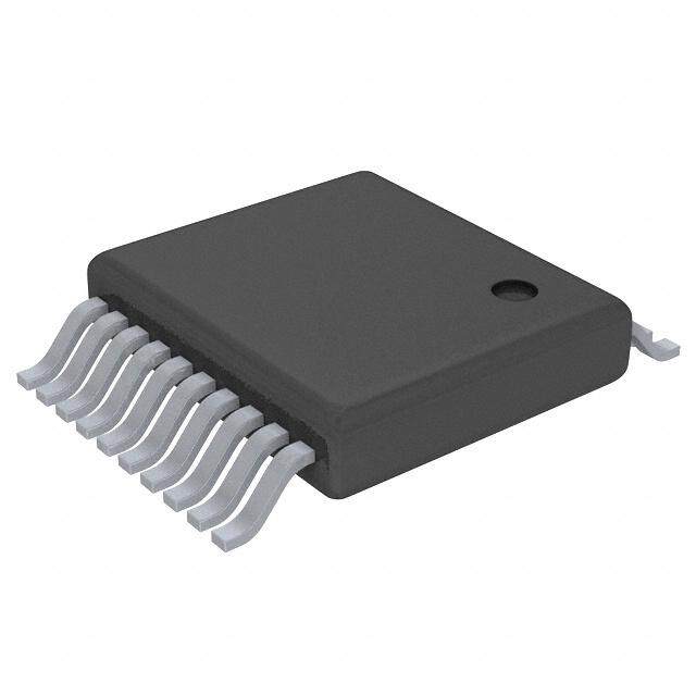
| 产品图片 |
|
| rohs | 符合RoHS无铅 / 符合限制有害物质指令(RoHS)规范要求 |
| 产品系列 | 逻辑集成电路,缓冲器和线路驱动器,Texas Instruments SN74LS540DBR74LS |
| 数据手册 | |
| 产品型号 | SN74LS540DBR |
| 不同V、最大CL时的最大传播延迟 | 15ns @ 5V,45pF |
| 产品种类 | Logic - Buffers, Drivers, and Transceivers |
| 传播延迟时间 | 15 ns at 5 V |
| 低电平输出电流 | 24 mA |
| 供应商器件封装 | 20-SSOP |
| 元件数 | 1 |
| 其它名称 | 296-31858-1 |
| 包装 | 剪切带 (CT) |
| 单位重量 | 156.700 mg |
| 商标 | Texas Instruments |
| 安装类型 | 表面贴装 |
| 安装风格 | SMD/SMT |
| 封装 | Reel |
| 封装/外壳 | 20-SSOP(0.209",5.30mm 宽) |
| 封装/箱体 | SSOP-20 |
| 工作温度 | 0°C ~ 70°C |
| 工厂包装数量 | 2000 |
| 最大工作温度 | + 70 C |
| 最小工作温度 | 0 C |
| 极性 | Inverting |
| 标准包装 | 1 |
| 每元件位数 | 8 |
| 每芯片的通道数量 | 8 |
| 特性 | 三态 |
| 电压-电源 | 4.75 V ~ 5.25 V |
| 电流-输出高,低 | 15mA,24mA |
| 电流-静态(最大值) | - |
| 电源电压-最大 | 5.25 V |
| 电源电压-最小 | 4.75 V |
| 电源电流 | 0.045 mA |
| 电路数 | 1 |
| 系列 | SN74LS540 |
| 输入数 | 8 |
| 输入线路数量 | 8 |
| 输出类型 | 3-State |
| 输出线路数量 | 8 |
| 逻辑电平-低 | 0.6V |
| 逻辑电平-高 | 2V |
| 逻辑类型 | 缓冲器/线路驱动器, 反相 |
| 逻辑系列 | LS |
| 高电平输出电流 | - 15 mA |


- 商务部:美国ITC正式对集成电路等产品启动337调查
- 曝三星4nm工艺存在良率问题 高通将骁龙8 Gen1或转产台积电
- 太阳诱电将投资9.5亿元在常州建新厂生产MLCC 预计2023年完工
- 英特尔发布欧洲新工厂建设计划 深化IDM 2.0 战略
- 台积电先进制程称霸业界 有大客户加持明年业绩稳了
- 达到5530亿美元!SIA预计今年全球半导体销售额将创下新高
- 英特尔拟将自动驾驶子公司Mobileye上市 估值或超500亿美元
- 三星加码芯片和SET,合并消费电子和移动部门,撤换高东真等 CEO
- 三星电子宣布重大人事变动 还合并消费电子和移动部门
- 海关总署:前11个月进口集成电路产品价值2.52万亿元 增长14.8%


PDF Datasheet 数据手册内容提取
(cid:1)(cid:2)(cid:3)(cid:4)(cid:5)(cid:1)(cid:3)(cid:4)(cid:6)(cid:7) (cid:1)(cid:2)(cid:3)(cid:4)(cid:5)(cid:1)(cid:3)(cid:4)(cid:8)(cid:7) (cid:1)(cid:2)(cid:9)(cid:4)(cid:5)(cid:1)(cid:3)(cid:4)(cid:6)(cid:7) (cid:1)(cid:2)(cid:9)(cid:4)(cid:5)(cid:1)(cid:3)(cid:4)(cid:8) (cid:10)(cid:11)(cid:12)(cid:13)(cid:5) (cid:14)(cid:15)(cid:16)(cid:16)(cid:17)(cid:18)(cid:1) (cid:13)(cid:2)(cid:19) (cid:5)(cid:20)(cid:2)(cid:17) (cid:19)(cid:18)(cid:20)(cid:21)(cid:17)(cid:18)(cid:1) (cid:22)(cid:20)(cid:12)(cid:23) (cid:24)(cid:25)(cid:1)(cid:12)(cid:13)(cid:12)(cid:17) (cid:10)(cid:15)(cid:12)(cid:26)(cid:15)(cid:12)(cid:1) SDLS180 − AUGUST 1979 − REVISED MARCH 1988 (cid:26)(cid:18)(cid:10)(cid:19)(cid:15)(cid:11)(cid:12)(cid:20)(cid:10)(cid:2) (cid:19)(cid:13)(cid:12)(cid:13) (cid:27)(cid:28)(cid:29)(cid:30)(cid:31)!"#(cid:27)(cid:30)(cid:28) (cid:27)$ %&(cid:31)(cid:31)’(cid:28)# "$ (cid:30)(cid:29) (&)*(cid:27)%"#(cid:27)(cid:30)(cid:28) +"#’, Copyright 1988, Texas Instruments Incorporated (cid:26)(cid:31)(cid:30)+&%#$ %(cid:30)(cid:28)(cid:29)(cid:30)(cid:31)! #(cid:30) $(’%(cid:27)(cid:29)(cid:27)%"#(cid:27)(cid:30)(cid:28)$ (’(cid:31) #-’ #’(cid:31)!$ (cid:30)(cid:29) (cid:12)’."$ (cid:20)(cid:28)$#(cid:31)&!’(cid:28)#$ $#"(cid:28)+"(cid:31)+ /"(cid:31)(cid:31)"(cid:28)#0, (cid:26)(cid:31)(cid:30)+&%#(cid:27)(cid:30)(cid:28) ((cid:31)(cid:30)%’$$(cid:27)(cid:28)1 +(cid:30)’$ (cid:28)(cid:30)# (cid:28)’%’$$"(cid:31)(cid:27)*0 (cid:27)(cid:28)%*&+’ #’$#(cid:27)(cid:28)1 (cid:30)(cid:29) "** ("(cid:31)"!’#’(cid:31)$, POST OFFICE BOX 655303 • DALLAS, TEXAS 75265 1
(cid:1)(cid:2)(cid:3)(cid:4)(cid:5)(cid:1)(cid:3)(cid:4)(cid:6)(cid:7) (cid:1)(cid:2)(cid:3)(cid:4)(cid:5)(cid:1)(cid:3)(cid:4)(cid:8)(cid:7) (cid:1)(cid:2)(cid:9)(cid:4)(cid:5)(cid:1)(cid:3)(cid:4)(cid:6)(cid:7) (cid:1)(cid:2)(cid:9)(cid:4)(cid:5)(cid:1)(cid:3)(cid:4)(cid:8) (cid:10)(cid:11)(cid:12)(cid:13)(cid:5) (cid:14)(cid:15)(cid:16)(cid:16)(cid:17)(cid:18)(cid:1) (cid:13)(cid:2)(cid:19) (cid:5)(cid:20)(cid:2)(cid:17) (cid:19)(cid:18)(cid:20)(cid:21)(cid:17)(cid:18)(cid:1) (cid:22)(cid:20)(cid:12)(cid:23) (cid:24)(cid:25)(cid:1)(cid:12)(cid:13)(cid:12)(cid:17) (cid:10)(cid:15)(cid:12)(cid:26)(cid:15)(cid:12)(cid:1) SDLS180 − AUGUST 1979 − REVISED MARCH 1988 2 POST OFFICE BOX 655303 • DALLAS, TEXAS 75265
(cid:1)(cid:2)(cid:3)(cid:4)(cid:5)(cid:1)(cid:3)(cid:4)(cid:6)(cid:7) (cid:1)(cid:2)(cid:3)(cid:4)(cid:5)(cid:1)(cid:3)(cid:4)(cid:8)(cid:7) (cid:1)(cid:2)(cid:9)(cid:4)(cid:5)(cid:1)(cid:3)(cid:4)(cid:6)(cid:7) (cid:1)(cid:2)(cid:9)(cid:4)(cid:5)(cid:1)(cid:3)(cid:4)(cid:8) (cid:10)(cid:11)(cid:12)(cid:13)(cid:5) (cid:14)(cid:15)(cid:16)(cid:16)(cid:17)(cid:18)(cid:1) (cid:13)(cid:2)(cid:19) (cid:5)(cid:20)(cid:2)(cid:17) (cid:19)(cid:18)(cid:20)(cid:21)(cid:17)(cid:18)(cid:1) (cid:22)(cid:20)(cid:12)(cid:23) (cid:24)(cid:25)(cid:1)(cid:12)(cid:13)(cid:12)(cid:17) (cid:10)(cid:15)(cid:12)(cid:26)(cid:15)(cid:12)(cid:1) SDLS180 − AUGUST 1979 − REVISED MARCH 1988 POST OFFICE BOX 655303 • DALLAS, TEXAS 75265 3
(cid:1)(cid:2)(cid:3)(cid:4)(cid:5)(cid:1)(cid:3)(cid:4)(cid:6)(cid:7) (cid:1)(cid:2)(cid:3)(cid:4)(cid:5)(cid:1)(cid:3)(cid:4)(cid:8)(cid:7) (cid:1)(cid:2)(cid:9)(cid:4)(cid:5)(cid:1)(cid:3)(cid:4)(cid:6)(cid:7) (cid:1)(cid:2)(cid:9)(cid:4)(cid:5)(cid:1)(cid:3)(cid:4)(cid:8) (cid:10)(cid:11)(cid:12)(cid:13)(cid:5) (cid:14)(cid:15)(cid:16)(cid:16)(cid:17)(cid:18)(cid:1) (cid:13)(cid:2)(cid:19) (cid:5)(cid:20)(cid:2)(cid:17) (cid:19)(cid:18)(cid:20)(cid:21)(cid:17)(cid:18)(cid:1) (cid:22)(cid:20)(cid:12)(cid:23) (cid:24)(cid:25)(cid:1)(cid:12)(cid:13)(cid:12)(cid:17) (cid:10)(cid:15)(cid:12)(cid:26)(cid:15)(cid:12)(cid:1) SDLS180 − AUGUST 1979 − REVISED MARCH 1988 4 POST OFFICE BOX 655303 • DALLAS, TEXAS 75265
PACKAGE OPTION ADDENDUM www.ti.com 24-Aug-2018 PACKAGING INFORMATION Orderable Device Status Package Type Package Pins Package Eco Plan Lead/Ball Finish MSL Peak Temp Op Temp (°C) Device Marking Samples (1) Drawing Qty (2) (6) (3) (4/5) 84155012A ACTIVE LCCC FK 20 1 TBD POST-PLATE N / A for Pkg Type -55 to 125 84155012A SNJ54LS 540FK 8415501RA ACTIVE CDIP J 20 1 TBD A42 N / A for Pkg Type -55 to 125 8415501RA SNJ54LS540J 8415501RA ACTIVE CDIP J 20 1 TBD A42 N / A for Pkg Type -55 to 125 8415501RA SNJ54LS540J 8415601SA ACTIVE CFP W 20 1 TBD A42 N / A for Pkg Type -55 to 125 8415601SA SNJ54LS541W 8415601SA ACTIVE CFP W 20 1 TBD A42 N / A for Pkg Type -55 to 125 8415601SA SNJ54LS541W JM38510/32404B2A ACTIVE LCCC FK 20 1 TBD POST-PLATE N / A for Pkg Type -55 to 125 JM38510/ 32404B2A JM38510/32404B2A ACTIVE LCCC FK 20 1 TBD POST-PLATE N / A for Pkg Type -55 to 125 JM38510/ 32404B2A JM38510/32404BRA ACTIVE CDIP J 20 1 TBD A42 N / A for Pkg Type -55 to 125 JM38510/ 32404BRA JM38510/32404BRA ACTIVE CDIP J 20 1 TBD A42 N / A for Pkg Type -55 to 125 JM38510/ 32404BRA JM38510/32405BRA ACTIVE CDIP J 20 1 TBD A42 N / A for Pkg Type -55 to 125 JM38510/ 32405BRA JM38510/32405BRA ACTIVE CDIP J 20 1 TBD A42 N / A for Pkg Type -55 to 125 JM38510/ 32405BRA M38510/32404B2A ACTIVE LCCC FK 20 1 TBD POST-PLATE N / A for Pkg Type -55 to 125 JM38510/ 32404B2A M38510/32404B2A ACTIVE LCCC FK 20 1 TBD POST-PLATE N / A for Pkg Type -55 to 125 JM38510/ 32404B2A M38510/32404BRA ACTIVE CDIP J 20 1 TBD A42 N / A for Pkg Type -55 to 125 JM38510/ 32404BRA M38510/32404BRA ACTIVE CDIP J 20 1 TBD A42 N / A for Pkg Type -55 to 125 JM38510/ 32404BRA M38510/32405BRA ACTIVE CDIP J 20 1 TBD A42 N / A for Pkg Type -55 to 125 JM38510/ 32405BRA M38510/32405BRA ACTIVE CDIP J 20 1 TBD A42 N / A for Pkg Type -55 to 125 JM38510/ Addendum-Page 1
PACKAGE OPTION ADDENDUM www.ti.com 24-Aug-2018 Orderable Device Status Package Type Package Pins Package Eco Plan Lead/Ball Finish MSL Peak Temp Op Temp (°C) Device Marking Samples (1) Drawing Qty (2) (6) (3) (4/5) 32405BRA SN54LS540J ACTIVE CDIP J 20 1 TBD A42 N / A for Pkg Type -55 to 125 SN54LS540J SN54LS540J ACTIVE CDIP J 20 1 TBD A42 N / A for Pkg Type -55 to 125 SN54LS540J SN54LS541J ACTIVE CDIP J 20 1 TBD A42 N / A for Pkg Type -55 to 125 SN54LS541J SN54LS541J ACTIVE CDIP J 20 1 TBD A42 N / A for Pkg Type -55 to 125 SN54LS541J SN74LS540DBR ACTIVE SSOP DB 20 2000 Green (RoHS CU NIPDAU Level-1-260C-UNLIM 0 to 70 LS540 & no Sb/Br) SN74LS540DBR ACTIVE SSOP DB 20 2000 Green (RoHS CU NIPDAU Level-1-260C-UNLIM 0 to 70 LS540 & no Sb/Br) SN74LS540DW ACTIVE SOIC DW 20 25 Green (RoHS CU NIPDAU Level-1-260C-UNLIM 0 to 70 LS540 & no Sb/Br) SN74LS540DW ACTIVE SOIC DW 20 25 Green (RoHS CU NIPDAU Level-1-260C-UNLIM 0 to 70 LS540 & no Sb/Br) SN74LS540DWR ACTIVE SOIC DW 20 2000 Green (RoHS CU NIPDAU Level-1-260C-UNLIM 0 to 70 LS540 & no Sb/Br) SN74LS540DWR ACTIVE SOIC DW 20 2000 Green (RoHS CU NIPDAU Level-1-260C-UNLIM 0 to 70 LS540 & no Sb/Br) SN74LS540N ACTIVE PDIP N 20 20 Pb-Free CU NIPDAU N / A for Pkg Type 0 to 70 SN74LS540N (RoHS) SN74LS540N ACTIVE PDIP N 20 20 Pb-Free CU NIPDAU N / A for Pkg Type 0 to 70 SN74LS540N (RoHS) SN74LS540NSR ACTIVE SO NS 20 2000 Green (RoHS CU NIPDAU Level-1-260C-UNLIM 0 to 70 74LS540 & no Sb/Br) SN74LS540NSR ACTIVE SO NS 20 2000 Green (RoHS CU NIPDAU Level-1-260C-UNLIM 0 to 70 74LS540 & no Sb/Br) SN74LS541DW ACTIVE SOIC DW 20 25 Green (RoHS CU NIPDAU Level-1-260C-UNLIM 0 to 70 LS541 & no Sb/Br) SN74LS541DW ACTIVE SOIC DW 20 25 Green (RoHS CU NIPDAU Level-1-260C-UNLIM 0 to 70 LS541 & no Sb/Br) SN74LS541DWR ACTIVE SOIC DW 20 2000 Green (RoHS CU NIPDAU Level-1-260C-UNLIM 0 to 70 LS541 & no Sb/Br) SN74LS541DWR ACTIVE SOIC DW 20 2000 Green (RoHS CU NIPDAU Level-1-260C-UNLIM 0 to 70 LS541 & no Sb/Br) Addendum-Page 2
PACKAGE OPTION ADDENDUM www.ti.com 24-Aug-2018 Orderable Device Status Package Type Package Pins Package Eco Plan Lead/Ball Finish MSL Peak Temp Op Temp (°C) Device Marking Samples (1) Drawing Qty (2) (6) (3) (4/5) SN74LS541DWRG4 ACTIVE SOIC DW 20 2000 Green (RoHS CU NIPDAU Level-1-260C-UNLIM 0 to 70 LS541 & no Sb/Br) SN74LS541DWRG4 ACTIVE SOIC DW 20 2000 Green (RoHS CU NIPDAU Level-1-260C-UNLIM 0 to 70 LS541 & no Sb/Br) SN74LS541N ACTIVE PDIP N 20 20 Pb-Free CU NIPDAU N / A for Pkg Type 0 to 70 SN74LS541N (RoHS) SN74LS541N ACTIVE PDIP N 20 20 Pb-Free CU NIPDAU N / A for Pkg Type 0 to 70 SN74LS541N (RoHS) SN74LS541NE4 ACTIVE PDIP N 20 20 Pb-Free CU NIPDAU N / A for Pkg Type 0 to 70 SN74LS541N (RoHS) SN74LS541NE4 ACTIVE PDIP N 20 20 Pb-Free CU NIPDAU N / A for Pkg Type 0 to 70 SN74LS541N (RoHS) SN74LS541NSR ACTIVE SO NS 20 2000 Green (RoHS CU NIPDAU Level-1-260C-UNLIM 0 to 70 74LS541 & no Sb/Br) SN74LS541NSR ACTIVE SO NS 20 2000 Green (RoHS CU NIPDAU Level-1-260C-UNLIM 0 to 70 74LS541 & no Sb/Br) SN74LS541NSRG4 ACTIVE SO NS 20 2000 Green (RoHS CU NIPDAU Level-1-260C-UNLIM 0 to 70 74LS541 & no Sb/Br) SN74LS541NSRG4 ACTIVE SO NS 20 2000 Green (RoHS CU NIPDAU Level-1-260C-UNLIM 0 to 70 74LS541 & no Sb/Br) SNJ54LS540FK ACTIVE LCCC FK 20 1 TBD POST-PLATE N / A for Pkg Type -55 to 125 84155012A SNJ54LS 540FK SNJ54LS540FK ACTIVE LCCC FK 20 1 TBD POST-PLATE N / A for Pkg Type -55 to 125 84155012A SNJ54LS 540FK SNJ54LS540J ACTIVE CDIP J 20 1 TBD A42 N / A for Pkg Type -55 to 125 8415501RA SNJ54LS540J SNJ54LS540J ACTIVE CDIP J 20 1 TBD A42 N / A for Pkg Type -55 to 125 8415501RA SNJ54LS540J SNJ54LS541J ACTIVE CDIP J 20 1 TBD A42 N / A for Pkg Type -55 to 125 SNJ54LS541J SNJ54LS541J ACTIVE CDIP J 20 1 TBD A42 N / A for Pkg Type -55 to 125 SNJ54LS541J SNJ54LS541W ACTIVE CFP W 20 1 TBD A42 N / A for Pkg Type -55 to 125 8415601SA SNJ54LS541W Addendum-Page 3
PACKAGE OPTION ADDENDUM www.ti.com 24-Aug-2018 Orderable Device Status Package Type Package Pins Package Eco Plan Lead/Ball Finish MSL Peak Temp Op Temp (°C) Device Marking Samples (1) Drawing Qty (2) (6) (3) (4/5) SNJ54LS541W ACTIVE CFP W 20 1 TBD A42 N / A for Pkg Type -55 to 125 8415601SA SNJ54LS541W (1) The marketing status values are defined as follows: ACTIVE: Product device recommended for new designs. LIFEBUY: TI has announced that the device will be discontinued, and a lifetime-buy period is in effect. NRND: Not recommended for new designs. Device is in production to support existing customers, but TI does not recommend using this part in a new design. PREVIEW: Device has been announced but is not in production. Samples may or may not be available. OBSOLETE: TI has discontinued the production of the device. (2) RoHS: TI defines "RoHS" to mean semiconductor products that are compliant with the current EU RoHS requirements for all 10 RoHS substances, including the requirement that RoHS substance do not exceed 0.1% by weight in homogeneous materials. Where designed to be soldered at high temperatures, "RoHS" products are suitable for use in specified lead-free processes. TI may reference these types of products as "Pb-Free". RoHS Exempt: TI defines "RoHS Exempt" to mean products that contain lead but are compliant with EU RoHS pursuant to a specific EU RoHS exemption. Green: TI defines "Green" to mean the content of Chlorine (Cl) and Bromine (Br) based flame retardants meet JS709B low halogen requirements of <=1000ppm threshold. Antimony trioxide based flame retardants must also meet the <=1000ppm threshold requirement. (3) MSL, Peak Temp. - The Moisture Sensitivity Level rating according to the JEDEC industry standard classifications, and peak solder temperature. (4) There may be additional marking, which relates to the logo, the lot trace code information, or the environmental category on the device. (5) Multiple Device Markings will be inside parentheses. Only one Device Marking contained in parentheses and separated by a "~" will appear on a device. If a line is indented then it is a continuation of the previous line and the two combined represent the entire Device Marking for that device. (6) Lead/Ball Finish - Orderable Devices may have multiple material finish options. Finish options are separated by a vertical ruled line. Lead/Ball Finish values may wrap to two lines if the finish value exceeds the maximum column width. Important Information and Disclaimer:The information provided on this page represents TI's knowledge and belief as of the date that it is provided. TI bases its knowledge and belief on information provided by third parties, and makes no representation or warranty as to the accuracy of such information. Efforts are underway to better integrate information from third parties. TI has taken and continues to take reasonable steps to provide representative and accurate information but may not have conducted destructive testing or chemical analysis on incoming materials and chemicals. TI and TI suppliers consider certain information to be proprietary, and thus CAS numbers and other limited information may not be available for release. In no event shall TI's liability arising out of such information exceed the total purchase price of the TI part(s) at issue in this document sold by TI to Customer on an annual basis. OTHER QUALIFIED VERSIONS OF SN54LS540, SN54LS541, SN74LS540, SN74LS541 : •Catalog: SN74LS540, SN74LS541 Addendum-Page 4
PACKAGE OPTION ADDENDUM www.ti.com 24-Aug-2018 •Military: SN54LS540, SN54LS541 NOTE: Qualified Version Definitions: •Catalog - TI's standard catalog product •Military - QML certified for Military and Defense Applications Addendum-Page 5
PACKAGE MATERIALS INFORMATION www.ti.com 6-May-2017 TAPE AND REEL INFORMATION *Alldimensionsarenominal Device Package Package Pins SPQ Reel Reel A0 B0 K0 P1 W Pin1 Type Drawing Diameter Width (mm) (mm) (mm) (mm) (mm) Quadrant (mm) W1(mm) SN74LS540DBR SSOP DB 20 2000 330.0 16.4 8.2 7.5 2.5 12.0 16.0 Q1 SN74LS540DWR SOIC DW 20 2000 330.0 24.4 10.8 13.3 2.7 12.0 24.0 Q1 SN74LS540NSR SO NS 20 2000 330.0 24.4 8.4 13.0 2.5 12.0 24.0 Q1 SN74LS541DWR SOIC DW 20 2000 330.0 24.4 10.8 13.3 2.7 12.0 24.0 Q1 SN74LS541NSR SO NS 20 2000 330.0 24.4 8.4 13.0 2.5 12.0 24.0 Q1 PackMaterials-Page1
PACKAGE MATERIALS INFORMATION www.ti.com 6-May-2017 *Alldimensionsarenominal Device PackageType PackageDrawing Pins SPQ Length(mm) Width(mm) Height(mm) SN74LS540DBR SSOP DB 20 2000 367.0 367.0 38.0 SN74LS540DWR SOIC DW 20 2000 367.0 367.0 45.0 SN74LS540NSR SO NS 20 2000 367.0 367.0 45.0 SN74LS541DWR SOIC DW 20 2000 367.0 367.0 45.0 SN74LS541NSR SO NS 20 2000 367.0 367.0 45.0 PackMaterials-Page2
None
None
None
None
PACKAGE OUTLINE DB0020A TSSOP - 2 mm max height SCALE 2.000 SMALL OUTLINE PACKAGE C 8.2 TYP 7.4 A 0.1 C PIN 1 INDEX AREA SEATING PLANE 18X 0.65 20 1 2X 7.5 5.85 6.9 NOTE 3 10 11 0.38 20X 0.22 5.6 B 0.1 C A B 5.0 NOTE 4 2 MAX (0.15) TYP 0.25 SEE DETAIL A GAGE PLANE 0 -8 0.95 0.05 MIN 0.55 DETA 15AIL A TYPICAL 4214851/A 12/2017 NOTES: 1. All linear dimensions are in millimeters. Any dimensions in parenthesis are for reference only. Dimensioning and tolerancing per ASME Y14.5M. 2. This drawing is subject to change without notice. 3. This dimension does not include mold flash, protrusions, or gate burrs. Mold flash, protrusions, or gate burrs shall not exceed 0.15 mm per side. 4. This dimension does not include interlead flash. Interlead flash shall not exceed 0.25 mm per side. 5. Reference JEDEC registration MO-150. www.ti.com
EXAMPLE BOARD LAYOUT DB0020A TSSOP - 2 mm max height SMALL OUTLINE PACKAGE 20X (1.85) SYMM (R0.05) TYP 1 20X (0.45) 20 SYMM 18X (0.65) 10 11 (7) LAND PATTERN EXAMPLE EXPOSED METAL SHOWN SCALE: 10X SOLDER MASK METAL METAL UNDER SOLDER MASK OPENING SOLDER MASK OPENING EXPOSED METAL EXPOSED METAL 0.07 MAX 0.07 MIN ALL AROUND ALL AROUND NON-SOLDER MASK SOLDER MASK DEFINED DEFINED (PREFERRED) SOLDE15.000 R MASK DETAILS 4214851/A 12/2017 NOTES: (continued) 6. Publication IPC-7351 may have alternate designs. 7. Solder mask tolerances between and around signal pads can vary based on board fabrication site. www.ti.com
EXAMPLE STENCIL DESIGN DB0020A TSSOP - 2 mm max height SMALL OUTLINE PACKAGE 20X (1.85) SYMM (R0.05) TYP 1 20X (0.45) 20 SYMM 18X (0.65) 10 11 (7) SOLDER PASTE EXAMPLE BASED ON 0.125 mm THICK STENCIL SCALE: 10X 4214851/A 12/2017 NOTES: (continued) 8. Laser cutting apertures with trapezoidal walls and rounded corners may offer better paste release. IPC-7525 may have alternate design recommendations. 9. Board assembly site may have different recommendations for stencil design. www.ti.com
None
PACKAGE OUTLINE DW0020A SOIC - 2.65 mm max height SCALE 1.200 SOIC C 10.63 SEATING PLANE TYP 9.97 A PIN 1 ID 0.1 C AREA 18X 1.27 20 1 13.0 2X 12.6 11.43 NOTE 3 10 11 0.51 20X 7.6 0.31 2.65 MAX B 7.4 0.25 C A B NOTE 4 0.33 TYP 0.10 0.25 SEE DETAIL A GAGE PLANE 0.3 1.27 0 - 8 0.1 0.40 DETAIL A TYPICAL 4220724/A 05/2016 NOTES: 1. All linear dimensions are in millimeters. Dimensions in parenthesis are for reference only. Dimensioning and tolerancing per ASME Y14.5M. 2. This drawing is subject to change without notice. 3. This dimension does not include mold flash, protrusions, or gate burrs. Mold flash, protrusions, or gate burrs shall not exceed 0.15 mm per side. 4. This dimension does not include interlead flash. Interlead flash shall not exceed 0.43 mm per side. 5. Reference JEDEC registration MS-013. www.ti.com
EXAMPLE BOARD LAYOUT DW0020A SOIC - 2.65 mm max height SOIC 20X (2) SYMM 1 20 20X (0.6) 18X (1.27) SYMM (R0.05) TYP 10 11 (9.3) LAND PATTERN EXAMPLE SCALE:6X SOOPLEDNEINRG MASK METAL MSOELTDAEL RU NMDAESRK SOOPLEDNEINRG MASK 0.07 MAX 0.07 MIN ALL AROUND ALL AROUND NON SOLDER MASK SOLDER MASK DEFINED DEFINED SOLDER MASK DETAILS 4220724/A 05/2016 NOTES: (continued) 6. Publication IPC-7351 may have alternate designs. 7. Solder mask tolerances between and around signal pads can vary based on board fabrication site. www.ti.com
EXAMPLE STENCIL DESIGN DW0020A SOIC - 2.65 mm max height SOIC 20X (2) SYMM 1 20 20X (0.6) 18X (1.27) SYMM 10 11 (9.3) SOLDER PASTE EXAMPLE BASED ON 0.125 mm THICK STENCIL SCALE:6X 4220724/A 05/2016 NOTES: (continued) 8. Laser cutting apertures with trapezoidal walls and rounded corners may offer better paste release. IPC-7525 may have alternate design recommendations. 9. Board assembly site may have different recommendations for stencil design. www.ti.com
IMPORTANTNOTICEANDDISCLAIMER TIPROVIDESTECHNICALANDRELIABILITYDATA(INCLUDINGDATASHEETS),DESIGNRESOURCES(INCLUDINGREFERENCE DESIGNS),APPLICATIONOROTHERDESIGNADVICE,WEBTOOLS,SAFETYINFORMATION,ANDOTHERRESOURCES“ASIS” ANDWITHALLFAULTS,ANDDISCLAIMSALLWARRANTIES,EXPRESSANDIMPLIED,INCLUDINGWITHOUTLIMITATIONANY IMPLIEDWARRANTIESOFMERCHANTABILITY,FITNESSFORAPARTICULARPURPOSEORNON-INFRINGEMENTOFTHIRD PARTYINTELLECTUALPROPERTYRIGHTS. TheseresourcesareintendedforskilleddevelopersdesigningwithTIproducts.Youaresolelyresponsiblefor(1)selectingtheappropriate TIproductsforyourapplication,(2)designing,validatingandtestingyourapplication,and(3)ensuringyourapplicationmeetsapplicable standards,andanyothersafety,security,orotherrequirements.Theseresourcesaresubjecttochangewithoutnotice.TIgrantsyou permissiontousetheseresourcesonlyfordevelopmentofanapplicationthatusestheTIproductsdescribedintheresource.Other reproductionanddisplayoftheseresourcesisprohibited.NolicenseisgrantedtoanyotherTIintellectualpropertyrightortoanythird partyintellectualpropertyright.TIdisclaimsresponsibilityfor,andyouwillfullyindemnifyTIanditsrepresentativesagainst,anyclaims, damages,costs,losses,andliabilitiesarisingoutofyouruseoftheseresources. TI’sproductsareprovidedsubjecttoTI’sTermsofSale(www.ti.com/legal/termsofsale.html)orotherapplicabletermsavailableeitheron ti.comorprovidedinconjunctionwithsuchTIproducts.TI’sprovisionoftheseresourcesdoesnotexpandorotherwisealterTI’sapplicable warrantiesorwarrantydisclaimersforTIproducts. MailingAddress:TexasInstruments,PostOfficeBox655303,Dallas,Texas75265 Copyright©2019,TexasInstrumentsIncorporated