
 Datasheet下载
- 型号: SN74F573N
- 制造商: Texas Instruments
- 库位|库存: xxxx|xxxx
- 要求:
| 数量阶梯 | 香港交货 | 国内含税 |
| +xxxx | $xxxx | ¥xxxx |
查看当月历史价格
查看今年历史价格
SN74F573N产品简介:
ICGOO电子元器件商城为您提供SN74F573N由Texas Instruments设计生产,在icgoo商城现货销售,并且可以通过原厂、代理商等渠道进行代购。 SN74F573N价格参考¥1.93-¥4.78。Texas InstrumentsSN74F573N封装/规格:逻辑 - 锁销, D-Type Transparent Latch 1 Channel 8:8 IC Tri-State 20-PDIP。您可以下载SN74F573N参考资料、Datasheet数据手册功能说明书,资料中有SN74F573N 详细功能的应用电路图电压和使用方法及教程。
| 参数 | 数值 |
| 产品目录 | 集成电路 (IC)半导体 |
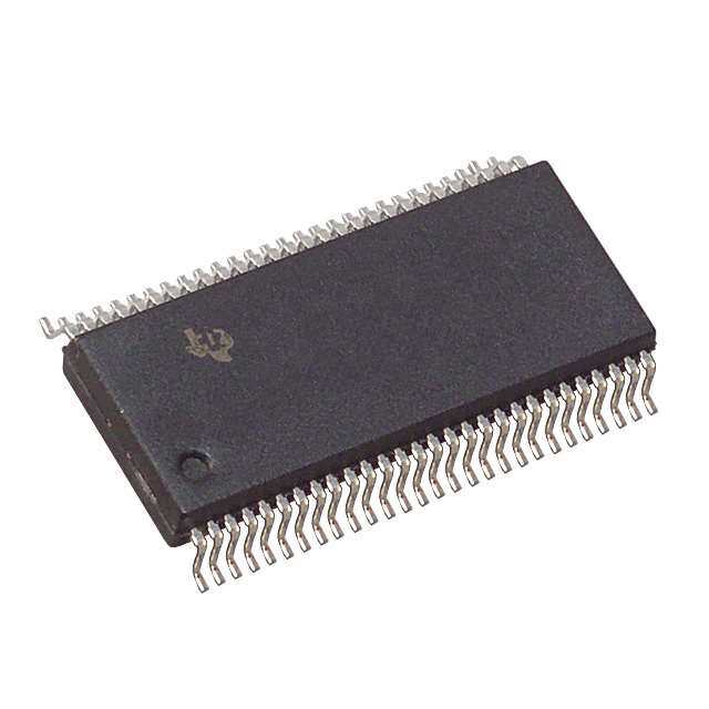
| 描述 | IC OCT D-TYPE LATCH 20-DIP闭锁 Octal Trans D-Type 闭锁 |
| 产品分类 | |
| 品牌 | Texas Instruments |
| 产品手册 | |
| 产品图片 |
|
| rohs | 符合RoHS无铅 / 符合限制有害物质指令(RoHS)规范要求 |
| 产品系列 | 逻辑集成电路,闭锁,Texas Instruments SN74F573N74F |
| 数据手册 | |
| 产品型号 | SN74F573N |
| PCN设计/规格 | |
| 产品目录页面 | |
| 产品种类 | 闭锁 |
| 传播延迟时间 | 7 ns at 5 V |
| 低电平输出电流 | 32 mA |
| 供应商器件封装 | 20-PDIP |
| 其它名称 | 296-3599-5 |
| 包装 | 管件 |
| 单位重量 | 1.199 g |
| 商标 | Texas Instruments |
| 安装类型 | 通孔 |
| 安装风格 | Through Hole |
| 封装 | Tube |
| 封装/外壳 | 20-DIP(0.300",7.62mm) |
| 封装/箱体 | PDIP-20 |
| 工作温度 | 0°C ~ 70°C |
| 工厂包装数量 | 20 |
| 延迟时间-传播 | 8.6ns |
| 最大工作温度 | + 70 C |
| 最小工作温度 | 0 C |
| 极性 | Non-Inverting |
| 标准包装 | 20 |
| 独立电路 | 1 |
| 电压-电源 | 4.5 V ~ 5.5 V |
| 电流-输出高,低 | 3mA,24mA |
| 电源电压-最大 | 5.5 V |
| 电源电压-最小 | 4.5 V |
| 电路 | 8:8 |
| 电路数量 | 8 Circuit |
| 系列 | SN74F573 |
| 输入线路数量 | 8 Line |
| 输出类型 | 三态 |
| 输出线路数量 | 8 Line |
| 逻辑类型 | D 型透明锁存器 |
| 逻辑系列 | F |
| 高电平输出电流 | - 3 mA |


- 商务部:美国ITC正式对集成电路等产品启动337调查
- 曝三星4nm工艺存在良率问题 高通将骁龙8 Gen1或转产台积电
- 太阳诱电将投资9.5亿元在常州建新厂生产MLCC 预计2023年完工
- 英特尔发布欧洲新工厂建设计划 深化IDM 2.0 战略
- 台积电先进制程称霸业界 有大客户加持明年业绩稳了
- 达到5530亿美元!SIA预计今年全球半导体销售额将创下新高
- 英特尔拟将自动驾驶子公司Mobileye上市 估值或超500亿美元
- 三星加码芯片和SET,合并消费电子和移动部门,撤换高东真等 CEO
- 三星电子宣布重大人事变动 还合并消费电子和移动部门
- 海关总署:前11个月进口集成电路产品价值2.52万亿元 增长14.8%


PDF Datasheet 数据手册内容提取
(cid:1)(cid:2)(cid:3)(cid:4)(cid:5)(cid:3)(cid:6)(cid:7)(cid:8)(cid:9)(cid:1)(cid:2)(cid:6)(cid:4)(cid:5)(cid:3)(cid:6)(cid:7) (cid:10)(cid:11)(cid:12)(cid:13)(cid:14)(cid:9)(cid:12)(cid:15)(cid:13)(cid:2)(cid:1)(cid:16)(cid:13)(cid:15)(cid:17)(cid:2)(cid:12)(cid:9)(cid:18)(cid:19)(cid:12)(cid:20)(cid:16)(cid:17)(cid:9)(cid:14)(cid:13)(cid:12)(cid:11)(cid:21)(cid:17)(cid:1) (cid:22)(cid:23)(cid:12)(cid:21)(cid:9)(cid:7)(cid:19)(cid:1)(cid:12)(cid:13)(cid:12)(cid:17)(cid:9)(cid:10)(cid:24)(cid:12)(cid:16)(cid:24)(cid:12)(cid:1) SDFS011A − MARCH 1987 − REVISED OCTOBER 1993 • Eight Latches in a Single Package SN54F573...J PACKAGE • SN74F573...DW OR N PACKAGE 3-State Bus-Driving True Outputs (TOP VIEW) • Full Parallel Access for Loading • Buffered Control Inputs OE 1 20 VCC • Package Options Include Plastic 1D 2 19 1Q Small-Outline Packages, Ceramic Chip 2D 3 18 2Q Carriers, and Standard Plastic and Ceramic 3D 4 17 3Q 300-mil DIPs 4D 5 16 4Q 5D 6 15 5Q description 6D 7 14 6Q 7D 8 13 7Q These 8-bit latches feature 3-state outputs 8D 9 12 8Q designed specifically for driving highly capacitive GND 10 11 LE or relatively low-impedance loads. They are particularly suitable for implementing buffer registers, I/O ports, bidirectional bus drivers, and SN54F573...FK PACKAGE (TOP VIEW) working registers. C The eight latches of the ′F573 are transparent 2D 1D OEVC1Q D-type latches. While the latch enable (LE) input is high, the Q outputs follow the data (D) inputs. 3 2 1 20 19 3D 4 18 2Q When the latch enable is taken low, the Q outputs 4D 5 17 3Q are latched at the logic levels set up at the D 5D 6 16 4Q inputs. 6D 7 15 5Q A buffered output enable (OE) input can be used 7D 8 14 6Q 9 10 11 12 13 to place the eight outputs in either a normal logic state (high or low logic levels) or a high- D D EQ Q 8 N L8 7 impedance state. In the high-impedance state, the G outputs neither load nor drive the bus lines significantly. The high-impedance state and increased drive provide the capability to drive bus lines without need for interface or pullup components. The output enable (OE) input does not affect the internal operations of the latches. Old data can be retained or new data can be entered while the outputs are in the high-impedance state. The SN54F573 is characterized for operation over the full military temperature range of −55°C to 125°C. The SN74F573 is characterized for operation from 0°C to 70°C. FUNCTION TABLE (each latch) INPUTS OOUUTTPPUUTT OE LE D Q L H H H L H L L L L X Q0 H X X Z (cid:16)(cid:15)(cid:10)(cid:18)(cid:24)(cid:11)(cid:12)(cid:23)(cid:10)(cid:2) (cid:18)(cid:13)(cid:12)(cid:13) (cid:25)(cid:26)(cid:27)(cid:28)(cid:29)(cid:30)(cid:31)!(cid:25)(cid:28)(cid:26) (cid:25)" #$(cid:29)(cid:29)%(cid:26)! (cid:31)" (cid:28)(cid:27) &$’((cid:25)#(cid:31)!(cid:25)(cid:28)(cid:26) )(cid:31)!%* Copyright 1993, Texas Instruments Incorporated (cid:16)(cid:29)(cid:28))$#!" #(cid:28)(cid:26)(cid:27)(cid:28)(cid:29)(cid:30) !(cid:28) "&%#(cid:25)(cid:27)(cid:25)#(cid:31)!(cid:25)(cid:28)(cid:26)" &%(cid:29) !+% !%(cid:29)(cid:30)" (cid:28)(cid:27) (cid:12)%,(cid:31)" (cid:23)(cid:26)"!(cid:29)$(cid:30)%(cid:26)!" "!(cid:31)(cid:26))(cid:31)(cid:29)) -(cid:31)(cid:29)(cid:29)(cid:31)(cid:26)!.* (cid:16)(cid:29)(cid:28))$#!(cid:25)(cid:28)(cid:26) &(cid:29)(cid:28)#%""(cid:25)(cid:26)/ )(cid:28)%" (cid:26)(cid:28)! (cid:26)%#%""(cid:31)(cid:29)(cid:25)(. (cid:25)(cid:26)#($)% !%"!(cid:25)(cid:26)/ (cid:28)(cid:27) (cid:31)(( &(cid:31)(cid:29)(cid:31)(cid:30)%!%(cid:29)"* POST OFFICE BOX 655303 • DALLAS, TEXAS 75265 2−1 • POST OFFICE BOX 1443 HOUSTON, TEXAS 77251−1443
(cid:1)(cid:2)(cid:3)(cid:4)(cid:5)(cid:3)(cid:6)(cid:7)(cid:8)(cid:9)(cid:1)(cid:2)(cid:6)(cid:4)(cid:5)(cid:3)(cid:6)(cid:7) (cid:10)(cid:11)(cid:12)(cid:13)(cid:14)(cid:9)(cid:12)(cid:15)(cid:13)(cid:2)(cid:1)(cid:16)(cid:13)(cid:15)(cid:17)(cid:2)(cid:12)(cid:9)(cid:18)(cid:19)(cid:12)(cid:20)(cid:16)(cid:17)(cid:9)(cid:14)(cid:13)(cid:12)(cid:11)(cid:21)(cid:17)(cid:1) (cid:22)(cid:23)(cid:12)(cid:21)(cid:9)(cid:7)(cid:19)(cid:1)(cid:12)(cid:13)(cid:12)(cid:17)(cid:9)(cid:10)(cid:24)(cid:12)(cid:16)(cid:24)(cid:12)(cid:1) SDFS011A − MARCH 1987 − REVISED OCTOBER 1993 logic symbol† logic diagram (positive logic) 1 1 OE EN OE 11 LE C1 11 LE 2 19 1D 1D 1Q 3 18 C1 2D 2Q 19 4 17 2 1Q 3D 3Q 1D 1D 5 16 4D 4Q 6 15 5D 5Q 7 14 6D 6Q 8 13 7D 7Q 9 12 To Seven Other Channels 8D 8Q †This symbol is in accordance with ANSI/IEEE Std 91-1984 and IEC Publication 617-12. absolute maximum ratings over operating free-air temperature range (unless otherwise noted)‡ Supply voltage range, V . . . . . . . . . . . . . . . . . . . . . . . . . . . . . . . . . . . . . . . . . . . . . . . . . . . . . . . . . . −0.5 V to 7 V CC Input voltage range, V (see Note 1) . . . . . . . . . . . . . . . . . . . . . . . . . . . . . . . . . . . . . . . . . . . . . . . . . . −1.2 V to 7 V I Input current range . . . . . . . . . . . . . . . . . . . . . . . . . . . . . . . . . . . . . . . . . . . . . . . . . . . . . . . . . . . . . . −30 mA to 5 mA Voltage range applied to any output in the disabled or power-off state . . . . . . . . . . . . . . . . . . . −0.5 V to 5.5 V Voltage range applied to any output in the high state . . . . . . . . . . . . . . . . . . . . . . . . . . . . . . . . . . −0.5 V to V CC Current into any output in the low state:SN54F573 . . . . . . . . . . . . . . . . . . . . . . . . . . . . . . . . . . . . . . . . . . . 40 mA SN74F573 . . . . . . . . . . . . . . . . . . . . . . . . . . . . . . . . . . . . . . . . . . . 48 mA Operating free-air temperature range: SN54F573 . . . . . . . . . . . . . . . . . . . . . . . . . . . . . . . . . . . −55°C to 125°C SN74F573 . . . . . . . . . . . . . . . . . . . . . . . . . . . . . . . . . . . . . . 0°C to 70°C Storage temperature range . . . . . . . . . . . . . . . . . . . . . . . . . . . . . . . . . . . . . . . . . . . . . . . . . . . . . . . . −65°C to 150°C ‡Stresses beyond those listed under “absolute maximum ratings” may cause permanent damage to the device. These are stress ratings only and functional operation of the device at these or any other conditions beyond those indicated under “recommended operating conditions” is not implied. Exposure to absolute-maximum-rated conditions for extended periods may affect device reliability. NOTE 1: The input voltage ratings may be exceeded provided the input current ratings are observed. recommended operating conditions SN54F573 SN74F573 UUNNIITT MIN NOM MAX MIN NOM MAX VCC Supply voltage 4.5 5 5.5 4.5 5 5.5 V VIH High-level input voltage 2 2 V VIL Low-level input voltage 0.8 0.8 V IIK Input clamp current −18 −18 mA IOH High-level output current −3 −3 mA IOL Low-level output current 20 24 mA TA Operating free-air temperature −55 125 0 70 °C 2−2 POST OFFICE BOX 65•5303 • DALLAS, TEXAS 75265 POST OFFICE BOX 1443 HOUSTON, TEXAS 77251−1443
(cid:1)(cid:2)(cid:3)(cid:4)(cid:5)(cid:3)(cid:6)(cid:7)(cid:8)(cid:9)(cid:1)(cid:2)(cid:6)(cid:4)(cid:5)(cid:3)(cid:6)(cid:7) (cid:10)(cid:11)(cid:12)(cid:13)(cid:14)(cid:9)(cid:12)(cid:15)(cid:13)(cid:2)(cid:1)(cid:16)(cid:13)(cid:15)(cid:17)(cid:2)(cid:12)(cid:9)(cid:18)(cid:19)(cid:12)(cid:20)(cid:16)(cid:17)(cid:9)(cid:14)(cid:13)(cid:12)(cid:11)(cid:21)(cid:17)(cid:1) (cid:22)(cid:23)(cid:12)(cid:21)(cid:9)(cid:7)(cid:19)(cid:1)(cid:12)(cid:13)(cid:12)(cid:17)(cid:9)(cid:10)(cid:24)(cid:12)(cid:16)(cid:24)(cid:12)(cid:1) SDFS011A − MARCH 1987 − REVISED OCTOBER 1993 electrical characteristics over recommended operating free-air temperature range (unless otherwise noted) SN54F573 SN74F573 PPAARRAAMMEETTEERR TTEESSTT CCOONNDDIITTIIOONNSS UUNNIITT MIN TYP† MAX MIN TYP† MAX VIK VCC = 4.5 V, II = −18 mA −1.2 −1.2 V IOH = −1 mA 2.5 3.4 2.5 3.4 VVCCCC == 44..55 VV VOH IOH = −3 mA 2.4 3.3 2.4 3.3 V VCC = 4.75 V, IOH = −1 mA to −3 mA 2.7 IOL = 20 mA 0.3 0.5 VVOOLL VVCCCC == 44..55 VV VV IOL = 24 mA 0.35 0.5 IOZH VCC = 5.5 V, VO = 2.7 V 50 50 µA IOZL VCC = 5.5 V, VO = 0.5 V −50 −50 µA II VCC = 5.5 V, VI = 7 V 0.1 0.1 mA IIH VCC = 5.5 V, VI = 2.7 V 20 20 µA IIL VCC = 5.5 V, VI = 0.5 V −0.6 −0.6 mA IOS‡ VCC = 5.5 V, VO = 0 −60 −150 −60 −150 mA ICCZ VCC = 5.5 V, See Note 2 38 55 38 55 mA †All typical values are at VCC = 5 V, TA = 25°C. ‡Not more than one output should be shorted at a time, and the duration of the short circuit should not exceed one second. NOTE 2: ICCZ is measured with OE at 4.5 V and all other inputs grounded. timing requirements over recommended ranges of supply voltage and operating free-air temperature (unless otherwise noted) VCC = 5 V, TA = 25°C SSNN5544FF557733 SSNN7744FF557733 UUNNIITT ′F573 MIN MAX MIN MAX MIN MAX tw Pulse duration, LE high 6 6 6 ns tsu Setup time, data before LE↓ 2 2 2 ns th Hold time, data after LE↓ 3 3 3 ns switching characteristics (see Note 3) VCC = 5 V, VCC = 4.5 V to 5.5 V, CL = 50 pF, CL = 50 pF, FROM TO RL = 500 Ω, RL = 500Ω, PARAMETER ((IINNPPUUTT)) ((OOUUTTPPUUTT)) TA = 25°C TA = MIN to MAX§ UNIT ′F573 SN54F573 SN74F573 MIN TYP MAX MIN MAX MIN MAX tPLH 2 4.9 7 1.5 9 2.2 8 DD QQ nnss tPHL 1.2 3.3 5 1 8 1.2 6 tPLH 4.2 8.6 11.5 3.7 13.5 4.2 13 LLEE QQ nnss tPHL 2.2 4.8 7 1.5 9 2.2 8 tPZH 1.2 4.6 11 1 13 1.2 12 OOEE QQ nnss tPZL 1.2 5.2 7.5 1 10 1.2 8.5 tPHZ 1.2 4.1 6.5 1 8.5 1.2 7.5 OOEE QQ nnss tPLZ 1.2 3.4 6 1 7 1.2 6 §For conditions shown as MIN or MAX, use the appropriate value specified under recommended operating conditions. NOTE 3: Load circuits and waveforms are shown in Section 1. POST OFFICE BOX 65•5303 • DALLAS, TEXAS 75265 2−3 POST OFFICE BOX 1443 HOUSTON, TEXAS 77251−1443
(cid:1)(cid:2)(cid:3)(cid:4)(cid:5)(cid:3)(cid:6)(cid:7)(cid:8)(cid:9)(cid:1)(cid:2)(cid:6)(cid:4)(cid:5)(cid:3)(cid:6)(cid:7) (cid:10)(cid:11)(cid:12)(cid:13)(cid:14)(cid:9)(cid:12)(cid:15)(cid:13)(cid:2)(cid:1)(cid:16)(cid:13)(cid:15)(cid:17)(cid:2)(cid:12)(cid:9)(cid:18)(cid:19)(cid:12)(cid:20)(cid:16)(cid:17)(cid:9)(cid:14)(cid:13)(cid:12)(cid:11)(cid:21)(cid:17)(cid:1) (cid:22)(cid:23)(cid:12)(cid:21)(cid:9)(cid:7)(cid:19)(cid:1)(cid:12)(cid:13)(cid:12)(cid:17)(cid:9)(cid:10)(cid:24)(cid:12)(cid:16)(cid:24)(cid:12)(cid:1) SDFS011A − MARCH 1987 − REVISED OCTOBER 1993 2−4 POST OFFICE BOX 65•5303 • DALLAS, TEXAS 75265 POST OFFICE BOX 1443 HOUSTON, TEXAS 77251−1443
IMPORTANTNOTICE TexasInstrumentsIncorporatedanditssubsidiaries(TI)reservetherighttomakecorrections,modifications,enhancements,improvements, andotherchangestoitsproductsandservicesatanytimeandtodiscontinueanyproductorservicewithoutnotice.Customersshould obtainthelatestrelevantinformationbeforeplacingordersandshouldverifythatsuchinformationiscurrentandcomplete.Allproductsare soldsubjecttoTI’stermsandconditionsofsalesuppliedatthetimeoforderacknowledgment. TIwarrantsperformanceofitshardwareproductstothespecificationsapplicableatthetimeofsaleinaccordancewithTI’sstandard warranty.TestingandotherqualitycontroltechniquesareusedtotheextentTIdeemsnecessarytosupportthiswarranty.Exceptwhere mandatedbygovernmentrequirements,testingofallparametersofeachproductisnotnecessarilyperformed. TIassumesnoliabilityforapplicationsassistanceorcustomerproductdesign.Customersareresponsiblefortheirproductsand applicationsusingTIcomponents.Tominimizetherisksassociatedwithcustomerproductsandapplications,customersshouldprovide adequatedesignandoperatingsafeguards. TIdoesnotwarrantorrepresentthatanylicense,eitherexpressorimplied,isgrantedunderanyTIpatentright,copyright,maskworkright, orotherTIintellectualpropertyrightrelatingtoanycombination,machine,orprocessinwhichTIproductsorservicesareused.Information publishedbyTIregardingthird-partyproductsorservicesdoesnotconstitutealicensefromTItousesuchproductsorservicesora warrantyorendorsementthereof.Useofsuchinformationmayrequirealicensefromathirdpartyunderthepatentsorotherintellectual propertyofthethirdparty,oralicensefromTIunderthepatentsorotherintellectualpropertyofTI. ReproductionofTIinformationinTIdatabooksordatasheetsispermissibleonlyifreproductioniswithoutalterationandisaccompanied byallassociatedwarranties,conditions,limitations,andnotices.Reproductionofthisinformationwithalterationisanunfairanddeceptive businesspractice.TIisnotresponsibleorliableforsuchaltereddocumentation.Informationofthirdpartiesmaybesubjecttoadditional restrictions. ResaleofTIproductsorserviceswithstatementsdifferentfromorbeyondtheparametersstatedbyTIforthatproductorservicevoidsall expressandanyimpliedwarrantiesfortheassociatedTIproductorserviceandisanunfairanddeceptivebusinesspractice.TIisnot responsibleorliableforanysuchstatements. TIproductsarenotauthorizedforuseinsafety-criticalapplications(suchaslifesupport)whereafailureoftheTIproductwouldreasonably beexpectedtocauseseverepersonalinjuryordeath,unlessofficersofthepartieshaveexecutedanagreementspecificallygoverning suchuse.Buyersrepresentthattheyhaveallnecessaryexpertiseinthesafetyandregulatoryramificationsoftheirapplications,and acknowledgeandagreethattheyaresolelyresponsibleforalllegal,regulatoryandsafety-relatedrequirementsconcerningtheirproducts andanyuseofTIproductsinsuchsafety-criticalapplications,notwithstandinganyapplications-relatedinformationorsupportthatmaybe providedbyTI.Further,BuyersmustfullyindemnifyTIanditsrepresentativesagainstanydamagesarisingoutoftheuseofTIproductsin suchsafety-criticalapplications. TIproductsareneitherdesignednorintendedforuseinmilitary/aerospaceapplicationsorenvironmentsunlesstheTIproductsare specificallydesignatedbyTIasmilitary-gradeor"enhancedplastic."OnlyproductsdesignatedbyTIasmilitary-grademeetmilitary specifications.BuyersacknowledgeandagreethatanysuchuseofTIproductswhichTIhasnotdesignatedasmilitary-gradeissolelyat theBuyer'srisk,andthattheyaresolelyresponsibleforcompliancewithalllegalandregulatoryrequirementsinconnectionwithsuchuse. TIproductsareneitherdesignednorintendedforuseinautomotiveapplicationsorenvironmentsunlessthespecificTIproductsare designatedbyTIascompliantwithISO/TS16949requirements.Buyersacknowledgeandagreethat,iftheyuseanynon-designated productsinautomotiveapplications,TIwillnotberesponsibleforanyfailuretomeetsuchrequirements. FollowingareURLswhereyoucanobtaininformationonotherTexasInstrumentsproductsandapplicationsolutions: Products Applications Amplifiers amplifier.ti.com Audio www.ti.com/audio DataConverters dataconverter.ti.com Automotive www.ti.com/automotive DSP dsp.ti.com Broadband www.ti.com/broadband ClocksandTimers www.ti.com/clocks DigitalControl www.ti.com/digitalcontrol Interface interface.ti.com Medical www.ti.com/medical Logic logic.ti.com Military www.ti.com/military PowerMgmt power.ti.com OpticalNetworking www.ti.com/opticalnetwork Microcontrollers microcontroller.ti.com Security www.ti.com/security RFID www.ti-rfid.com Telephony www.ti.com/telephony RF/IFandZigBee®Solutions www.ti.com/lprf Video&Imaging www.ti.com/video Wireless www.ti.com/wireless MailingAddress:TexasInstruments,PostOfficeBox655303,Dallas,Texas75265 Copyright©2008,TexasInstrumentsIncorporated