ICGOO在线商城 > 集成电路(IC) > 逻辑 - 信号开关,多路复用器,解码器 > SN74CB3Q3306APWR
 Datasheet下载
- 型号: SN74CB3Q3306APWR
- 制造商: Texas Instruments
- 库位|库存: xxxx|xxxx
- 要求:
| 数量阶梯 | 香港交货 | 国内含税 |
| +xxxx | $xxxx | ¥xxxx |
查看当月历史价格
查看今年历史价格
SN74CB3Q3306APWR产品简介:
ICGOO电子元器件商城为您提供SN74CB3Q3306APWR由Texas Instruments设计生产,在icgoo商城现货销售,并且可以通过原厂、代理商等渠道进行代购。 SN74CB3Q3306APWR价格参考。Texas InstrumentsSN74CB3Q3306APWR封装/规格:逻辑 - 信号开关,多路复用器,解码器, Bus Switch 1 x 1:1 8-TSSOP。您可以下载SN74CB3Q3306APWR参考资料、Datasheet数据手册功能说明书,资料中有SN74CB3Q3306APWR 详细功能的应用电路图电压和使用方法及教程。
Texas Instruments 的 SN74CB3Q3306APWR 是一款高性能、低电压的信号开关/多路复用器芯片,广泛应用于需要高速数据切换和路由的场景。其主要应用场景包括:

1. 通信系统:用于在不同数据通道之间快速切换,适用于路由器、交换机等网络设备中的信号路径管理。

2. 测试与测量设备:作为多路复用器使用时,可以实现对多个输入信号的轮流采集与分析,提高测试效率。

3. 工业控制:在PLC(可编程逻辑控制器)或自动化系统中,用于选择不同的传感器或执行器信号路径。

4. 消费类电子产品:如音视频切换器、便携式设备中的信号源选择等场景。

5. 计算机外设:用于USB或其他接口之间的信号切换,支持热插拔功能,确保信号传输的稳定性。

该器件具有低导通电阻、宽电源电压范围(1.65V 至 3.6V),支持双向信号传输,并且兼容多种数字电平,适合低功耗与高性能并重的应用场合。
| 参数 | 数值 |
| 产品目录 | 集成电路 (IC)半导体 |
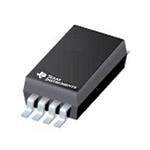
| 描述 | IC DUAL FET BUS SWITCH 8-TSSOP数字总线开关 IC Lo-Vltg Hi-Bandwidth Bus Switch |
| 产品分类 | |
| 品牌 | Texas Instruments |
| 产品手册 | |
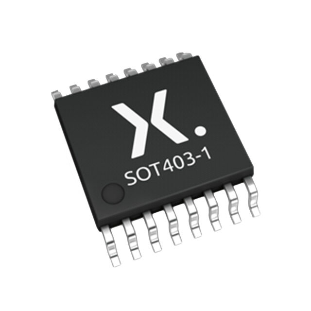
| 产品图片 |
|
| rohs | 符合RoHS无铅 / 符合限制有害物质指令(RoHS)规范要求 |
| 产品系列 | 开关 IC,数字总线开关 IC,Texas Instruments SN74CB3Q3306APWR74CB |
| 数据手册 | |
| 产品型号 | SN74CB3Q3306APWR |
| 产品目录页面 | |
| 产品种类 | 数字总线开关 IC |
| 传播延迟时间 | 0.2 ns |
| 供应商器件封装 | 8-TSSOP |
| 其它名称 | 296-15102-1 |
| 包装 | 剪切带 (CT) |
| 单位重量 | 39 mg |
| 商标 | Texas Instruments |
| 安装类型 | 表面贴装 |
| 安装风格 | SMD/SMT |
| 导通电阻—最大值 | 9 Ohms |
| 封装 | Reel |
| 封装/外壳 | 8-TSSOP(0.173",4.40mm 宽) |
| 封装/箱体 | TSSOP-8 |
| 工作温度 | -40°C ~ 85°C |
| 工厂包装数量 | 2000 |
| 开关数量 | 2 |
| 技术 | CB3Q |
| 最大工作温度 | + 85 C |
| 最小工作温度 | - 40 C |
| 标准包装 | 1 |
| 独立电路 | 2 |
| 电压-电源 | 2.3 V ~ 3.6 V |
| 电压源 | 单电源 |
| 电流-输出高,低 | - |
| 电源电压-最大 | 3.6 V |
| 电源电压-最小 | 2.3 V |
| 电源电流 | 250 uA |
| 电路 | 1 x 1:1 |
| 类型 | FET 总线开关 |
| 系列 | SN74CB3Q3306A |
| 逻辑系列 | CB3Q |


PDF Datasheet 数据手册内容提取
SN74CB3Q3306A www.ti.com SCDS113E–DECEMBER2002–REVISEDJANUARY2011 Dual FET Bus Switch 2.5-V/3.3-V Low-Voltage High-Bandwidth Bus Switch CheckforSamples:SN74CB3Q3306A FEATURES • DataandControlInputsProvideUndershoot 1 • High-BandwidthDataPath(upto500MHz(1)) ClampDiodes • 5-V-TolerantI/OsWithDevicePoweredUpor • LowPowerConsumption(ICC=0.25mATyp) PoweredDown • V OperatingRangeFrom2.3Vto3.6V CC • LowandFlatON-StateResistance(r ) • DataI/OsSupport0-to5-VSignalingLevels on CharacteristicsOverOperatingRange (0.8V,1.2V,1.5V,1.8V,2.5V,3.3V,5V) (ron=4ΩTyp) • ControlInputsCanBeDrivenbyTTLor • Rail-to-RailSwitchingonDataI/OPorts 5-V/3.3-VCMOSOutputs – 0-to5-VSwitchingWith3.3-VV • I SupportsPartial-Power-DownMode CC off – 0-to3.3-VSwitchingWith2.5-VV Operation CC • BidirectionalDataFlowWithNear-Zero • Latch-UpPerformanceExceeds100mA PropagationDelay PerJESD78,ClassII • LowInput/OutputCapacitanceMinimizes • ESDPerformanceTestedPerJESD22 LoadingandSignalDistortion – 2000-VHuman-BodyModel (C =3.5pFTyp) (A114-B,ClassII) io(OFF) • FastSwitchingFrequency(f =20MHzMax) – 1000-VCharged-DeviceModel(C101) OE (1) Foradditionalinformationregardingtheperformance • SupportsBothDigitalandAnalog characteristicsoftheCB3Qfamily,refertotheTIapplication Applications:USBInterface,DifferentialSignal report,CBT-C,CB3T,andCB3QSignal-SwitchFamilies, Interface,BusIsolation,Low-DistortionSignal literaturenumberSCDA008. Gating DCU PACKAGE PW PACKAGE (TOP VIEW) (TOP VIEW) 1OE 1 8 VCC 1OE 1 8 VCC 1A 2 7 2OE 1A 2 7 2OE 1B 3 6 2B 1B 3 6 2B GND 4 5 2A GND 4 5 2A ORDERINGINFORMATION T PACKAGE(1) ORDERABLEPARTNUMBER TOP-SIDEMARKING A Tube SN74CB3Q3306APW TSSOP–PW BU306A Tapeandreel SN74CB3Q3306APWR –40°Cto85°C SN74CB3Q3306ADCUR US8-DCU Tapeandreel GA6R(2) 74CB3Q3306ADCURE4 (1) Packagedrawings,standardpackingquantities,thermaldata,symbolization,andPCBdesignguidelinesareavailableat www.ti.com/sc/package. (2) Thelastcharacterdesignatesassembly/testsite. 1 Pleasebeawarethatanimportantnoticeconcerningavailability,standardwarranty,anduseincriticalapplicationsofTexas Instrumentssemiconductorproductsanddisclaimerstheretoappearsattheendofthisdatasheet. PRODUCTIONDATAinformationiscurrentasofpublicationdate. Copyright©2002–2011,TexasInstrumentsIncorporated Products conform to specifications per the terms of the Texas Instruments standard warranty. Production processing does not necessarilyincludetestingofallparameters.
SN74CB3Q3306A SCDS113E–DECEMBER2002–REVISEDJANUARY2011 www.ti.com Thesedeviceshavelimitedbuilt-inESDprotection.Theleadsshouldbeshortedtogetherorthedeviceplacedinconductivefoam duringstorageorhandlingtopreventelectrostaticdamagetotheMOSgates. DESCRIPTION/ORDERING INFORMATION The SN74CB3Q3306A is a high-bandwidth FET bus switch utilizing a charge pump to elevate the gate voltage of thepasstransistor,providingalowandflatON-stateresistance(r ).ThelowandflatON-stateresistanceallows on for minimal propagation delay and supports rail-to-rail switching on the data input/output (I/O) ports. The device also features low data I/O capacitance to minimize capacitive loading and signal distortion on the data bus. Specifically designed to support high-bandwidth applications, the SN74CB3Q3306A provides an optimized interface solution ideally suited for broadband communications, networking, and data-intensive computing systems. The SN74CB3Q3306A is organized as two 1-bit switches with separate output-enable (1OE, 2OE) inputs. It can be used as two 1-bit bus switches or as one 2-bit bus switch. When OE is low, the associated 1-bit bus switch is ON and the A port is connected to the B port, allowing bidirectional data flow between ports. When OE is high, theassociated1-bitbusswitchisOFF,andahigh-impedancestateexistsbetweentheAandBports. This device is fully specified for partial-power-down applications using I . The I circuitry prevents damaging off off currentbackflowthroughthedevicewhenitispowereddown.Thedevicehasisolationduringpoweroff. To ensure the high-impedance state during power up or power down, OE should be tied to V through a pullup CC resistor;theminimumvalueoftheresistorisdeterminedbythecurrent-sinkingcapabilityofthedriver. Table1.FUNCTIONTABLE (EACHBUSSWITCH) INPUT INPUT/OUTPUT FUNCTION OE A L B Aport=Bport H Z Disconnect LOGICDIAGRAM(POSITIVELOGIC) 2 3 1A SW 1B 1 1OE 5 6 2A SW 2B 7 2OE 2 SubmitDocumentationFeedback Copyright©2002–2011,TexasInstrumentsIncorporated ProductFolderLink(s):SN74CB3Q3306A
SN74CB3Q3306A www.ti.com SCDS113E–DECEMBER2002–REVISEDJANUARY2011 SIMPLIFIEDSCHEMATIC,EACHFETSWITCH(SW) A B VCC Charge Pump EN(1) (1) EN is the internal enable signal applied to the switch. ABSOLUTE MAXIMUM RATINGS(1) overoperatingfree-airtemperaturerange(unlessotherwisenoted) MIN MAX UNIT V Supplyvoltagerange –0.5 4.6 V CC V Controlinputvoltagerange(2)(3) –0.5 7 V IN V SwitchI/Ovoltagerange(2) (3) (4) –0.5 7 V I/O I Controlinputclampcurrent V <0 –50 mA IK IN I I/Oportclampcurrent V <0 –50 mA I/OK I/O I ON-stateswitchcurrent(5) ±64 mA I/O ContinuouscurrentthrougheachV or ±100 mA CC GND DCU TBD q Packagethermalimpedance(6) °C/W JA PW 88 T Storagetemperaturerange –65 150 °C stg (1) Stressesbeyondthoselistedunder"absolutemaximumratings"maycausepermanentdamagetothedevice.Thesearestressratings only,andfunctionaloperationofthedeviceattheseoranyotherconditionsbeyondthoseindicatedunder"recommendedoperating conditions"isnotimplied.Exposuretoabsolute-maximum-ratedconditionsforextendedperiodsmayaffectdevicereliability. (2) Allvoltagesarewithrespecttoground,unlessotherwisespecified. (3) Theinputandoutputvoltageratingsmaybeexceedediftheinputandoutputclamp-currentratingsareobserved. (4) V andV areusedtodenotespecificconditionsforV . I O I/O (5) I andI areusedtodenotespecificconditionsforI . I O I/O (6) ThepackagethermalimpedanceiscalculatedinaccordancewithJESD51-7. RECOMMENDED OPERATING CONDITIONS(1) MIN MAX UNIT V Supplyvoltage 2.3 3.6 V CC High-levelcontrolinput VCC=2.3Vto2.7V 1.7 5.5 V V IH voltage V =2.7Vto3.6V 2 5.5 CC Low-levelcontrolinput VCC=2.3Vto2.7V 0 0.7 V V IL voltage V =2.7Vto3.6V 0 0.8 CC V Datainput/outputvoltage 0 5.5 V I/O T Operatingfree-airtemperature –40 85 °C A (1) AllunusedcontrolinputsofthedevicemustbeheldatV orGNDtoensureproperdeviceoperation.RefertotheTIapplicationreport, CC ImplicationsofSloworFloatingCMOSInputs,literaturenumberSCBA004. Copyright©2002–2011,TexasInstrumentsIncorporated SubmitDocumentationFeedback 3 ProductFolderLink(s):SN74CB3Q3306A
SN74CB3Q3306A SCDS113E–DECEMBER2002–REVISEDJANUARY2011 www.ti.com ELECTRICAL CHARACTERISTICS(1) overrecommendedoperatingfree-airtemperaturerange(unlessotherwisenoted) PARAMETER TESTCONDITIONS MIN TYP(2) MAX UNIT V V =3.6V, I =–18mA –1.8 V IK CC I I Controlinputs V =3.6V, V =0to5.5V ±1 mA IN CC IN I (3) V =3.6V, VO=0to5.5V, SwitchOFF, ±1 mA OZ CC V =0, V =V orGND I IN CC I V =0, V =0to5.5V, V =0 1 mA off CC O I I =0, I V =3.6V, I/O V =V orGND 0.25 0.7 mA CC CC SwitchONorOFF, IN CC ΔI (4) Controlinputs V =3.6V, Oneinputat3V, OtherinputsatV orGND 25 mA CC CC CC I (5) Percontrol VCC=3.6V, AandBportsopen, 0.03 0.1 mA/ CCD input Controlinputswitchingat50%dutycycle MHz C Controlinputs V =3.3V, V =5.5V,3.3V,or0 2.5 3.5 pF in CC IN SwitchOFF, C V =3.3V, V =5.5V,3.3V,or0 3.5 5 pF io(OFF) CC V =V orGND, I/O IN CC SwitchON, C V =3.3V, V =5.5V,3.3V,or0 8 10.5 pF io(ON) CC V =V orGND, I/O IN CC VCC=2.3V, VI=0, IO=30mA 4 8 r (6) TYPatVCC=2.5V VI=1.7V, IO=–15mA 5 9 Ω on V =0, I =30mA 4 6 I O V =3V CC V =2.4V, I =–15mA 5 8 I O (1) V andI refertocontrolinputs.V,V ,I,andI refertodatapins. IN IN I O I O (2) AlltypicalvaluesareatV =3.3V(unlessotherwisenoted),T =25°C. CC A (3) ForI/Oports,theparameterI includestheinputleakagecurrent. OZ (4) ThisistheincreaseinsupplycurrentforeachinputthatisatthespecifiedTTLvoltagelevel,ratherthanV orGND. CC (5) Thisparameterspecifiesthedynamicpower-supplycurrentassociatedwiththeoperatingfrequencyofasinglecontrolinput(see Figure2). (6) MeasuredbythevoltagedropbetweentheAandBterminalsattheindicatedcurrentthroughtheswitch.ON-stateresistanceis determinedbythelowerofthevoltagesofthetwo(AorB)terminals. SWITCHING CHARACTERISTICS overrecommendedoperatingfree-airtemperaturerange(unlessotherwisenoted)(seeFigure3) V =2.5V V =3.3V CC CC PARAMETER FROM TO ±0.2V ±0.3V UNIT (INPUT) (OUTPUT) MIN MAX MIN MAX f (1) OE AorB 10 20 MHz OE t (2) AorB BorA 0.2 0.2 ns pd t OE AorB 1.5 6.5 1.5 5.5 ns en t OE AorB 1 6 1 5 ns dis (1) Maximumswitchingfrequencyforcontrolinput(V >V ,V =5V,R ≥1MΩ,C =0) O CC I L L (2) ThepropagationdelayisthecalculatedRCtimeconstantofthetypicalON-stateresistanceoftheswitchandthespecifiedload capacitance,whendrivenbyanidealvoltagesource(zerooutputimpedance). 4 SubmitDocumentationFeedback Copyright©2002–2011,TexasInstrumentsIncorporated ProductFolderLink(s):SN74CB3Q3306A
SN74CB3Q3306A www.ti.com SCDS113E–DECEMBER2002–REVISEDJANUARY2011 TYPICAL ron vs VI 16 VCC = 3.3 V W− 14 TA = 25°C ce 12 IO = −15 mA n a st 10 si Re 8 e at 6 St N- 4 O − 2 n o r 0 0.0 0.5 1.0 1.5 2.0 2.5 3.0 3.5 4.0 4.5 5.0 VI − V Figure1. Typicalr vsV on I TYPICAL I CC vs OE SWITCHING FREQUENCY 12 VCC = 3.3 V 10 TA = 25°C A and B Ports Open 8 A m − 6 C C I 4 2 One OE Switching 0 0 2 4 6 8 10 12 14 16 18 20 OE Switching Frequency − MHz Figure2. TypicalI vsOESwitchingFrequency CC Copyright©2002–2011,TexasInstrumentsIncorporated SubmitDocumentationFeedback 5 ProductFolderLink(s):SN74CB3Q3306A
SN74CB3Q3306A SCDS113E–DECEMBER2002–REVISEDJANUARY2011 www.ti.com PARAMETER MEASUREMENT INFORMATION VCC Input Generator VIN 50 Ω VG1 50 Ω TEST CIRCUIT DUT 2 × VCC Input Generator VI VO RL S1 Open 50 Ω GND VG2 50 Ω CL RL (see Note A) TEST VCC S1 RL VI CL V∆ tpd(s) 2.5 V ± 0.2 V Open 500 Ω VCC or GND 30 pF 3.3 V ± 0.3 V Open 500 Ω VCC or GND 50 pF tPLZ/tPZL 23..53 VV ±± 00..23 VV 22 ×× VVCCCC 550000 ΩΩ GGNNDD 3500 ppFF 00.1.35 V V tPHZ/tPZH 23..53 VV ±± 00..23 VV GGNNDD 550000 ΩΩ VVCCCC 3500 ppFF 00.1.35 V V Output VCC Control VCC/2 VCC/2 (VIN) 0 V tPZL tPLZ Output Output VCC Waveform 1 VCC Control VCC/2 VCC/2 S1 at 2 × VCC VCC/2 VOL + VD (VIN) 0 V (see Note B) VOL tPZH tPHZ tPLH tPHL Output VOH VOH Waveform 2 VOH − VD Output VCC/2 VCC/2 S1 at GND VCC/2 VOL (see Note B) 0 V VOLTAGE WAVEFORMS VOLTAGE WAVEFORMS PROPAGATION DELAY TIMES (tpd(s)) ENABLE AND DISABLE TIMES NOTES: A. CL includes probe and jig capacitance. B. Waveform 1 is for an output with internal conditions such that the output is low, except when disabled by the output control. Waveform 2 is for an output with internal conditions such that the output is high, except when disabled by the output control. C. All input pulses are supplied by generators having the following characteristics: PRR ≤ 10 MHz, ZO = 50 W , tr ≤ 2.5 ns, tf ≤ 2.5 ns. D. The outputs are measured one at a time, with one transition per measurement. E. tPLZ and tPHZ are the same as tdis. F. tPZL and tPZH are the same as ten. G. tPLH and tPHL are the same as tpd(s). The tpd propagation delay is the calculated RC time constant of the typical ON-state resistance of the switch and the specified load capacitance, when driven by an ideal voltage source (zero output impedance). H. All parameters and waveforms are not applicable to all devices. Figure3. TestCircuitandVoltageWaveforms 6 SubmitDocumentationFeedback Copyright©2002–2011,TexasInstrumentsIncorporated ProductFolderLink(s):SN74CB3Q3306A
SN74CB3Q3306A www.ti.com SCDS113E–DECEMBER2002–REVISEDJANUARY2011 REVISION HISTORY ChangesfromRevisionD(April2005)toRevisionE Page • AddedDCUpackageorderinginformation. .......................................................................................................................... 1 Copyright©2002–2011,TexasInstrumentsIncorporated SubmitDocumentationFeedback 7 ProductFolderLink(s):SN74CB3Q3306A
PACKAGE OPTION ADDENDUM www.ti.com 6-Feb-2020 PACKAGING INFORMATION Orderable Device Status Package Type Package Pins Package Eco Plan Lead/Ball Finish MSL Peak Temp Op Temp (°C) Device Marking Samples (1) Drawing Qty (2) (6) (3) (4/5) 74CB3Q3306ADCURE4 ACTIVE VSSOP DCU 8 3000 Green (RoHS NIPDAU Level-1-260C-UNLIM -40 to 85 GA6R & no Sb/Br) 74CB3Q3306ADCURG4 ACTIVE VSSOP DCU 8 3000 Green (RoHS NIPDAU Level-1-260C-UNLIM -40 to 85 GA6R & no Sb/Br) SN74CB3Q3306ADCUR ACTIVE VSSOP DCU 8 3000 Green (RoHS NIPDAU | SN Level-1-260C-UNLIM -40 to 85 (A6, GA6Q, GA6R) & no Sb/Br) GZ SN74CB3Q3306APW ACTIVE TSSOP PW 8 150 Green (RoHS NIPDAU Level-1-260C-UNLIM -40 to 85 BU306A & no Sb/Br) SN74CB3Q3306APWR ACTIVE TSSOP PW 8 2000 Green (RoHS NIPDAU | SN Level-1-260C-UNLIM -40 to 85 BU306A & no Sb/Br) SN74CB3Q3306APWRG4 ACTIVE TSSOP PW 8 2000 Green (RoHS NIPDAU Level-1-260C-UNLIM -40 to 85 BU306A & no Sb/Br) (1) The marketing status values are defined as follows: ACTIVE: Product device recommended for new designs. LIFEBUY: TI has announced that the device will be discontinued, and a lifetime-buy period is in effect. NRND: Not recommended for new designs. Device is in production to support existing customers, but TI does not recommend using this part in a new design. PREVIEW: Device has been announced but is not in production. Samples may or may not be available. OBSOLETE: TI has discontinued the production of the device. (2) RoHS: TI defines "RoHS" to mean semiconductor products that are compliant with the current EU RoHS requirements for all 10 RoHS substances, including the requirement that RoHS substance do not exceed 0.1% by weight in homogeneous materials. Where designed to be soldered at high temperatures, "RoHS" products are suitable for use in specified lead-free processes. TI may reference these types of products as "Pb-Free". RoHS Exempt: TI defines "RoHS Exempt" to mean products that contain lead but are compliant with EU RoHS pursuant to a specific EU RoHS exemption. Green: TI defines "Green" to mean the content of Chlorine (Cl) and Bromine (Br) based flame retardants meet JS709B low halogen requirements of <=1000ppm threshold. Antimony trioxide based flame retardants must also meet the <=1000ppm threshold requirement. (3) MSL, Peak Temp. - The Moisture Sensitivity Level rating according to the JEDEC industry standard classifications, and peak solder temperature. (4) There may be additional marking, which relates to the logo, the lot trace code information, or the environmental category on the device. (5) Multiple Device Markings will be inside parentheses. Only one Device Marking contained in parentheses and separated by a "~" will appear on a device. If a line is indented then it is a continuation of the previous line and the two combined represent the entire Device Marking for that device. Addendum-Page 1
PACKAGE OPTION ADDENDUM www.ti.com 6-Feb-2020 (6) Lead/Ball Finish - Orderable Devices may have multiple material finish options. Finish options are separated by a vertical ruled line. Lead/Ball Finish values may wrap to two lines if the finish value exceeds the maximum column width. Important Information and Disclaimer:The information provided on this page represents TI's knowledge and belief as of the date that it is provided. TI bases its knowledge and belief on information provided by third parties, and makes no representation or warranty as to the accuracy of such information. Efforts are underway to better integrate information from third parties. TI has taken and continues to take reasonable steps to provide representative and accurate information but may not have conducted destructive testing or chemical analysis on incoming materials and chemicals. TI and TI suppliers consider certain information to be proprietary, and thus CAS numbers and other limited information may not be available for release. In no event shall TI's liability arising out of such information exceed the total purchase price of the TI part(s) at issue in this document sold by TI to Customer on an annual basis. OTHER QUALIFIED VERSIONS OF SN74CB3Q3306A : •Enhanced Product: SN74CB3Q3306A-EP NOTE: Qualified Version Definitions: •Enhanced Product - Supports Defense, Aerospace and Medical Applications Addendum-Page 2
PACKAGE MATERIALS INFORMATION www.ti.com 25-Jul-2020 TAPE AND REEL INFORMATION *Alldimensionsarenominal Device Package Package Pins SPQ Reel Reel A0 B0 K0 P1 W Pin1 Type Drawing Diameter Width (mm) (mm) (mm) (mm) (mm) Quadrant (mm) W1(mm) 74CB3Q3306ADCURG4 VSSOP DCU 8 3000 180.0 8.4 2.25 3.35 1.05 4.0 8.0 Q3 SN74CB3Q3306ADCUR VSSOP DCU 8 3000 180.0 8.4 2.25 3.35 1.05 4.0 8.0 Q3 SN74CB3Q3306ADCUR VSSOP DCU 8 3000 180.0 9.0 2.25 3.4 1.0 4.0 8.0 Q3 SN74CB3Q3306APWR TSSOP PW 8 2000 330.0 12.4 7.0 3.6 1.6 8.0 12.0 Q1 SN74CB3Q3306APWR TSSOP PW 8 2000 330.0 12.4 7.0 3.6 1.6 8.0 12.0 Q1 SN74CB3Q3306APWRG4 TSSOP PW 8 2000 330.0 12.4 7.0 3.6 1.6 8.0 12.0 Q1 PackMaterials-Page1
PACKAGE MATERIALS INFORMATION www.ti.com 25-Jul-2020 *Alldimensionsarenominal Device PackageType PackageDrawing Pins SPQ Length(mm) Width(mm) Height(mm) 74CB3Q3306ADCURG4 VSSOP DCU 8 3000 202.0 201.0 28.0 SN74CB3Q3306ADCUR VSSOP DCU 8 3000 202.0 201.0 28.0 SN74CB3Q3306ADCUR VSSOP DCU 8 3000 182.0 182.0 20.0 SN74CB3Q3306APWR TSSOP PW 8 2000 364.0 364.0 27.0 SN74CB3Q3306APWR TSSOP PW 8 2000 367.0 367.0 35.0 SN74CB3Q3306APWRG4 TSSOP PW 8 2000 367.0 367.0 35.0 PackMaterials-Page2
PACKAGE OUTLINE PW0008A TSSOP - 1.2 mm max height SCALE 2.800 SMALL OUTLINE PACKAGE C 6.6 TYP SEATING PLANE 6.2 PIN 1 ID A 0.1 C AREA 6X 0.65 8 1 3.1 2X 2.9 NOTE 3 1.95 4 5 0.30 8X 0.19 4.5 1.2 MAX B 0.1 C A B 4.3 NOTE 4 (0.15) TYP SEE DETAIL A 0.25 GAGE PLANE 0.15 0.75 0 - 8 0.05 0.50 DETAIL A TYPICAL 4221848/A 02/2015 NOTES: 1. All linear dimensions are in millimeters. Any dimensions in parenthesis are for reference only. Dimensioning and tolerancing per ASME Y14.5M. 2. This drawing is subject to change without notice. 3. This dimension does not include mold flash, protrusions, or gate burrs. Mold flash, protrusions, or gate burrs shall not exceed 0.15 mm per side. 4. This dimension does not include interlead flash. Interlead flash shall not exceed 0.25 mm per side. 5. Reference JEDEC registration MO-153, variation AA. www.ti.com
EXAMPLE BOARD LAYOUT PW0008A TSSOP - 1.2 mm max height SMALL OUTLINE PACKAGE 8X (1.5) 8X (0.45) SYMM (R0.05) 1 TYP 8 SYMM 6X (0.65) 5 4 (5.8) LAND PATTERN EXAMPLE SCALE:10X SOOPLEDNEINRG MASK METAL MSOELTDAEL RU NMDAESRK SOOPLEDNEINRG MASK 0.05 MAX 0.05 MIN ALL AROUND ALL AROUND NON SOLDER MASK SOLDER MASK DEFINED DEFINED SOLDER MASK DETAILS NOT TO SCALE 4221848/A 02/2015 NOTES: (continued) 6. Publication IPC-7351 may have alternate designs. 7. Solder mask tolerances between and around signal pads can vary based on board fabrication site. www.ti.com
EXAMPLE STENCIL DESIGN PW0008A TSSOP - 1.2 mm max height SMALL OUTLINE PACKAGE 8X (1.5) SYMM (R0.05) TYP 8X (0.45) 1 8 SYMM 6X (0.65) 5 4 (5.8) SOLDER PASTE EXAMPLE BASED ON 0.125 mm THICK STENCIL SCALE:10X 4221848/A 02/2015 NOTES: (continued) 8. Laser cutting apertures with trapezoidal walls and rounded corners may offer better paste release. IPC-7525 may have alternate design recommendations. 9. Board assembly site may have different recommendations for stencil design. www.ti.com
None
None
IMPORTANTNOTICEANDDISCLAIMER TI PROVIDES TECHNICAL AND RELIABILITY DATA (INCLUDING DATASHEETS), DESIGN RESOURCES (INCLUDING REFERENCE DESIGNS), APPLICATION OR OTHER DESIGN ADVICE, WEB TOOLS, SAFETY INFORMATION, AND OTHER RESOURCES “AS IS” AND WITH ALL FAULTS, AND DISCLAIMS ALL WARRANTIES, EXPRESS AND IMPLIED, INCLUDING WITHOUT LIMITATION ANY IMPLIED WARRANTIES OF MERCHANTABILITY, FITNESS FOR A PARTICULAR PURPOSE OR NON-INFRINGEMENT OF THIRD PARTY INTELLECTUAL PROPERTY RIGHTS. These resources are intended for skilled developers designing with TI products. You are solely responsible for (1) selecting the appropriate TI products for your application, (2) designing, validating and testing your application, and (3) ensuring your application meets applicable standards, and any other safety, security, or other requirements. These resources are subject to change without notice. TI grants you permission to use these resources only for development of an application that uses the TI products described in the resource. Other reproduction and display of these resources is prohibited. No license is granted to any other TI intellectual property right or to any third party intellectual property right. TI disclaims responsibility for, and you will fully indemnify TI and its representatives against, any claims, damages, costs, losses, and liabilities arising out of your use of these resources. TI’s products are provided subject to TI’s Terms of Sale (www.ti.com/legal/termsofsale.html) or other applicable terms available either on ti.com or provided in conjunction with such TI products. TI’s provision of these resources does not expand or otherwise alter TI’s applicable warranties or warranty disclaimers for TI products. Mailing Address: Texas Instruments, Post Office Box 655303, Dallas, Texas 75265 Copyright © 2020, Texas Instruments Incorporated