ICGOO在线商城 > 集成电路(IC) > 逻辑 - 缓冲器,驱动器,接收器,收发器 > SN74AUP1G126DBVR
 Datasheet下载
- 型号: SN74AUP1G126DBVR
- 制造商: Texas Instruments
- 库位|库存: xxxx|xxxx
- 要求:
| 数量阶梯 | 香港交货 | 国内含税 |
| +xxxx | $xxxx | ¥xxxx |
查看当月历史价格
查看今年历史价格
SN74AUP1G126DBVR产品简介:
ICGOO电子元器件商城为您提供SN74AUP1G126DBVR由Texas Instruments设计生产,在icgoo商城现货销售,并且可以通过原厂、代理商等渠道进行代购。 SN74AUP1G126DBVR价格参考。Texas InstrumentsSN74AUP1G126DBVR封装/规格:逻辑 - 缓冲器,驱动器,接收器,收发器, Buffer, Non-Inverting 1 Element 1 Bit per Element 3-State Output SOT-23-5。您可以下载SN74AUP1G126DBVR参考资料、Datasheet数据手册功能说明书,资料中有SN74AUP1G126DBVR 详细功能的应用电路图电压和使用方法及教程。
| 参数 | 数值 |
| 产品目录 | 集成电路 (IC) |
| 描述 | IC BUS BUFFER TRI-ST SOT23-5 |
| 产品分类 | |
| 品牌 | Texas Instruments |
| 数据手册 | |
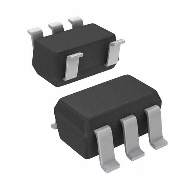
| 产品图片 |
|
| 产品型号 | SN74AUP1G126DBVR |
| PCN设计/规格 | |
| rohs | 无铅 / 符合限制有害物质指令(RoHS)规范要求 |
| 产品系列 | 74AUP |
| 产品目录页面 | |
| 供应商器件封装 | SOT-23-5 |
| 元件数 | 1 |
| 其它名称 | 296-18005-6 |
| 包装 | Digi-Reel® |
| 安装类型 | 表面贴装 |
| 封装/外壳 | SC-74A,SOT-753 |
| 工作温度 | -40°C ~ 85°C |
| 标准包装 | 1 |
| 每元件位数 | 1 |
| 电压-电源 | 0.8 V ~ 3.6 V |
| 电流-输出高,低 | 4mA,4mA |
| 逻辑类型 | 缓冲器/线路驱动器,非反相 |


PDF Datasheet 数据手册内容提取
Product Order Technical Tools & Support & Folder Now Documents Software Community SN74AUP1G126 SCES596G–JULY2004–REVISEDAUGUST2017 SN74AUP1G126 Low-Power Single Bus Buffer Gate With Tri-State Output 1 Features 3 Description • Latch-UpPerformanceExceeds100mAPer The AUP family is TI's premier solution to the 1 industry's low-power needs in battery-powered JESD78,ClassII portable applications. This family assures a very low • ESDPerformanceTestedPerJESD22− static and dynamic power consumption across the – 2000-VHuman-BodyModel entire V range of 0.8 V to 3.6 V, resulting in an CC (A114-B,ClassII) increased battery life. This product also maintains excellent signal integrity (see AUP – The Lowest- – 1000-VCharged-DeviceModel(C101) PowerFamilyandExcellentSignalIntegrity ). • AvailableintheTexasInstruments NanoStar™ Package This bus buffer gate is a single line driver with a 3- state output. The output is disabled when the output- • LowStatic-PowerConsumption enable (OE) input is low. This device has the input- (I =0.9µAMaximum) CC disablefeature,whichallowsfloatinginputsignals. • LowDynamic-PowerConsumption To assure the high-impedance state during power up (C =4pFTypicalat3.3V) pd or power down, OE should be tied to GND through a • LowInputCapacitance(Ci=1.5pFTypical) pulldownresistor;theminimumvalueoftheresistoris • LowNoise–OvershootandUndershoot determined by the current-sourcing capability of the <10%ofV driver. CC • Input-DisableFeatureAllowsFloatingInput NanoStar™ package technology is a major Conditions breakthrough in IC packaging concepts, using the die • I SupportsPartial-Power-DownModeOperation asthepackage. off • InputHysteresisAllowsSlowInputTransitionand This device is fully specified for partial-power-down BetterSwitchingNoiseImmunityatInput applications using I . The I circuitry disables the off off outputs when the device is powered down. This • WideOperatingV Rangeof0.8Vto3.6V CC inhibits current backflow into the device which • Optimizedfor3.3-VOperation preventsdamagetothedevice. • 3.6-VI/OToleranttoSupportMixed-ModeSignal Operation DeviceInformation(1) • t =4.6nsMaximumat3.3V PARTNUMBER PACKAGE BODYSIZE(NOM) pd • SuitableforPoint-to-PointApplications SN74AUP1G126DRL SOT-5X3(5) 1.60mm×1.20mm SN74AUP1G126DBV SOT-23(5) 1.60mm×2.90mm 2 Applications SN74AUP1G126DCK SC70(5) 1.25mm×2.00mm • AudioDock:Portable SN74AUP1G126DRY SON(6) 1.00mm×1.45mm • BluRay™PlayersandHomeTheaters SN74AUP1G126DSF SON(6) 1.00mm×1.00mm SN74AUP1G126YFP DSBGA(6) 0.76mm×1.16mm • PersonalDigitalAssistant(PDA) SN74AUP1G126YZP DSBGA(5) 0.89mm×1.39mm • Power:Telecom/ServerAC/DCSupply:Single SN74AUP1G126DPW X2SON(5) 0.80mm×0.80mm Controller:AnalogandDigital • Solid-StateDrive(SSD):ClientandEnterprise (1) For all available packages, see the orderable addendum at theendofthedatasheet. • TV:LCD/DigitalandHigh-Definition(HDTV) • Tablet:Enterprise LogicDiagram(PositiveLogic) • WirelessHeadsets,Keyboards,andMice 1 OE A 2 4 Y 1 An IMPORTANT NOTICE at the end of this data sheet addresses availability, warranty, changes, use in safety-critical applications, intellectualpropertymattersandotherimportantdisclaimers.PRODUCTIONDATA.
SN74AUP1G126 SCES596G–JULY2004–REVISEDAUGUST2017 www.ti.com Table of Contents 1 Features.................................................................. 1 8 DetailedDescription............................................ 14 2 Applications........................................................... 1 8.1 Overview.................................................................14 3 Description............................................................. 1 8.2 FunctionalBlockDiagram.......................................14 4 RevisionHistory..................................................... 2 8.3 FeatureDescription.................................................14 8.4 DeviceFunctionalModes........................................15 5 PinConfigurationandFunctions......................... 3 9 ApplicationandImplementation........................ 16 6 Specifications......................................................... 4 9.1 ApplicationInformation............................................16 6.1 AbsoluteMaximumRatings......................................4 9.2 TypicalApplication..................................................16 6.2 ESDRatings..............................................................4 10 PowerSupplyRecommendations..................... 17 6.3 RecommendedOperatingConditions.......................4 6.4 ThermalInformation..................................................5 11 Layout................................................................... 17 6.5 ElectricalCharacteristics...........................................5 11.1 LayoutGuidelines.................................................17 6.6 SwitchingCharacteristics:C =5pF........................7 11.2 LayoutExample....................................................17 L 6.7 SwitchingCharacteristics:C =10pF......................8 12 DeviceandDocumentationSupport................. 18 L 6.8 SwitchingCharacteristics:C =15pF......................9 12.1 DocumentationSupport........................................18 L 6.9 SwitchingCharacteristics:C =30pF....................10 12.2 ReceivingNotificationofDocumentationUpdates18 L 6.10 OperatingCharacteristics......................................11 12.3 CommunityResources..........................................18 6.11 TypicalCharacteristics..........................................11 12.4 Trademarks...........................................................18 7 ParameterMeasurementInformation................12 12.5 ElectrostaticDischargeCaution............................18 7.1 (PropagationDelays,SetupandHoldTimes,and 12.6 Glossary................................................................18 PulseWidth).............................................................12 13 Mechanical,Packaging,andOrderable 7.2 (EnableandDisableTimes)....................................13 Information........................................................... 18 4 Revision History NOTE:Pagenumbersforpreviousrevisionsmaydifferfrompagenumbersinthecurrentversion. ChangesfromRevisionF(May2010)toRevisionG Page • AddedDeviceInformationtable,PinConfigurationandFunctionssection,ESDRatingstable,ThermalInformation table,FeatureDescriptionsection,ApplicationandImplementationsection,Layoutsection,Deviceand DocumentationSupportsection,andMechanical,Packaging,andOrderableInformationsection....................................... 1 • DeletedOrderingInformationtable,seeMechanical,Packaging,andOrderableInformationattheendofthedata sheet ...................................................................................................................................................................................... 1 2 SubmitDocumentationFeedback Copyright©2004–2017,TexasInstrumentsIncorporated ProductFolderLinks:SN74AUP1G126
SN74AUP1G126 www.ti.com SCES596G–JULY2004–REVISEDAUGUST2017 5 Pin Configuration and Functions DBVPackage 5-PinSOT-23 DKCPackage TopView 5-PinSOT-23 TopView OE 1 5 V OE 1 5 V CC CC A 2 A 2 GND 3 4 Y GND 3 4 Y DRLPackage 5-PinSOT-5X3 DPWPackage TopView 5-PinX2SON TopView OE 1 5 V CC OE V GND CC A 2 A Y GGNNDD 3 4 Y DRYPackage 6-PinSON DSFPackage TopView 6-PinSON TopView OE 1 6 V CC OE 1 6 V CC A 2 5 N.C. A 2 5 N.C. GND 3 4 Y GND 3 4 Y N.C.–Nointernalconnection. Seemechanicaldrawingsfordimensions. YFPPackage 6-PinDSBGA YZPPackage BottomView 5-PinDSBGA BottomView 1 2 1 2 C GND Y C GND Y B A DNU B A A OE VCC A OE VCC Not to scale Not to scale PinFunctions PIN DBV,DCK, DRY, I/O DESCRIPTION NAME YFP YZP DRL,DPW DSF A 2 2 B1 B1 I Input DNU — — — B2 — Donotuse GND 3 3 C1 C1 — Ground N.C. — 5 B2 — — NoInternalConnection OE 1 1 A1 A1 I Outputenable(activehigh) V 5 6 A2 A2 — Positivesupply CC Y 4 4 C2 C2 O Bufferedoutput Copyright©2004–2017,TexasInstrumentsIncorporated SubmitDocumentationFeedback 3 ProductFolderLinks:SN74AUP1G126
SN74AUP1G126 SCES596G–JULY2004–REVISEDAUGUST2017 www.ti.com 6 Specifications 6.1 Absolute Maximum Ratings overoperatingfree-airtemperaturerange(unlessotherwisenoted)(1) MIN MAX UNIT V Supplyvoltage –0.5 4.6 V CC V Inputvoltage(2) –0.5 4.6 V I V Voltagerangeappliedtoanyoutputinthehigh-impedanceorpower-offstate(2) –0.5 4.6 V O V Outputvoltagerangeinthehighorlowstate(2) –0.5 V +0.5 V O CC I Inputclampcurrent V <0 –50 mA IK I I Outputclampcurrent V <0 –50 mA OK O I Continuousoutputcurrent ±20 mA O ContinuouscurrentthroughV orGND ±50 mA CC T JunctionTemperature 150 °C j T Storagetemperature –65 150 °C stg (1) StressesbeyondthoselistedunderAbsoluteMaximumRatingsmaycausepermanentdamagetothedevice.Thesearestressratings only,whichdonotimplyfunctionaloperationofthedeviceattheseoranyotherconditionsbeyondthoseindicatedunderRecommended OperatingConditions.Exposuretoabsolute-maximum-ratedconditionsforextendedperiodsmayaffectdevicereliability. (2) Theinputnegative-voltageandoutputvoltageratingsmaybeexceedediftheinputandoutputcurrentratingsareobserved. 6.2 ESD Ratings VALUE UNIT Human-bodymodel(HBM),perANSI/ESDA/JEDECJS-001(1) 2000 V Electrostaticdischarge V (ESD) Charged-devicemodel(CDM),perJEDECspecificationJESD22-C101(2) 1000 (1) JEDECdocumentJEP155statesthat500-VHBMallowssafemanufacturingwithastandardESDcontrolprocess. (2) JEDECdocumentJEP157statesthat250-VCDMallowssafemanufacturingwithastandardESDcontrolprocess. 6.3 Recommended Operating Conditions See(1) MIN MAX UNIT V Supplyvoltage 0.8 3.6 V CC V =0.8V V 3.6 CC CC V =1.1Vto1.95V 0.65×V 3.6 CC CC V High-levelinputvoltage V IH V =2.3Vto2.7V 1.6 3.6 CC V =3Vto3.6V 2 3.6 CC V =0.8V 0 CC V =1.1Vto1.95V 0 0.35×V CC CC V Low-levelinputvoltage V IL V =2.3Vto2.7V 0 0.7 CC V =3Vto3.6V 0 0.9 CC Activestate 0 V CC V Outputvoltage V O 3-state 0 3.6 V =0.8V –20 µA CC V =1.1V –1.1 CC V =1.4V –1.7 CC I High-leveloutputcurrent OH V =1.65V –1.9 mA CC V =2.3V –3.1 CC V =3V –4 CC (1) AllunusedinputsofthedevicemustbeheldatV orGNDtoassureproperdeviceoperation.SeeImplicationsofSlowofFloating CC CMOSInputs. 4 SubmitDocumentationFeedback Copyright©2004–2017,TexasInstrumentsIncorporated ProductFolderLinks:SN74AUP1G126
SN74AUP1G126 www.ti.com SCES596G–JULY2004–REVISEDAUGUST2017 Recommended Operating Conditions (continued) See(1) MIN MAX UNIT V =0.8V 20 µA CC V =1.1V 1.1 CC V =1.4V 1.7 CC I Low-leveloutputcurrent OL V =1.65V 1.9 mA CC V =2.3V 3.1 CC V =3V 4 CC Δt/Δv Inputtransitionriseorfallrate V =0.8Vto3.6V 200 ns/V CC T Operatingfree-airtemperature –40 85 °C A 6.4 Thermal Information SN74AUP1G126 THERMALMETRIC(1) DRL DBV DCK DRY DSF DPW YFP YZP UNIT (SOT-5X3) (SOT-23) (SC70) (SON) (SON) (X2SON) (DSBGA) (DSBGA) 5PINS 5PINS 5PINS 6PINS 6PINS 5PINS 6PINS 5PINS Junction-to-ambientthermal RθJA resistance 295.1 230.5 303.6 342.1 377.1 504.3 125.4 146.2 °C/W Junction-to-case(top)thermal RθJC(top) resistance 131.0 172.7 203.8 233.1 187.7 234.9 1.9 1.4 °C/W Junction-to-boardthermal RθJB resistance 143.9 62.2 100.9 206.7 236.6 370.3 37.2 39.3 °C/W Junction-to-top ψJT characterizationparameter 14.7 49.3 76.1 63.4 29.0 44.5 0.5 0.7 °C/W Junction-to-board ψJB characterizationparameter 144.4 61.6 99.3 206.7 236.3 369.7 37.5 39.8 °C/W Junction-to-case(bottom) RθJC(bot) thermalresistance N/A N/A N/A N/A N/A 165.2 N/A N/A °C/W (1) Formoreinformationabouttraditionalandnewthermalmetrics,seetheSemiconductorandICPackageThermalMetricsapplication report. 6.5 Electrical Characteristics overrecommendedoperatingfree-airtemperaturerange(unlessotherwisenoted) PARAMETER TESTCONDITIONS V MIN TYP MAX UNIT CC T =25°C V –0.1 A CC I =–20µA 0.8Vto3.6V OH T =–40°Cto+85°C V –0.1 A CC T =25°C 0.75×V A CC I =–1.1mA 1.1V OH T =–40°Cto+85°C 0.7×V A CC T =25°C 1.11 A I =–1.7mA 1.4V OH T =–40°Cto+85°C 1.03 A T =25°C 1.32 A I =–1.9mA 1.65V OH T =–40°Cto+85°C 1.3 A V V OH T =25°C 2.05 A I =–2.3mA OH T =–40°Cto+85°C 1.97 A 2.3V T =25°C 1.9 A I =–3.1mA OH T =–40°Cto+85°C 1.85 A T =25°C 2.72 A I =–2.7mA OH T =–40°Cto+85°C 2.67 A 3V T =25°C 2.6 A I =–4mA OH T =–40°Cto+85°C 2.55 A Copyright©2004–2017,TexasInstrumentsIncorporated SubmitDocumentationFeedback 5 ProductFolderLinks:SN74AUP1G126
SN74AUP1G126 SCES596G–JULY2004–REVISEDAUGUST2017 www.ti.com Electrical Characteristics (continued) overrecommendedoperatingfree-airtemperaturerange(unlessotherwisenoted) PARAMETER TESTCONDITIONS V MIN TYP MAX UNIT CC T =25°C 0.1 A I =20µA 0.8Vto3.6V OL T =–40°Cto+85°C 0.1 A T =25°C 0.3×V A CC I =1.1mA 1.1V OL T =–40°Cto+85°C 0.3×V A CC T =25°C 0.31 A I =1.7mA 1.4V OL T =–40°Cto+85°C 0.37 A T =25°C 0.31 A I =1.9mA 1.65V OL T =–40°Cto+85°C 0.35 A V V OL T =25°C 0.31 A I =2.3mA OL T =–40°Cto+85°C 0.33 A 2.3V T =25°C 0.44 A I =3.1mA OL T =–40°Cto+85°C 0.45 A T =25°C 0.31 A I =2.7mA OL T =–40°Cto+85°C 0.33 A 3V T =25°C 0.44 A I =4mA OL T =–40°Cto+85°C 0.45 A AorOE TA=25°C 0.1 I V =GNDto3.6V 0Vto3.6V µA I input I T =–40°Cto+85°C 0.5 A T =25°C 0.2 A I V orV =0Vto3.6V 0V µA off I O T =–40°Cto+85°C 0.6 A T =25°C 0.2 A ΔI V orV =0Vto3.6V 0Vto0.2V µA off I O T =–40°Cto+85°C 0.6 A I V =V orGND,T =–40°Cto+85°C 3.6V 0.5 µA OZ O CC A I VI=GNDor(VCCto3.6V), TA=25°C 0.8Vto3.6V 0.5 µA CC OE=GND,IO=0 TA=–40°Cto+85°C 0.9 T =25°C 40 A Ainput VI=VCC–0.6V(1), TA=–40°Cto+85°C 3.3V 50 ΔICC OEinput IO=0 TA=25°C 110 µA T =–40°Cto+85°C 120 A V =GNDto3.6V, Allinputs OIE=V (2),T =25°CorT =–40°Cto+85°C 0.8Vto3.6V 0 CC A A 0V 1.5 C V =V orGND,T =25°C pF i I CC A 3.6V 1.5 C V =V orGND,T =25°C 3.6V 3 pF o O CC A (1) OneinputatV –0.6V,otherinputatV orGND CC CC (2) ToshowI isverylowwhentheinput-disablefeatureisenabled CC 6 SubmitDocumentationFeedback Copyright©2004–2017,TexasInstrumentsIncorporated ProductFolderLinks:SN74AUP1G126
SN74AUP1G126 www.ti.com SCES596G–JULY2004–REVISEDAUGUST2017 6.6 Switching Characteristics: C = 5 pF L overrecommendedoperatingfree-airtemperaturerange,C =5pF(unlessotherwisenoted)(seeFigure2andFigure3) L FROM TO PARAMETER TESTCONDITIONS MIN TYP MAX UNIT (INPUT) (OUTPUT) V =0.8V T =25°C 18.1 CC A T =25°C 4.3 7.4 12.6 A V =1.2V±0.1V CC T =–40°Cto+85°C 2.7 15.3 A T =25°C 3.3 5.2 8.5 A V =1.5V±0.1V CC T =–40°Cto+85°C 1 10.2 A t A Y T =25°C 2.6 4.1 6.8 ns pd A V =1.8V±0.15V CC T =–40°Cto+85°C 1.3 8.3 A T =25°C 2 2.9 4.7 A V =2.5V±0.2V CC T =–40°Cto+85°C 1.1 5.8 A T =25°C 1.7 2.4 3.8 A V =3.3V±0.3V CC T =–40°Cto+85°C 1 4.6 A V =0.8V T =25°C 19.1 CC A T =25°C 5.1 9.3 15.9 A V =1.2V±0.1V CC T =–40°Cto+85°C 3.6 19.2 A T =25°C 4.1 6.6 10.5 A V =1.5V±0.1V CC T =–40°Cto+85°C 2.5 12.7 A t OE Y T =25°C 3.2 5.3 8.7 ns en A V =1.8V±0.15V CC T =–40°Cto+85°C 2.1 10.3 A T =25°C 2.5 3.8 6 A V =2.5V±0.2V CC T =–40°Cto+85°C 1.6 7.2 A T =25°C 2.1 3.2 4.9 A V =3.3V±0.3V CC T =–40°Cto+85°C 1.4 5.9 A V =0.8V T =25°C 12.1 CC A T =25°C 2.4 4.1 6.9 A V =1.2V±0.1V CC T =–40°Cto+85°C 2.2 7.7 A T =25°C 1.8 2.9 4.5 A V =1.5V±0.1V CC T =–40°Cto+85°C 1.7 5.1 A t OE Y T =25°C 1 2.9 4.3 ns dis A V =1.8V±0.15V CC T =–40°Cto+85°C 1.5 4.7 A T =25°C 1 1.8 2.7 A V =2.5V±0.2V CC T =–40°Cto+85°C 1 3.3 A T =25°C 1.2 2.2 3.2 A V =3.3V±0.3V CC T =–40°Cto+85°C 1.1 4 A Copyright©2004–2017,TexasInstrumentsIncorporated SubmitDocumentationFeedback 7 ProductFolderLinks:SN74AUP1G126
SN74AUP1G126 SCES596G–JULY2004–REVISEDAUGUST2017 www.ti.com 6.7 Switching Characteristics: C = 10 pF L overrecommendedoperatingfree-airtemperaturerange,C =10pF(unlessotherwisenoted)(seeFigure2andFigure3) L FROM TO PARAMETER TESTCONDITIONS MIN TYP MAX UNIT (INPUT) (OUTPUT) V =0.8V T =25°C 20.5 13.7 CC A T =25°C 4.6 8.4 9.3 A V =1.2V±0.1V CC T =–40°Cto+85°C 3.6 16.6 A T =25°C 3.5 5.9 7.5 A V =1.5V±0.1V CC T =–40°Cto+85°C 2.4 11.1 A t AorB Y T =25°C 3.9 4.7 5.3 ns pd A V =1.8V±0.15V CC T =–40°Cto+85°C 1.3 9.1 A T =25°C 2.3 3.4 4.3 A V =2.5V±0.2V CC T =–40°Cto+85°C 1.6 6.4 A T =25°C 2.1 2.8 A V =3.3V±0.3V CC T =–40°Cto+85°C 1.4 5.2 A V =0.8V T =25°C 21.8 16.8 CC A T =25°C 4.9 10.2 11.2 A V =1.2V±0.1V CC T =–40°Cto+85°C 4.4 20.2 A T =25°C 3.9 7.3 9.2 A V =1.5V±0.1V CC T =–40°Cto+85°C 3.3 13.5 A t OE Y T =25°C 3.4 5.8 6.4 ns en A V =1.8V±0.15V CC T =–40°Cto+85°C 2.7 11 A T =25°C 2.5 4.3 5.4 A V =2.5V±0.2V CC T =–40°Cto+85°C 2.1 7.8 A T =25°C 2.1 3.7 A V =3.3V±0.3V CC T =–40°Cto+85°C 1.9 6.4 A V =0.8V T =25°C 13 CC A T =25°C 3.8 6.6 11.7 A V =1.2V±0.1V CC T =–40°Cto+85°C 1.2 14 A T =25°C 2.2 4.7 7.9 A V =1.5V±0.1V CC T =–40°Cto+85°C 1.3 9.3 A t OE Y T =25°C 2.4 4.4 6.4 ns dis A V =1.8V±0.15V CC T =–40°Cto+85°C 2.2 7.5 A T =25°C 1.3 3.1 4.9 A V =2.5V±0.2V CC T =–40°Cto+85°C 1.2 5.4 A T =25°C 1.9 3.4 5 A V =3.3V±0.3V CC T =–40°Cto+85°C 1.9 5.6 A 8 SubmitDocumentationFeedback Copyright©2004–2017,TexasInstrumentsIncorporated ProductFolderLinks:SN74AUP1G126
SN74AUP1G126 www.ti.com SCES596G–JULY2004–REVISEDAUGUST2017 6.8 Switching Characteristics: C = 15 pF L overrecommendedoperatingfree-airtemperaturerange,C =15pF(unlessotherwisenoted)(seeFigure2andFigure3) L FROM TO PARAMETER TESTCONDITIONS MIN TYP MAX UNIT (INPUT) (OUTPUT) V =0.8V T =25°C 22.5 CC A T =25°C 5.8 9.3 15.1 A V =1.2V±0.1V CC T =–40°Cto+85°C 4.3 17.9 A T =25°C 4.4 6.6 10.2 A V =1.5V±0.1V CC T =–40°Cto+85°C 3 12.1 A t AorB Y T =25°C 3.5 5.3 8.3 ns pd A V =1.8V±0.15V CC T =–40°Cto+85°C 2.3 9.9 A T =25°C 2.7 3.9 5.8 A V =2.5V±0.2V CC T =–40°Cto+85°C 1.9 7 A T =25°C 2.4 3.2 4.7 A V =3.3V±0.3V CC T =–40°Cto+85°C 1.8 5.7 A V =0.8V T =25°C 25.2 CC A T =25°C 7 11.3 18.1 A V =1.2V±0.1V CC T =–40°Cto+85°C 5.4 21.4 A T =25°C 5.5 8.1 12.2 A V =1.5V±0.1V CC T =–40°Cto+85°C 4.1 14.5 A t OE Y T =25°C 4.3 6.5 10.1 ns en A V =1.8V±0.15V CC T =–40°Cto+85°C 3.3 12 A T =25°C 3.4 4.8 7.1 A V =2.5V±0.2V CC T =–40°Cto+85°C 2.6 8.4 A T =25°C 2.9 4.1 5.9 A V =3.3V±0.3V CC T =–40°Cto+85°C 2.3 6.9 A V =0.8V T =25°C 14 CC A T =25°C 3.7 5.8 8.2 A V =1.2V±0.1V CC T =–40°Cto+85°C 3.3 11 A T =25°C 5.5 3.9 5.9 A V =1.5V±0.1V CC T =–40°Cto+85°C 2.1 8 A t OE Y T =25°C 3.3 4.5 6.6 ns dis A V =1.8V±0.15V CC T =–40°Cto+85°C 2.9 7.4 A T =25°C 2.3 3.2 4.3 A V =2.5V±0.2V CC T =–40°Cto+85°C 1.8 5.1 A T =25°C 2.4 4.8 6.2 A V =3.3V±0.3V CC T =–40°Cto+85°C 3.1 6.7 A Copyright©2004–2017,TexasInstrumentsIncorporated SubmitDocumentationFeedback 9 ProductFolderLinks:SN74AUP1G126
SN74AUP1G126 SCES596G–JULY2004–REVISEDAUGUST2017 www.ti.com 6.9 Switching Characteristics: C = 30 pF L overrecommendedoperatingfree-airtemperaturerange,C =30pF(unlessotherwisenoted)(seeFigure2andFigure3) L FROM TO PARAMETER TESTCONDITIONS MIN TYP MAX UNIT (INPUT) (OUTPUT) V =0.8V T =25°C 29 CC A T =25°C 7.4 12 18.7 A V =1.2V±0.1V CC T =–40°Cto+85°C 6.6 21.4 A T =25°C 5.7 8.6 12.5 A V =1.5V±0.1V CC T =–40°Cto+85°C 4.9 14.7 A t AorB Y T =25°C 4.8 6.9 10.1 ns pd A V =1.8V±0.15V CC T =–40°Cto+85°C 3.1 12 A T =25°C 3.9 5.1 7.2 A V =2.5V±0.2V CC T =–40°Cto+85°C 3.3 8.7 A T =25°C 3.5 4.8 6 A V =3.3V±0.3V CC T =–40°Cto+85°C 3 7 A V =0.8V T =25°C 33.4 CC A T =25°C 8.8 14.1 21.8 A V =1.2V±0.1V CC T =–40°Cto+85°C 7.4 25.5 A T =25°C 6.9 10.1 14.6 A V =1.5V±0.1V CC T =–40°Cto+85°C 5.6 17.4 A t OE Y T =25°C 5.6 8.1 12 ns en A V =1.8V±0.15V CC T =–40°Cto+85°C 4.7 14.1 A T =25°C 4.3 6.1 8.5 A V =2.5V±0.2V CC T =–40°Cto+85°C 3.8 10 A T =25°C 3.7 5.2 7.1 A V =3.3V±0.3V CC T =–40°Cto+85°C 3.4 8.3 A V =0.8V T =25°C 17.7 CC A T =25°C 5.8 10 16 A V =1.2V±0.1V CC T =–40°Cto+85°C 3.7 16 A T =25°C 5.7 7.7 10.9 A V =1.5V±0.1V CC T =–40°Cto+85°C 1 10.7 A t OE Y T =25°C 4.5 7.7 9.8 ns dis A V =1.8V±0.15V CC T =–40°Cto+85°C 4.4 12.5 A T =25°C 3.9 5.6 7.4 A V =2.5V±0.2V CC T =–40°Cto+85°C 3.2 9 A T =25°C 3.3 8.4 10.7 A V =3.3V±0.3V CC T =–40°Cto+85°C 6.6 10.8 A 10 SubmitDocumentationFeedback Copyright©2004–2017,TexasInstrumentsIncorporated ProductFolderLinks:SN74AUP1G126
SN74AUP1G126 www.ti.com SCES596G–JULY2004–REVISEDAUGUST2017 6.10 Operating Characteristics T =25°C A PARAMETER TESTCONDITIONS V TYP UNIT CC 0.8V 3.8 1.2V±0.1V 3.7 1.5V±0.1V 3.7 Outputenabled f=10MHz 1.8V±0.15V 3.7 2.5V±0.2V 3.9 3.3V±0.3V 4 Powerdissipation C 0.8V 0 pF pd capacitance 1.2V±0.1V 0 1.5V±0.1V 0 Outputdisabled f=10MHz 1.8V±0.15V 0 2.5V±0.2V 0 2.5V±0.2V 0 3.3V±0.3V 0 6.11 Typical Characteristics 30 CL = 5pF 27.5 CL = 10pF 25 CL = 15pF 22.5 CL = 30pF 20 s) 17.5 n (D 15 P T 12.5 10 7.5 5 2.5 0 0.75 1.25 1.75 2.25 2.75 3.25 VCC (V) D001 Figure1.PropagationDelayvs.SupplyVoltageandLoadCapacitance Copyright©2004–2017,TexasInstrumentsIncorporated SubmitDocumentationFeedback 11 ProductFolderLinks:SN74AUP1G126
SN74AUP1G126 SCES596G–JULY2004–REVISEDAUGUST2017 www.ti.com 7 Parameter Measurement Information 7.1 (Propagation Delays, Setup and Hold Times, and Pulse Width) From Output Under Test 1 M(cid:13) CL (See Note A) Load Circut VCC = 0.8 V VC±C 0=. 11 .V2 V VC ±C =0 .11. 5V V V C±C 0=. 115.8 V V VC ±C =0 .22. 5V V VC ±C =0 .33. 3V V CL 5, 10, 15, 30 pF 5, 10, 15, 30 pF 5, 10, 15, 30 pF 5, 10, 15, 30 pF 5, 10, 15, 30 pF 5, 10, 15, 30 pF VM VCC / 2 VCC / 2 VCC / 2 VCC / 2 VCC / 2 VCC / 2 VI VCC VCC VCC VCC VCC VCC tw VCC Input VCC / 2 VCC / 2 VI 0 V Input VM VM Voltage Waveforms 0 V Pulse Duration tPLH tPLH VOH Output VM VM VOL Timing Input VCC / 2 VCC 0 V tPLH tPLH Output VOH tsu th VM VM VCC VOL Data Input VCC / 2 VCC / 2 Voltage Waveforms Propagation Delay 0 V Voltage Waveforms Times Inverting and Noninverting Outputs Setup and Hold Times Notes: A. CL includes probe and jig capacitance. B. All input pulses are supplied by generators having the following characteristics: 355(cid:3)(cid:148)(cid:3)10 MHz, ZO = 50 (cid:13), tr / tf = 3 ns. C. The outputs are measured one at a time, with one transition per measurement. D. tPLH And tPHL Are the same as Tpd. E. All parameters and waveforms are not applicable in all devices. Figure2. LoadCircuitandVoltageWaveforms 12 SubmitDocumentationFeedback Copyright©2004–2017,TexasInstrumentsIncorporated ProductFolderLinks:SN74AUP1G126
SN74AUP1G126 www.ti.com SCES596G–JULY2004–REVISEDAUGUST2017 7.2 (Enable and Disable Times) From Output 5 k(cid:13) S1 2 X VCC Under Test GND 5 k(cid:13) CL (See Note A) Load Circut Test S1 tPLZ / tPZL 2 x VCC tPHZ / tPZH GND VCC = 0.8 V VC±C 0=. 11 .V2 V VC ±C =0 .11. 5V V V C±C 0=. 115.8 V V VC ±C =0 .22. 5V V VC ±C =0 .33. 3V V CL 5, 10, 15, 30 pF 5, 10, 15, 30 pF 5, 10, 15, 30 pF 5, 10, 15, 30 pF 5, 10, 15, 30 pF 5, 10, 15, 30 pF VVVMßI VVCCC C/ 2 VVCCC C/ 2 VVCCC C/ 2 VVCCC C/ 2 VVCCC C/ 2 VVCCC C/ 2 Vcc Output Control VCC / 2 VCC / 2 0 V Output Waveform 1 tPZL tPLZ S1 at 2 x VCC Vcc (See Note B) VCC / 2 VOL + Vß VOL tPZH tPHZ Outp2u tS W1 aavte GfoNrmD VCC / 2 VOH- Vß VOH (See Note B) §(cid:3)0 V Voltage Waveforms Propagation Delay Times Inverting and Noninverting Outputs Notes: A. CL includes probe and jig capacitance. B. Waveform 1 is for an output with internal conditions such that the output is low, except when disabled by the output control. Waveform 2 is for an output with internal conditions such tht the output is high, except when disabled by the output control. C. All input pulses are supplied by generators having the following characteristics: 355(cid:3)(cid:148)(cid:3)10 MHz, ZO= 50 (cid:13), tr / tf = 3 ns D. The outputs are measured one at a time, with one transmision per measurement. E. tPLZ and tPHZ are the same as tdis. F. tPZL and tPZH are the same as ten. G. All parameters and waveforms are not applicable to all devices. Figure3. LoadCircuitandVoltageWaveforms Copyright©2004–2017,TexasInstrumentsIncorporated SubmitDocumentationFeedback 13 ProductFolderLinks:SN74AUP1G126
SN74AUP1G126 SCES596G–JULY2004–REVISEDAUGUST2017 www.ti.com 8 Detailed Description 8.1 Overview The AUP family is TI's premier solution to the industry's low-power needs in battery-powered portable applications. This family of devices is specified for low static and dynamic power consumption across the entire V range of 0.8 V to 3.6 V, resulting in an increased battery life. This product also maintains excellent signal CC integrity(seeFigure7andFigure8). The SN74AUP1G126 device contains one buffer gate device with output enable control and performs the Boolean function Y = A. This device is fully specified for partial-power-down applications using I . The I off off circuitry disables the outputs when the device is powered down. This inhibits current backflow into the device whichpreventsdamagetothedevice. To assure the high-impedance state during power up or power down, OE must be tied to GND through a pullup resistor;theminimumvalueoftheresistorisdeterminedbythecurrent-sinkingcapabilityofthedriver. 8.2 Functional Block Diagram 1 OE 2 4 A Y Figure4. LogicDiagram(PositiveLogic) 8.3 Feature Description 8.3.1 BalancedCMOSPush-PullOutputs A balanced output allows the device to sink and source similar currents. The drive capability of this device creates fast edges into light loads so routing and load conditions should be considered to prevent ringing. Additionally, the outputs of this device are capable of driving larger currents than the device can sustain without being damaged. It is important for the power output of the device to be limited to avoid thermal runaway and damage due to over-current. The electrical and thermal limits defined the in the Absolute Maximum Ratings must befollowedatalltimes. 8.3.2 StandardCMOSInputs Standard CMOS inputs are high impedance and are typically modelled as a resistor in parallel with the input capacitance given in the Electrical Characteristics. The worst case resistance is calculated with the maximum input voltage, given in the Absolute Maximum Ratings, and the maximum input leakage current, given in the ElectricalCharacteristics,usingohm'slaw(R=V ÷ I). Signals applied to the inputs must have fast edge rates, as defined by Δt/Δv in Recommended Operating Conditions to avoid excessive currents and oscillations. If a slow or noisy input signal is required, a device with a Schmitt-triggerinputshouldbeusedtoconditiontheinputsignalpriortothestandardCMOSinput. 14 SubmitDocumentationFeedback Copyright©2004–2017,TexasInstrumentsIncorporated ProductFolderLinks:SN74AUP1G126
SN74AUP1G126 www.ti.com SCES596G–JULY2004–REVISEDAUGUST2017 Feature Description (continued) 8.3.3 ClampDiodes Theinputsandoutputstothisdevicehavenegativeclampingdiodes. CAUTION Voltages beyond the values specified in the Absolute Maximum Ratings table can cause damage to the device. The input negative-voltage and output voltage ratings maybeexceedediftheinputandoutputclamp-currentratingsareobserved. Device VCC Input Logic Output -IIK -IOK GND Figure5. ElectricalPlacementofClampingDiodesforEachInputandOutput 8.3.4 PartialPowerDown(I ) off The inputs and outputs for this device enter a high-impedance state when the supply voltage is 0 V. The maximum leakage into or out of any input or output pin on the device is specified by I in the Electrical off Characteristics. 8.3.5 OvervoltageTolerantInputs Input signals to this device can be driven above the supply voltage so long as they remain below the maximum inputvoltagevaluespecifiedintheAbsoluteMaximumRatings. 8.3.6 OutputEnable This device has an output enable (OE) pin that functions according to Table 1. When the outputs of the device are disabled, they are placed into a high impedance state where it will neither source nor sink current. High- impedance outputs are also commonly referred to as three-state or tri-state outputs. The maximum leakage for theoutputinthisstateisdefinedbyI intheElectricalCharacteristicstable. OZ 8.4 Device Functional Modes Table1liststhefunctionalmodesoftheSN74AUP1G126device. Table1.FunctionTable INPUTS OUTPUT Y OE A H H H H L L L X Z Copyright©2004–2017,TexasInstrumentsIncorporated SubmitDocumentationFeedback 15 ProductFolderLinks:SN74AUP1G126
SN74AUP1G126 SCES596G–JULY2004–REVISEDAUGUST2017 www.ti.com 9 Application and Implementation NOTE Information in the following applications sections is not part of the TI component specification, and TI does not warrant its accuracy or completeness. TI’s customers are responsible for determining suitability of components for their purposes. Customers should validateandtesttheirdesignimplementationtoconfirmsystemfunctionality. 9.1 Application Information The SN74AUP1G126 device is an output enabled CMOS buffer that can be used in LED indicator applications that require less than 4 mA. The device can produce up to 4 mA of drive current at 3.3 V. The inputs to the devicearealsoovervoltagetolerantupto3.6V,allowingittotranslatedowntoanyvalidV . CC 9.2 Typical Application V CC V CC OE Override LED MCU Input A Y Indicator Output Figure6. ApplicationSchematicwithMCUdrivinganLEDIndicator 9.2.1 DesignRequirements ThisdeviceusesCMOStechnologyandhasbalancedoutputdrive.Takecaretoavoidbuscontentionbecauseit can drive currents that would exceed maximum limits. The output drive strength of this device creates fast edges intolightloadssoroutingandloadconditionsshouldbeconsideredtopreventringing. 9.2.2 DetailedDesignProcedure 1. RecommendedInputConditions – Risetimeandfalltimespecs.See(Δt/ΔV)intheRecommendedOperatingConditionstable. – Specifiedhighandlowlevels.See(V andV )intheRecommendedOperatingConditions table. IH IL – Inputs are overvoltage tolerant allowing them to go as high as (V max) in the Recommended Operating I ConditionstableatanyvalidV . CC 2. RecommendedOutputConditions – Load currents should not exceed (I max) per output and should not exceed (Continuous current through O V orGND)totalcurrentforthepart.TheselimitsarelocatedintheAbsoluteMaximumRatings table. CC – OutputsshouldnotbepulledaboveV . CC 9.2.3 ApplicationCurves 3.5 3 2.5 e - V1.25 Input Output g L3o.g3i-cV(1) L3o.g3i-cV(1) Volta .51 0 -0.5 0 5 10 15 20 25 30 35 40 45 Time - ns (1)AUP1G08 data at CL= 15 pF (1)Single,dual,and triple gates Figure8.ExcellentSignalIntegrity Figure7.AUP–TheLowest-PowerFamily 16 SubmitDocumentationFeedback Copyright©2004–2017,TexasInstrumentsIncorporated ProductFolderLinks:SN74AUP1G126
SN74AUP1G126 www.ti.com SCES596G–JULY2004–REVISEDAUGUST2017 10 Power Supply Recommendations The power supply can be any voltage between the minimum and maximum supply voltage rating located in the RecommendedOperatingConditionstable. The VCC pin must have a good bypass capacitor to prevent power disturbance. TI recommends to use a 0.1-µF capacitor for this device. It is ok to parallel multiple bypass caps to reject different frequencies of noise. 0.1-µF and 1-µF capacitors are commonly used in parallel. Install the bypass capacitor as close to the power pin as possibleforbestresults. 11 Layout 11.1 Layout Guidelines Even low data rate digital signals can contain high-frequency signal components due to fast edge rates. When a printed-circuit board (PCB) trace turns a corner at a 90° angle, a reflection can occur. A reflection occurs primarily because of the change of width of the trace. At the apex of the turn, the trace width increases to 1.414 times the width. This increase upsets the transmission-line characteristics, especially the distributed capacitance and self–inductance of the trace which results in the reflection. Not all PCB traces can be straight and therefore some traces must turn corners. shows progressively better techniques of rounding corners. Only the last example(BEST)maintainsconstanttracewidthandminimizesreflections. An example layout is given in for the DPW (X2SON-5) package. This example layout includes a 0402 (metric) capacitor and uses the measurements found in the example board layout appended to this end of this datasheet. A via of diameter 0.1 mm (3.973 mil) is placed directly in the center of the device. This via can be used to trace outthecenterpinconnectionthroughanotherboardlayer,oritcanbeleftoutofthelayout. 11.2 Layout Example WORST BETTER BEST W 2 1W min. W Figure9. TraceExample 0402 0.1 (cid:133)F Bypass Capacitor mil 4 8 mil 8 mil 8 mil SOLDER MASK OPENING, TYP METAL UNDER SOLDER MASK, TYP Figure10. ExampleLayoutWithDPW(X2SON-5)Package Copyright©2004–2017,TexasInstrumentsIncorporated SubmitDocumentationFeedback 17 ProductFolderLinks:SN74AUP1G126
SN74AUP1G126 SCES596G–JULY2004–REVISEDAUGUST2017 www.ti.com 12 Device and Documentation Support 12.1 Documentation Support 12.1.1 RelatedDocumentation Forrelateddocumentationseethefollowing: ImplicationsofSlowofFloatingCMOSInputs applicationreport 12.2 Receiving Notification of Documentation Updates To receive notification of documentation updates, navigate to the device product folder on ti.com. In the upper right corner, click on Alert me to register and receive a weekly digest of any product information that has changed.Forchangedetails,reviewtherevisionhistoryincludedinanyreviseddocument. 12.3 Community Resources The following links connect to TI community resources. Linked contents are provided "AS IS" by the respective contributors. They do not constitute TI specifications and do not necessarily reflect TI's views; see TI's Terms of Use. TIE2E™OnlineCommunity TI'sEngineer-to-Engineer(E2E)Community.Createdtofostercollaboration amongengineers.Ate2e.ti.com,youcanaskquestions,shareknowledge,exploreideasandhelp solveproblemswithfellowengineers. DesignSupport TI'sDesignSupport QuicklyfindhelpfulE2Eforumsalongwithdesignsupporttoolsand contactinformationfortechnicalsupport. 12.4 Trademarks NanoStar,E2EaretrademarksofTexasInstruments. BluRayisatrademarkofBlu-rayDiscAssociation(BDA). Allothertrademarksarethepropertyoftheirrespectiveowners. 12.5 Electrostatic Discharge Caution This integrated circuit can be damaged by ESD. Texas Instruments recommends that all integrated circuits be handled with appropriateprecautions.Failuretoobserveproperhandlingandinstallationprocedurescancausedamage. ESDdamagecanrangefromsubtleperformancedegradationtocompletedevicefailure.Precisionintegratedcircuitsmaybemore susceptibletodamagebecauseverysmallparametricchangescouldcausethedevicenottomeetitspublishedspecifications. 12.6 Glossary SLYZ022—TIGlossary. Thisglossarylistsandexplainsterms,acronyms,anddefinitions. 13 Mechanical, Packaging, and Orderable Information The following pages include mechanical, packaging, and orderable information. This information is the most current data available for the designated devices. This data is subject to change without notice and revision of thisdocument.Forbrowser-basedversionsofthisdatasheet,refertotheleft-handnavigation. 18 SubmitDocumentationFeedback Copyright©2004–2017,TexasInstrumentsIncorporated ProductFolderLinks:SN74AUP1G126
PACKAGE OPTION ADDENDUM www.ti.com 6-Feb-2020 PACKAGING INFORMATION Orderable Device Status Package Type Package Pins Package Eco Plan Lead/Ball Finish MSL Peak Temp Op Temp (°C) Device Marking Samples (1) Drawing Qty (2) (6) (3) (4/5) 74AUP1G126DRLRG4 ACTIVE SOT-5X3 DRL 5 4000 Green (RoHS NIPDAU Level-1-260C-UNLIM -40 to 85 (HN7, HNR) & no Sb/Br) SN74AUP1G126DBVR ACTIVE SOT-23 DBV 5 3000 Green (RoHS NIPDAU Level-1-260C-UNLIM -40 to 85 H26R & no Sb/Br) SN74AUP1G126DBVT ACTIVE SOT-23 DBV 5 250 Green (RoHS NIPDAU Level-1-260C-UNLIM -40 to 85 H26R & no Sb/Br) SN74AUP1G126DCKR ACTIVE SC70 DCK 5 3000 Green (RoHS NIPDAU Level-1-260C-UNLIM -40 to 85 (HN5, HNF, HNK, HN & no Sb/Br) R) SN74AUP1G126DCKT ACTIVE SC70 DCK 5 250 Green (RoHS NIPDAU Level-1-260C-UNLIM -40 to 85 (HN5, HNR) & no Sb/Br) SN74AUP1G126DPWR ACTIVE X2SON DPW 5 3000 Green (RoHS NIPDAU Level-1-260C-UNLIM -40 to 85 C4 & no Sb/Br) SN74AUP1G126DRLR ACTIVE SOT-5X3 DRL 5 4000 Green (RoHS NIPDAU | NIPDAUAG Level-1-260C-UNLIM -40 to 85 (HN7, HNR) & no Sb/Br) SN74AUP1G126DRYR ACTIVE SON DRY 6 5000 Green (RoHS NIPDAU Level-1-260C-UNLIM -40 to 85 HN & no Sb/Br) SN74AUP1G126DSFR ACTIVE SON DSF 6 5000 Green (RoHS NIPDAU | NIPDAUAG Level-1-260C-UNLIM -40 to 85 HN & no Sb/Br) SN74AUP1G126YFPR ACTIVE DSBGA YFP 6 3000 Green (RoHS SNAGCU Level-1-260C-UNLIM HNN & no Sb/Br) SN74AUP1G126YZPR ACTIVE DSBGA YZP 5 3000 Green (RoHS SNAGCU Level-1-260C-UNLIM -40 to 85 HNN & no Sb/Br) (1) The marketing status values are defined as follows: ACTIVE: Product device recommended for new designs. LIFEBUY: TI has announced that the device will be discontinued, and a lifetime-buy period is in effect. NRND: Not recommended for new designs. Device is in production to support existing customers, but TI does not recommend using this part in a new design. PREVIEW: Device has been announced but is not in production. Samples may or may not be available. OBSOLETE: TI has discontinued the production of the device. (2) RoHS: TI defines "RoHS" to mean semiconductor products that are compliant with the current EU RoHS requirements for all 10 RoHS substances, including the requirement that RoHS substance do not exceed 0.1% by weight in homogeneous materials. Where designed to be soldered at high temperatures, "RoHS" products are suitable for use in specified lead-free processes. TI may reference these types of products as "Pb-Free". RoHS Exempt: TI defines "RoHS Exempt" to mean products that contain lead but are compliant with EU RoHS pursuant to a specific EU RoHS exemption. Green: TI defines "Green" to mean the content of Chlorine (Cl) and Bromine (Br) based flame retardants meet JS709B low halogen requirements of <=1000ppm threshold. Antimony trioxide based flame retardants must also meet the <=1000ppm threshold requirement. Addendum-Page 1
PACKAGE OPTION ADDENDUM www.ti.com 6-Feb-2020 (3) MSL, Peak Temp. - The Moisture Sensitivity Level rating according to the JEDEC industry standard classifications, and peak solder temperature. (4) There may be additional marking, which relates to the logo, the lot trace code information, or the environmental category on the device. (5) Multiple Device Markings will be inside parentheses. Only one Device Marking contained in parentheses and separated by a "~" will appear on a device. If a line is indented then it is a continuation of the previous line and the two combined represent the entire Device Marking for that device. (6) Lead/Ball Finish - Orderable Devices may have multiple material finish options. Finish options are separated by a vertical ruled line. Lead/Ball Finish values may wrap to two lines if the finish value exceeds the maximum column width. Important Information and Disclaimer:The information provided on this page represents TI's knowledge and belief as of the date that it is provided. TI bases its knowledge and belief on information provided by third parties, and makes no representation or warranty as to the accuracy of such information. Efforts are underway to better integrate information from third parties. TI has taken and continues to take reasonable steps to provide representative and accurate information but may not have conducted destructive testing or chemical analysis on incoming materials and chemicals. TI and TI suppliers consider certain information to be proprietary, and thus CAS numbers and other limited information may not be available for release. In no event shall TI's liability arising out of such information exceed the total purchase price of the TI part(s) at issue in this document sold by TI to Customer on an annual basis. Addendum-Page 2
PACKAGE MATERIALS INFORMATION www.ti.com 2-Feb-2020 TAPE AND REEL INFORMATION *Alldimensionsarenominal Device Package Package Pins SPQ Reel Reel A0 B0 K0 P1 W Pin1 Type Drawing Diameter Width (mm) (mm) (mm) (mm) (mm) Quadrant (mm) W1(mm) SN74AUP1G126DBVR SOT-23 DBV 5 3000 180.0 8.4 3.23 3.17 1.37 4.0 8.0 Q3 SN74AUP1G126DBVT SOT-23 DBV 5 250 180.0 8.4 3.23 3.17 1.37 4.0 8.0 Q3 SN74AUP1G126DCKR SC70 DCK 5 3000 178.0 9.2 2.4 2.4 1.22 4.0 8.0 Q3 SN74AUP1G126DCKR SC70 DCK 5 3000 180.0 8.4 2.47 2.3 1.25 4.0 8.0 Q3 SN74AUP1G126DCKT SC70 DCK 5 250 180.0 8.4 2.47 2.3 1.25 4.0 8.0 Q3 SN74AUP1G126DCKT SC70 DCK 5 250 178.0 9.2 2.4 2.4 1.22 4.0 8.0 Q3 SN74AUP1G126DPWR X2SON DPW 5 3000 178.0 8.4 0.91 0.91 0.5 2.0 8.0 Q3 SN74AUP1G126DRLR SOT-5X3 DRL 5 4000 180.0 9.5 1.78 1.78 0.69 4.0 8.0 Q3 SN74AUP1G126DRLR SOT-5X3 DRL 5 4000 180.0 8.4 1.98 1.78 0.69 4.0 8.0 Q3 SN74AUP1G126DRYR SON DRY 6 5000 180.0 8.4 1.25 1.6 0.7 4.0 8.0 Q1 SN74AUP1G126DRYR SON DRY 6 5000 180.0 9.5 1.15 1.6 0.75 4.0 8.0 Q1 SN74AUP1G126DSFR SON DSF 6 5000 180.0 9.5 1.16 1.16 0.5 4.0 8.0 Q2 SN74AUP1G126YFPR DSBGA YFP 6 3000 178.0 9.2 0.89 1.29 0.62 4.0 8.0 Q1 SN74AUP1G126YZPR DSBGA YZP 5 3000 178.0 9.2 1.02 1.52 0.63 4.0 8.0 Q1 PackMaterials-Page1
PACKAGE MATERIALS INFORMATION www.ti.com 2-Feb-2020 *Alldimensionsarenominal Device PackageType PackageDrawing Pins SPQ Length(mm) Width(mm) Height(mm) SN74AUP1G126DBVR SOT-23 DBV 5 3000 202.0 201.0 28.0 SN74AUP1G126DBVT SOT-23 DBV 5 250 202.0 201.0 28.0 SN74AUP1G126DCKR SC70 DCK 5 3000 180.0 180.0 18.0 SN74AUP1G126DCKR SC70 DCK 5 3000 202.0 201.0 28.0 SN74AUP1G126DCKT SC70 DCK 5 250 202.0 201.0 28.0 SN74AUP1G126DCKT SC70 DCK 5 250 180.0 180.0 18.0 SN74AUP1G126DPWR X2SON DPW 5 3000 205.0 200.0 33.0 SN74AUP1G126DRLR SOT-5X3 DRL 5 4000 184.0 184.0 19.0 SN74AUP1G126DRLR SOT-5X3 DRL 5 4000 202.0 201.0 28.0 SN74AUP1G126DRYR SON DRY 6 5000 202.0 201.0 28.0 SN74AUP1G126DRYR SON DRY 6 5000 184.0 184.0 19.0 SN74AUP1G126DSFR SON DSF 6 5000 184.0 184.0 19.0 SN74AUP1G126YFPR DSBGA YFP 6 3000 220.0 220.0 35.0 SN74AUP1G126YZPR DSBGA YZP 5 3000 220.0 220.0 35.0 PackMaterials-Page2
PACKAGE OUTLINE DBV0005A SOT-23 - 1.45 mm max height SCALE 4.000 SMALL OUTLINE TRANSISTOR C 3.0 2.6 0.1 C 1.75 1.45 1.45 B A 0.90 PIN 1 INDEX AREA 1 5 2X 0.95 3.05 2.75 1.9 1.9 2 4 3 0.5 5X 0.3 0.15 0.2 C A B (1.1) TYP 0.00 0.25 GAGE PLANE 0.22 TYP 0.08 8 TYP 0.6 0 0.3 TYP SEATING PLANE 4214839/E 09/2019 NOTES: 1. All linear dimensions are in millimeters. Any dimensions in parenthesis are for reference only. Dimensioning and tolerancing per ASME Y14.5M. 2. This drawing is subject to change without notice. 3. Refernce JEDEC MO-178. 4. Body dimensions do not include mold flash, protrusions, or gate burrs. Mold flash, protrusions, or gate burrs shall not exceed 0.15 mm per side. www.ti.com
EXAMPLE BOARD LAYOUT DBV0005A SOT-23 - 1.45 mm max height SMALL OUTLINE TRANSISTOR PKG 5X (1.1) 1 5 5X (0.6) SYMM (1.9) 2 2X (0.95) 3 4 (R0.05) TYP (2.6) LAND PATTERN EXAMPLE EXPOSED METAL SHOWN SCALE:15X SOLDER MASK SOLDER MASK METAL UNDER METAL OPENING OPENING SOLDER MASK EXPOSED METAL EXPOSED METAL 0.07 MAX 0.07 MIN ARROUND ARROUND NON SOLDER MASK SOLDER MASK DEFINED DEFINED (PREFERRED) SOLDER MASK DETAILS 4214839/E 09/2019 NOTES: (continued) 5. Publication IPC-7351 may have alternate designs. 6. Solder mask tolerances between and around signal pads can vary based on board fabrication site. www.ti.com
EXAMPLE STENCIL DESIGN DBV0005A SOT-23 - 1.45 mm max height SMALL OUTLINE TRANSISTOR PKG 5X (1.1) 1 5 5X (0.6) SYMM 2 (1.9) 2X(0.95) 3 4 (R0.05) TYP (2.6) SOLDER PASTE EXAMPLE BASED ON 0.125 mm THICK STENCIL SCALE:15X 4214839/E 09/2019 NOTES: (continued) 7. Laser cutting apertures with trapezoidal walls and rounded corners may offer better paste release. IPC-7525 may have alternate design recommendations. 8. Board assembly site may have different recommendations for stencil design. www.ti.com
None
PACKAGE OUTLINE DPW0005A X2SON - 0.4 mm max height SCALE 12.000 PLASTIC SMALL OUTLINE - NO LEAD B 0.85 A 0.75 PIN 1 INDEX AREA 0.85 0.75 0.4 MAX C SEATING PLANE NOTE 3 (0.1) 0.05 (0.25) 4X (0.05) 0.00 0.25 0.1 2 4 NOTE 3 2X 3 2X (0.26) 0.48 5 1 0.27 0.27 4X 0.17 0.17 0.1 C A B (0.06) 0.05 C 0.32 3X 0.23 4223102/B 09/2017 NOTES: 1. All linear dimensions are in millimeters. Any dimensions in parenthesis are for reference only. Dimensioning and tolerancing per ASME Y14.5M. 2. This drawing is subject to change without notice. 3. The size and shape of this feature may vary. www.ti.com
EXAMPLE BOARD LAYOUT DPW0005A X2SON - 0.4 mm max height PLASTIC SMALL OUTLINE - NO LEAD (0.78) SYMM ( 0.1) 4X (0.42) VIA 0.05 MIN ALL AROUND 1 TYP 5 4X (0.22) SYMM 4X (0.26) (0.48) 3 2 4 (R0.05) TYP SOLDER MASK 4X (0.06) OPENING, TYP ( 0.25) (0.21) TYP METAL UNDER EXPOSED METAL SOLDER MASK CLEARANCE TYP LAND PATTERN EXAMPLE SOLDER MASK DEFINED SCALE:60X 4223102/B 09/2017 NOTES: (continued) 4. This package is designed to be soldered to a thermal pad on the board. For more information, refer to QFN/SON PCB application note in literature No. SLUA271 (www.ti.com/lit/slua271). www.ti.com
EXAMPLE STENCIL DESIGN DPW0005A X2SON - 0.4 mm max height PLASTIC SMALL OUTLINE - NO LEAD 4X (0.42) 4X (0.06) 5 4X (0.22) 1 ( 0.24) 4X (0.26) SYMM (0.21) (0.48) TYP SOLDER MASK 3 EDGE 2 4 (R0.05) TYP SYMM (0.78) SOLDER PASTE EXAMPLE BASED ON 0.1 mm THICK STENCIL EXPOSED PAD 92% PRINTED SOLDER COVERAGE BY AREA SCALE:100X 4223102/B 09/2017 NOTES: (continued) 5. Laser cutting apertures with trapezoidal walls and rounded corners may offer better paste release. IPC-7525 may have alternate design recommendations. www.ti.com
PACKAGE OUTLINE YZP0005 DSBGA - 0.5 mm max height SCALE 8.000 DIE SIZE BALL GRID ARRAY B E A BALL A1 CORNER D C 0.5 MAX SEATING PLANE 0.19 0.05 C 0.15 BALL TYP 0.5 TYP C SYMM 1 B D: Max = 1.418 mm, Min =1 .358 mm TYP 0.5 TYP E: Max = 0.918 mm, Min =0 .858 mm A 0.25 5X 1 2 0.21 0.015 C A B SYMM 4219492/A 05/2017 NOTES: 1. All linear dimensions are in millimeters. Any dimensions in parenthesis are for reference only. Dimensioning and tolerancing per ASME Y14.5M. 2. This drawing is subject to change without notice. www.ti.com
EXAMPLE BOARD LAYOUT YZP0005 DSBGA - 0.5 mm max height DIE SIZE BALL GRID ARRAY (0.5) TYP 5X ( 0.23) 1 2 A (0.5) TYP SYMM B C SYMM LAND PATTERN EXAMPLE SCALE:40X SOLDER MASK 0.05 MAX 0.05 MIN ( 0.23) OPENING SOLDER MASK OPENING ( 0.23) METAL METAL UNDER SOLDER MASK NON-SOLDER MASK SOLDER MASK DEFINED DEFINED (PREFERRED) SOLDER MASK DETAILS NOT TO SCALE 4219492/A 05/2017 NOTES: (continued) 3. Final dimensions may vary due to manufacturing tolerance considerations and also routing constraints. For more information, see Texas Instruments literature number SNVA009 (www.ti.com/lit/snva009). www.ti.com
EXAMPLE STENCIL DESIGN YZP0005 DSBGA - 0.5 mm max height DIE SIZE BALL GRID ARRAY (0.5) TYP 5X ( 0.25) (R0.05) TYP 1 2 A (0.5) TYP B SYMM C METAL SYMM TYP SOLDER PASTE EXAMPLE BASED ON 0.1 mm THICK STENCIL SCALE:40X 4219492/A 05/2017 NOTES: (continued) 4. Laser cutting apertures with trapezoidal walls and rounded corners may offer better paste release. www.ti.com
PACKAGE OUTLINE YFP0006 DSBGA - 0.5 mm max height SCALE 10.000 DIE SIZE BALL GRID ARRAY B E A BALL A1 CORNER D C 0.5 MAX SEATING PLANE 0.19 0.13 BALL TYP 0.05 C 0.4 TYP SYMM C D: Max = 1.19 mm, Min = 1.13 mm 0.8 TYP B SYMM E: Max = 0.79 mm, Min = 0.73 mm 0.4 TYP A 0.25 6X 0.21 1 2 0.015 C A B 4223410/A 11/2016 NOTES: 1. All linear dimensions are in millimeters. Any dimensions in parenthesis are for reference only. Dimensioning and tolerancing per ASME Y14.5M. 2. This drawing is subject to change without notice. www.ti.com
EXAMPLE BOARD LAYOUT YFP0006 DSBGA - 0.5 mm max height DIE SIZE BALL GRID ARRAY (0.4) TYP 6X ( 0.23) 1 2 A (0.4) TYP B SYMM C SYMM LAND PATTERN EXAMPLE SCALE:50X ( 0.23) 0.05 MAX 0.05 MIN METAL UNDER METAL SOLDER MASK SOLDER MASK ( 0.23) OPENING SOLDER MASK OPENING NON-SOLDER MASK SOLDER MASK DEFINED DEFINED (PREFERRED) SOLDER MASK DETAILS NOT TO SCALE 4223410/A 11/2016 NOTES: (continued) 3. Final dimensions may vary due to manufacturing tolerance considerations and also routing constraints. For more information, see Texas Instruments literature number SNVA009 (www.ti.com/lit/snva009). www.ti.com
EXAMPLE STENCIL DESIGN YFP0006 DSBGA - 0.5 mm max height DIE SIZE BALL GRID ARRAY (0.4) TYP 6X ( 0.25) (R0.05) TYP 1 2 A (0.4) TYP B SYMM METAL TYP C SYMM SOLDER PASTE EXAMPLE BASED ON 0.1 mm THICK STENCIL SCALE:50X 4223410/A 11/2016 NOTES: (continued) 4. Laser cutting apertures with trapezoidal walls and rounded corners may offer better paste release. www.ti.com
None
None
PACKAGE OUTLINE DSF0006A X2SON - 0.4 mm max height SCALE 10.000 PLASTIC SMALL OUTLINE - NO LEAD 1.05 B A 0.95 PIN 1 INDEX AREA 1.05 0.95 0.4 MAX C SEATING PLANE 0.05 C (0.11) TYP SYMM 0.05 0.00 3 4 2X SYMM 0.7 4X 0.35 6 1 0.22 6X 0.12 (0.1) PIN 1 ID 0.45 0.07 C B A 6X 0.35 0.05 C 4220597/A 06/2017 NOTES: 1. All linear dimensions are in millimeters. Any dimensions in parenthesis are for reference only. Dimensioning and tolerancing per ASME Y14.5M. 2. This drawing is subject to change without notice. 3. Reference JEDEC registration MO-287, variation X2AAF. www.ti.com
EXAMPLE BOARD LAYOUT DSF0006A X2SON - 0.4 mm max height PLASTIC SMALL OUTLINE - NO LEAD 6X (0.6) (R0.05) TYP 1 6X (0.17) 6 SYMM 4X (0.35) 4 3 SYMM (0.8) LAND PATTERN EXAMPLE EXPOSED METAL SHOWN SCALE:40X 0.07 MIN 0.07 MAX EXPOSED METAL ALL AROUND ALL AROUND EXPOSED METAL SOLDER MASK SOLDER MASK METAL METAL UNDER OPENING OPENING SOLDER MASK NON SOLDER MASK SOLDER MASK DEFINED DEFINED SOLDER MASK DETAILS 4220597/A 06/2017 NOTES: (continued) 4. For more information, see Texas Instruments literature number SLUA271 (www.ti.com/lit/slua271). www.ti.com
EXAMPLE STENCIL DESIGN DSF0006A X2SON - 0.4 mm max height PLASTIC SMALL OUTLINE - NO LEAD 6X (0.6) (R0.05) TYP 1 6X (0.17) 6 SYMM 4X (0.35) 4 3 SYMM (0.8) SOLDER PASTE EXAMPLE BASED ON 0.125 mm THICK STENCIL PRINTED SOLDER COVERAGE BY AREA UNDER PACKAGE SCALE:40X 4220597/A 06/2017 4. Laser cutting apertures with trapezoidal walls and rounded corners may offer better paste release. IPC-7525 may have alternate design recommendations. www.ti.com
None
None
GENERIC PACKAGE VIEW DRY 6 USON - 0.6 mm max height PLASTIC SMALL OUTLINE - NO LEAD Images above are just a representation of the package family, actual package may vary. Refer to the product data sheet for package details. 4207181/G
PACKAGE OUTLINE DRY0006A USON - 0.6 mm max height SCALE 8.500 PLASTIC SMALL OUTLINE - NO LEAD B 1.05 A 0.95 PIN 1 INDEX AREA 1.5 1.4 0.6 MAX C SEATING PLANE 0.05 0.00 0.08 C 3X 0.6 SYMM (0.127) TYP (0.05) TYP 3 4 4X 0.5 SYMM 2X 1 6 1 0.25 6X 0.15 0.4 0.3 0.1 C A B 0.05 C PIN 1 ID (OPTIONAL) 0.35 5X 0.25 4222894/A 01/2018 NOTES: 1. All linear dimensions are in millimeters. Any dimensions in parenthesis are for reference only. Dimensioning and tolerancing per ASME Y14.5M. 2. This drawing is subject to change without notice. www.ti.com
EXAMPLE BOARD LAYOUT DRY0006A USON - 0.6 mm max height PLASTIC SMALL OUTLINE - NO LEAD SYMM (0.35) 5X (0.3) 1 6 6X (0.2) SYMM 4X (0.5) 4 3 (R0.05) TYP (0.6) LAND PATTERN EXAMPLE 1:1 RATIO WITH PKG SOLDER PADS EXPOSED METAL SHOWN SCALE:40X 0.05 MAX 0.05 MIN ALL AROUND ALL AROUND EXPOSED EXPOSED METAL METAL SOLDER MASK METAL METAL UNDER SOLDER MASK OPENING SOLDER MASK OPENING NON SOLDER MASK DEFINED SOLDER MASK DEFINED (PREFERRED) SOLDER MASK DETAILS 4222894/A 01/2018 NOTES: (continued) 3. For more information, see QFN/SON PCB application report in literature No. SLUA271 (www.ti.com/lit/slua271). www.ti.com
EXAMPLE STENCIL DESIGN DRY0006A USON - 0.6 mm max height PLASTIC SMALL OUTLINE - NO LEAD SYMM (0.35) 5X (0.3) 1 6 6X (0.2) SYMM 4X (0.5) 4 3 (R0.05) TYP (0.6) SOLDER PASTE EXAMPLE BASED ON 0.075 - 0.1 mm THICK STENCIL SCALE:40X 4222894/A 01/2018 NOTES: (continued) 4. Laser cutting apertures with trapezoidal walls and rounded corners may offer better paste release. IPC-7525 may have alternate design recommendations. www.ti.com
IMPORTANTNOTICEANDDISCLAIMER TI PROVIDES TECHNICAL AND RELIABILITY DATA (INCLUDING DATASHEETS), DESIGN RESOURCES (INCLUDING REFERENCE DESIGNS), APPLICATION OR OTHER DESIGN ADVICE, WEB TOOLS, SAFETY INFORMATION, AND OTHER RESOURCES “AS IS” AND WITH ALL FAULTS, AND DISCLAIMS ALL WARRANTIES, EXPRESS AND IMPLIED, INCLUDING WITHOUT LIMITATION ANY IMPLIED WARRANTIES OF MERCHANTABILITY, FITNESS FOR A PARTICULAR PURPOSE OR NON-INFRINGEMENT OF THIRD PARTY INTELLECTUAL PROPERTY RIGHTS. These resources are intended for skilled developers designing with TI products. You are solely responsible for (1) selecting the appropriate TI products for your application, (2) designing, validating and testing your application, and (3) ensuring your application meets applicable standards, and any other safety, security, or other requirements. These resources are subject to change without notice. TI grants you permission to use these resources only for development of an application that uses the TI products described in the resource. Other reproduction and display of these resources is prohibited. No license is granted to any other TI intellectual property right or to any third party intellectual property right. TI disclaims responsibility for, and you will fully indemnify TI and its representatives against, any claims, damages, costs, losses, and liabilities arising out of your use of these resources. TI’s products are provided subject to TI’s Terms of Sale (www.ti.com/legal/termsofsale.html) or other applicable terms available either on ti.com or provided in conjunction with such TI products. TI’s provision of these resources does not expand or otherwise alter TI’s applicable warranties or warranty disclaimers for TI products. Mailing Address: Texas Instruments, Post Office Box 655303, Dallas, Texas 75265 Copyright © 2020, Texas Instruments Incorporated