ICGOO在线商城 > 集成电路(IC) > 逻辑 - 栅极和逆变器 > SN74AHCT86PWR

 Datasheet下载
- 型号: SN74AHCT86PWR
- 制造商: Texas Instruments
- 库位|库存: xxxx|xxxx
- 要求:
| 数量阶梯 | 香港交货 | 国内含税 |
| +xxxx | $xxxx | ¥xxxx |
查看当月历史价格
查看今年历史价格
SN74AHCT86PWR产品简介:
ICGOO电子元器件商城为您提供SN74AHCT86PWR由Texas Instruments设计生产,在icgoo商城现货销售,并且可以通过原厂、代理商等渠道进行代购。 SN74AHCT86PWR价格参考¥0.60-¥1.73。Texas InstrumentsSN74AHCT86PWR封装/规格:逻辑 - 栅极和逆变器, XOR (Exclusive OR) IC 4 Channel 14-TSSOP。您可以下载SN74AHCT86PWR参考资料、Datasheet数据手册功能说明书,资料中有SN74AHCT86PWR 详细功能的应用电路图电压和使用方法及教程。
| 参数 | 数值 |
| 产品目录 | 集成电路 (IC)半导体 |
| 描述 | IC GATE XOR 4CH 2-INP 14-TSSOP逻辑门 Quad 2 Input |
| 产品分类 | |
| 品牌 | Texas Instruments |
| 产品手册 | |
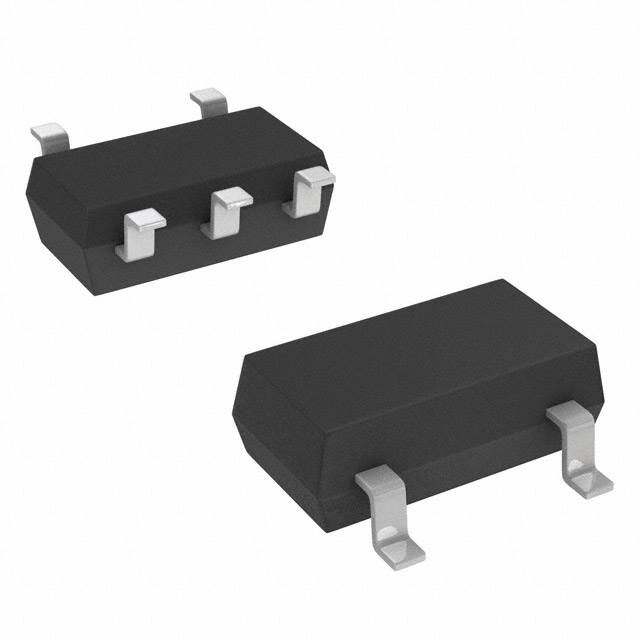
| 产品图片 |
|
| rohs | 符合RoHS无铅 / 符合限制有害物质指令(RoHS)规范要求 |
| 产品系列 | 逻辑集成电路,逻辑门,Texas Instruments SN74AHCT86PWR74AHCT |
| 数据手册 | |
| 产品型号 | SN74AHCT86PWR |
| 不同V、最大CL时的最大传播延迟 | 8.8ns @ 5V,50pF |
| 产品 | XOR |
| 产品目录页面 | |
| 产品种类 | 逻辑门 |
| 传播延迟时间 | 10 ns |
| 低电平输出电流 | 8 mA |
| 供应商器件封装 | 14-TSSOP |
| 其它名称 | 296-4778-2 |
| 包装 | 带卷 (TR) |
| 单位重量 | 57.200 mg |
| 商标 | Texas Instruments |
| 安装类型 | 表面贴装 |
| 安装风格 | SMD/SMT |
| 封装 | Reel |
| 封装/外壳 | 14-TSSOP(0.173",4.40mm 宽) |
| 封装/箱体 | TSSOP-14 |
| 工作温度 | -40°C ~ 85°C |
| 工作温度范围 | - 40 C to + 85 C |
| 工厂包装数量 | 2000 |
| 最大工作温度 | + 85 C |
| 最小工作温度 | - 40 C |
| 栅极数量 | 4 Gate |
| 标准包装 | 2,000 |
| 特性 | - |
| 电压-电源 | 4.5 V ~ 5.5 V |
| 电流-输出高,低 | 8mA,8mA |
| 电流-静态(最大值) | 2µA |
| 电源电压-最大 | 5.5 V |
| 电源电压-最小 | 4.5 V |
| 电路数 | 4 |
| 系列 | SN74AHCT86 |
| 输入/输出线数量 | 2 / 1 |
| 输入数 | 2 |
| 输入线路数量 | 2 |
| 输出线路数量 | 1 |
| 逻辑电平-低 | 0.8V |
| 逻辑电平-高 | 2V |
| 逻辑类型 | XOR(异或) |
| 逻辑系列 | AHCT |
| 高电平输出电流 | - 8 mA |


- 商务部:美国ITC正式对集成电路等产品启动337调查
- 曝三星4nm工艺存在良率问题 高通将骁龙8 Gen1或转产台积电
- 太阳诱电将投资9.5亿元在常州建新厂生产MLCC 预计2023年完工
- 英特尔发布欧洲新工厂建设计划 深化IDM 2.0 战略
- 台积电先进制程称霸业界 有大客户加持明年业绩稳了
- 达到5530亿美元!SIA预计今年全球半导体销售额将创下新高
- 英特尔拟将自动驾驶子公司Mobileye上市 估值或超500亿美元
- 三星加码芯片和SET,合并消费电子和移动部门,撤换高东真等 CEO
- 三星电子宣布重大人事变动 还合并消费电子和移动部门
- 海关总署:前11个月进口集成电路产品价值2.52万亿元 增长14.8%


PDF Datasheet 数据手册内容提取
Product Sample & Technical Tools & Support & Folder Buy Documents Software Community SN54AHCT86,SN74AHCT86 SCLS250N–OCTOBER1995–REVISEDAUGUST2014 SNx4AHCT86 Quadruple 2-Input Exclusive-OR Gates 1 Features 3 Description • InputsareTTL-VoltageCompatible The SNx4AHCT86 devices are quadruple 2-input 1 exclusive-OR gates. These devices perform the • Latch-UpPerformanceExceeds250mAPer Boolean function Y = A × B or Y = AB + AB in JESD17 positivelogic. • OnProductsComplianttoMIL-PRF-38535, AllParametersareTestedUnlessOtherwise DeviceInformation(1) Noted.OnAllOtherProducts,Production PARTNUMBER PACKAGE BODYSIZE(NOM) ProcessingDoesNotNecessarilyIncludeTesting TVSOP(14) 3.60mm×4.40mm ofAllParameters. SOIC(14) 8.65mm×3.91mm • ESDProtectionExceedsJESD22 SNx4AHCT574 SOP(14) 10.30mm×5.30mm – 2000-VHuman-BodyModel(A114-A) SSOP(14) 6.20mm×5.30mm – 200-VMachineModel(A115-A) TSSOP(14) 5.00mm×4.40mm (1) For all available packages, see the orderable addendum at 2 Applications theendofthedatasheet. • Server • PCsandNotebooks • NetworkSwitches • WearableHealthandFitnessDevices • TelecomInfrastructures • ElectronicPointsofSale 4 Simplified Schematic An exclusive-OR gate has many applications, some of which can be represented better by alternative logic symbols. EXCLUSIVE OR =1 These are five equivalent exclusive-OR symbols valid for an SN74AHCT86 gate in positive logic; negation may be shown at any twoports. LOGIC-IDENTITYELEMENT EVEN-PARITYELEMENT ODD-PARITYELEMENT = 2k 2k + 1 Theoutputisactive(low)if Theoutputisactive(low)if Theoutput is active (high)if allinputs stand at the same an even number of inputs an odd number of inputs logiclevel(thatis,A=B). (thatis,0or2)areactive. (that is, only 1 of the 2) are active. 1 An IMPORTANT NOTICE at the end of this data sheet addresses availability, warranty, changes, use in safety-critical applications, intellectualpropertymattersandotherimportantdisclaimers.PRODUCTIONDATA.
SN54AHCT86,SN74AHCT86 SCLS250N–OCTOBER1995–REVISEDAUGUST2014 www.ti.com Table of Contents 1 Features.................................................................. 1 9.1 Overview...................................................................8 2 Applications........................................................... 1 9.2 FunctionalBlockDiagram.........................................8 3 Description............................................................. 1 9.3 FeatureDescription...................................................8 9.4 DeviceFunctionalModes..........................................8 4 SimplifiedSchematic............................................. 1 10 ApplicationandImplementation.......................... 9 5 RevisionHistory..................................................... 2 10.1 ApplicationInformation............................................9 6 PinConfigurationandFunctions......................... 3 10.2 TypicalApplication .................................................9 7 Specifications......................................................... 4 11 PowerSupplyRecommendations..................... 10 7.1 AbsoluteMaximumRatings......................................4 12 Layout................................................................... 10 7.2 HandlingRatings.......................................................4 12.1 LayoutGuidelines.................................................10 7.3 RecommendedOperatingConditions.......................4 12.2 LayoutExample....................................................10 7.4 ThermalInformation..................................................5 13 DeviceandDocumentationSupport................. 11 7.5 ElectricalCharacteristics...........................................5 7.6 SwitchingCharacteristics..........................................5 13.1 RelatedLinks........................................................11 7.7 NoiseCharacteristics................................................6 13.2 Trademarks...........................................................11 7.8 OperatingCharacteristics..........................................6 13.3 ElectrostaticDischargeCaution............................11 7.9 TypicalCharacteristics..............................................6 13.4 Glossary................................................................11 8 ParameterMeasurementInformation..................7 14 Mechanical,Packaging,andOrderable Information........................................................... 11 9 DetailedDescription.............................................. 8 5 Revision History NOTE:Pagenumbersforpreviousrevisionsmaydifferfrompagenumbersinthecurrentversion. ChangesfromRevisionM(July2003)toRevisionN Page • UpdateddocumenttonewTIdatasheetformat.................................................................................................................... 1 • DeletedOrderingInformationtable........................................................................................................................................ 1 • AddedMilitaryDisclaimertoFeatureslist.............................................................................................................................. 1 • AddedApplications................................................................................................................................................................. 1 • AddedPinFunctionstable...................................................................................................................................................... 3 • AddedHandlingRatingstable................................................................................................................................................ 4 • ChangedMAXoperatingtemperatureto125°CinRecommendedOperatingConditionstable. ......................................... 4 • AddedThermalInformationtable........................................................................................................................................... 5 • Added–40°Cto125°CforSN74AHCT86intheElectricalCharacteristicstable................................................................... 5 • Added–40°Cto125°CforSN74AHCT86intheSwitchingCharacteristicstable.................................................................. 5 • AddedTypicalCharacteristics................................................................................................................................................ 6 • AddedDetailedDescriptionsection........................................................................................................................................ 8 • AddedApplicationandImplementationsection...................................................................................................................... 9 • AddedPowerSupplyRecommendationsandLayoutsections............................................................................................ 10 2 SubmitDocumentationFeedback Copyright©1995–2014,TexasInstrumentsIncorporated ProductFolderLinks:SN54AHCT86 SN74AHCT86
SN54AHCT86,SN74AHCT86 www.ti.com SCLS250N–OCTOBER1995–REVISEDAUGUST2014 6 Pin Configuration and Functions SN54AHCT86...JORWPACKAGE SN74AHCT86...RGYPACKAGE SN54AHCT86...FKPACKAGE SN74AHCT86...D, DB, DGV, N, NS, (TOPVIEW) (TOPVIEW) ORPWPACKAGE (TOPVIEW) 1A VCC 1B 1A NC VCC4B 1A 1 14 VCC 1B 2 1 14 13 4B 1Y 43 2 1 20 1918 4A 1B 2 13 4B 1Y 3 12 4A NC 5 17 NC 1Y 3 12 4A 2A 4 11 4Y 2A 6 16 4Y 2A 4 11 4Y 2B 5 10 3B NC 7 15 NC 2B 5 10 3B 2Y 6 9 3A 2B 8 14 3B 2Y 6 9 3A 9 10 11 12 13 7 8 GND 7 8 3Y D Y YD CY A N 3 2N N3 3 G G NC−No internal connection PinFunctions PIN SN74AHCT86 SN54AHCT86 I/O DESCRIPTION NAME D,DB,DGV, RGY J,W FK N,NS,PW 1A 1 1 1 2 I 1AInput 1B 2 2 2 3 I 1BInput 1Y 3 3 3 4 O 1YOutput 2A 4 4 4 6 I 2AInput 2B 5 5 5 8 I 2BInput 2Y 6 6 6 9 O 2YOutput 3Y 8 8 8 12 O 3YOutput 3A 9 9 9 13 I 3AInput 3B 10 10 10 14 I 3BInput 4Y 11 11 11 16 O 4YOutput 4A 12 12 12 18 I 4AInput 4B 13 13 13 19 I 4BInput GND 7 7 7 10 — GroundPin 1 5 7 NC — — — — NoConnection 11 15 17 V 14 14 14 20 — PowerPin CC Copyright©1995–2014,TexasInstrumentsIncorporated SubmitDocumentationFeedback 3 ProductFolderLinks:SN54AHCT86 SN74AHCT86
SN54AHCT86,SN74AHCT86 SCLS250N–OCTOBER1995–REVISEDAUGUST2014 www.ti.com 7 Specifications 7.1 Absolute Maximum Ratings overoperatingfree-airtemperaturerange(unlessotherwisenoted)(1) MIN MAX UNIT V Supplyvoltagerange –0.5 7 V CC V Inputvoltagerange(2) –0.5 7 V I V Outputvoltagerange(2) –0.5 V +0.5 V O CC I Inputclampcurrent V <0 –20 mA IK I I Outputclampcurrent V <0orV >V ±20 mA OK O O CC I Continuousoutputcurrent V =0toV ±25 mA O O CC ContinuouscurrentthroughV orGND ±50 mA CC (1) StressesbeyondthoselistedunderAbsoluteMaximumRatingsmaycausepermanentdamagetothedevice.Thesearestressratings only,andfunctionaloperationofthedeviceattheseoranyotherconditionsbeyondthoseindicatedunderRecommendedOperating Conditionsisnotimplied.Exposuretoabsolute-maximum-ratedconditionsforextendedperiodsmayaffectdevicereliability. (2) Theinputandoutputvoltageratingsmaybeexceedediftheinputandoutputcurrentratingsareobserved. 7.2 Handling Ratings MIN MAX UNIT T Storagetemperaturerange –65 150 °C stg Humanbodymodel(HBM),perANSI/ESDA/JEDECJS-001,all pins(1) 0 2000 V Electrostaticdischarge V (ESD) Chargeddevicemodel(CDM),perJEDECspecification JESD22-C101,allpins(2) 0 1000 (1) JEDECdocumentJEP155statesthat500-VHBMallowssafemanufacturingwithastandardESDcontrolprocess. (2) JEDECdocumentJEP157statesthat250-VCDMallowssafemanufacturingwithastandardESDcontrolprocess. 7.3 Recommended Operating Conditions overoperatingfree-airtemperaturerange(unlessotherwisenoted)(1) SN54AHCT86 SN74AHCT86 UNIT MIN MAX MIN MAX V Supplyvoltage 4.5 5.5 4.5 5.5 V CC V High-levelinputvoltage 2 2 V IH V Low-levelinputvoltage 0.8 0.8 V IL V Inputvoltage 0 5.5 0 5.5 V I V Outputvoltage 0 V 0 V V O CC CC I High-leveloutputcurrent –8 –8 mA OH I Low-leveloutputcurrent 8 8 mA OL ∆t/∆v Inputtransitionriseorfallrate 20 20 ns/V T Operatingfree-airtemperature –55 125 –40 125 °C A (1) AllunusedinputsofthedevicemustbeheldatV orGNDtoensureproperdeviceoperation.RefertotheTIapplicationreport, CC ImplicationsofSloworFloatingCMOSInputs(SCBA004). 4 SubmitDocumentationFeedback Copyright©1995–2014,TexasInstrumentsIncorporated ProductFolderLinks:SN54AHCT86 SN74AHCT86
SN54AHCT86,SN74AHCT86 www.ti.com SCLS250N–OCTOBER1995–REVISEDAUGUST2014 7.4 Thermal Information SN74AHCT86 THERMALMETRIC(1) D DB DGV N NS PW RGY UNIT 14PINS R Junction-to-ambientthermalresistance 97.5 109.5 133.3 59.7 92.2 125.1 59.0 θJA R Junction-to-case(top)thermalresistance 58.7 62.1 55.6 47.3 49.8 53.7 72.5 θJC(top) R Junction-to-boardthermalresistance 51.8 56.9 66.3 39.5 51.0 66.9 35.0 θJB Junction-to-topcharacterization ψJT parameter 22.6 22.6 7.8 32.4 15.7 7.6 3.9 °C/W Junction-to-boardcharacterization ψ 51.6 56.3 56.6 39.4 50.6 66.3 35.1 JB parameter Junction-to-case(bottom)thermal R n/a n/a n/a n/a n/a n/a 15.4 θJC(bot) resistance (1) Formoreinformationabouttraditionalandnewthermalmetrics,seetheICPackageThermalMetricsapplicationreport(SPRA953). 7.5 Electrical Characteristics overrecommendedoperatingfree-airtemperaturerange(unlessotherwisenoted) –40°Cto85°C –40°Cto125°C PARAMETER TESTCONDITIONS VCC TA=25°C SN54AHCT86 SN74AHCT86 SN74AHCT86 UNIT MIN TYP MAX MIN MAX MIN MAX MIN MAX IOH=−50µA 4.4 4.5 4.4 4.4 4.4 VOH 4.5V V IOH=−8mA 3.94 3.8 3.8 3.8 IOL=50µA 0.1 0.1 0.1 0.1 VOL 4.5V V IOL=8mA 0.36 0.44 0.44 0.44 II VI=5.5VorGND 05.V5tVo ±0.1 ±1(1) ±1 ±1 µA ICC VI=VCCorGND,IO=0 5.5V 2 20 20 20 µA ΔICC(2) OOntheerinipnuptuatsta3t.4VVCC, orGND 5.5V 1.35 1.5 1.5 1.5 mA Ci VI=VCCorGND 5V 4 10 10 pF (1) OnproductscomplianttoMIL-PRF-38535,thisparameterisnotproductiontestedatV =0V. CC (2) ThisistheincreaseinsupplycurrentforeachinputatoneofthespecifiedTTLvoltagelevels,ratherthan0VorV . CC 7.6 Switching Characteristics overrecommendedoperatingfree-airtemperaturerange,V =5V±0.5V(unlessotherwisenoted)(seeFigure2) CC –55°Cto125°C –40°Cto85°C –40°Cto125°C PARAMETER FROM TO LOAD TA=25°C SN54AHCT86 SN74AHCT86 SN74AHCT86 UNIT (INPUT) (OUTPUT) CAPACITANCE MIN TYP MAX MIN MAX MIN MAX MIN MAX ttPPLHHL AorB Y CL=15pF 55((11)) 66..99((11)) 11((11)) 88((11)) 11 88 11 99 ns ttPPLHHL AorB Y CL=50pF 55..55 88..88 11 1100 11 99 11 1111 ns (1) OnproductscomplianttoMIL-PRF-38535,thisparameterisnotproductiontested. Copyright©1995–2014,TexasInstrumentsIncorporated SubmitDocumentationFeedback 5 ProductFolderLinks:SN54AHCT86 SN74AHCT86
SN54AHCT86,SN74AHCT86 SCLS250N–OCTOBER1995–REVISEDAUGUST2014 www.ti.com 7.7 Noise Characteristics V =5V,C =50pF,T =25°C(1) CC L A SN74AHCT86 PARAMETER UNIT MIN TYP MAX V Quietoutput,maximumdynamicV 0.4 0.8 V OL(P) OL V Quietoutput,minimumdynamicV –0.4 –0.8 V OL(V) OL V Quietoutput,minimumdynamicV 4.4 V OH(V) OH V High-leveldynamicinputvoltage 2 V IH(D) V Low-leveldynamicinputvoltage 0.8 V IL(D) (1) Characteristicsareforsurface-mountpackagesonly. 7.8 Operating Characteristics V =5V,T =25°C CC A PARAMETER TESTCONDITIONS TYP UNIT C Powerdissipationcapacitance Noload, f=1MHz 18 pF pd 7.9 Typical Characteristics 7 6 5 s) 4 n D ( P 3 T 2 1 TPD in ns 0 -100 -50 0 50 100 150 Temperature (qC) D001 Figure1.TPDvsTemperature 6 SubmitDocumentationFeedback Copyright©1995–2014,TexasInstrumentsIncorporated ProductFolderLinks:SN54AHCT86 SN74AHCT86
SN54AHCT86,SN74AHCT86 www.ti.com SCLS250N–OCTOBER1995–REVISEDAUGUST2014 8 Parameter Measurement Information VCC From Output Test From Output RL= 1 kΩ S1 Open TEST S1 UnderTest Point UnderTest GND tPLH/tPHL Open CL CL tPLZ/tPZL VCC (see NoteA) (see NoteA) tPHZ/tPZH GND Open Drain VCC LOAD CIRCUIT FOR LOAD CIRCUIT FOR TOTEM-POLE OUTPUTS 3-STATEAND OPEN-DRAIN OUTPUTS 3 V Timing Input 1.5 V tw 0 V th 3 V tsu 3 V Input 1.5 V 1.5 V Data Input 1.5 V 1.5 V 0 V 0 V VOLTAGEWAVEFORMS VOLTAGEWAVEFORMS PULSEDURATION SETUPAND HOLD TIMES 3 V 3 V Output Input 1.5 V 1.5 V 1.5 V 1.5 V Control 0 V 0 V tPLH tPHL tPZL tPLZ Output VOH Waveform 1 ≈VCC InO-Puhtapsuet 50%VCC 50% VCVCOL (seSe1 N aott eV CBC) 50% VCC VOL+0.3V VOL tPHL tPLH tPZH tPHZ Output Out-ofO-Puhtapsuet 50% VCC 50% VCVVCOOHL (WseSae1v eNaftoo GtremN B D2) 50% VCC VOH−0.3VV≈0O HV VOLTAGEWAVEFORMS VOLTAGEWAVEFORMS PROPAGATIONDELAYTIMES ENABLEAND DISABLE TIMES INVERTINGAND NONINVERTING OUTPUTS LOW-AND HIGH-LEVELENABLING NOTES: A. CLincludes probe and jig capacitance. B. Waveform 1 is for an output with internal conditions such that the output is low except when disabled by the output control. Waveform 2 is for an output with internal conditions such that the output is high except when disabled by the output control. C. Allinputpulsesaresuppliedbygeneratorshavingthefollowingcharacteristics: PRR≤1 MHz, ZO= 50Ω, tr≤3ns,tf≤3 ns. D. Theoutputsaremeasuredoneatatimewithoneinputtransitionpermeasurement. E. Allparametersandwaveformsarenotapplicabletoalldevices. Figure2. LoadCircuitandVoltageWaveforms Copyright©1995–2014,TexasInstrumentsIncorporated SubmitDocumentationFeedback 7 ProductFolderLinks:SN54AHCT86 SN74AHCT86
SN54AHCT86,SN74AHCT86 SCLS250N–OCTOBER1995–REVISEDAUGUST2014 www.ti.com 9 Detailed Description 9.1 Overview The SNx4AHCT86 devices are quadruple 2-input exclusive-OR gates. These devices perform the Boolean functionY=A ×BorY=AB+ABinpositivelogic. TheinputsareTTLcompatibleallowing3.3Vto5Vtranslation. 9.2 Functional Block Diagram An exclusive-OR gate has many applications, some of which can be represented better by alternative logic symbols. EXCLUSIVE OR =1 These are five equivalent exclusive-OR symbols valid for an SN74AHCT86 gate in positive logic; negation may be shown at any twoports. LOGIC-IDENTITYELEMENT EVEN-PARITYELEMENT ODD-PARITYELEMENT = 2k 2k + 1 Theoutputisactive(low)if Theoutputisactive(low)if Theoutput is active (high)if allinputs stand at the same an even number of inputs an odd number of inputs logiclevel(thatis,A=B). (thatis,0or2)areactive. (that is, only 1 of the 2) are active. Figure3. Exclusive-ORLogic 9.3 Feature Description • TTLinputs – Loweredswitchingthresholdallowsuptranslation3.3Vto5V • Slowedgesreduceoutputringing 9.4 Device Functional Modes Table1.FunctionTable (EachGate) INPUTS OUTPUT A B Y L L L L H H H L H H H L 8 SubmitDocumentationFeedback Copyright©1995–2014,TexasInstrumentsIncorporated ProductFolderLinks:SN54AHCT86 SN74AHCT86
SN54AHCT86,SN74AHCT86 www.ti.com SCLS250N–OCTOBER1995–REVISEDAUGUST2014 10 Application and Implementation 10.1 Application Information TheSNx4AHCT86isalow-driveCMOSdevicethatcanbeusedforamultitudeofbusinterfacetypeapplications where output ringing is a concern. The low drive and slow edge rates will minimize overshoot and undershoot on the outputs. The input switching levels have been lowered to accommodate TTL inputs of 0.8-V V and 2-V V . IL IH Thisfeaturemakesthedeviceidealfortranslatingupfrom3.3Vto5V.Figure5 showsthistypeoftranslation. 10.2 Typical Application 3.3-V Bus Driver VCC 5 V Regulated 0.1µF 5-VAccessory Figure4. TypicalApplicationSchematic 10.2.1 DesignRequirements This device uses CMOS technology and has balanced output drive. Care should be taken to avoid bus contention because it can drive currents that would exceed maximum limits. The high drive will also create fast edgesintolightloads;therefore,routingandloadconditionsshouldbeconsideredtopreventringing. 10.2.2 DetailedDesignProcedure 1. Recommendedinputconditions – Risetimeandfalltimespecs:See(Δt/ΔV)intheRecommendedOperatingConditionstable. – SpecifiedHighandlowlevels:See(V andV )intheRecommendedOperatingConditions table. IH IL – Inputsareovervoltagetolerantallowingthemtogoashighas5.5VatanyvalidV CC 2. Recommendoutputconditions – Loadcurrentsshouldnotexceed25mAperoutputand75mAtotalforthepart – OutputsshouldnotbepulledaboveV CC Copyright©1995–2014,TexasInstrumentsIncorporated SubmitDocumentationFeedback 9 ProductFolderLinks:SN54AHCT86 SN74AHCT86
SN54AHCT86,SN74AHCT86 SCLS250N–OCTOBER1995–REVISEDAUGUST2014 www.ti.com Typical Application (continued) 10.2.3 ApplicationCurves Figure5.UpTranslation 11 Power Supply Recommendations The power supply can be any voltage between the MIN and MAX supply voltage rating located in the RecommendedOperatingConditionstable. Each V pin should have a good bypass capacitor to prevent power disturbance. For devices with a single CC supply, 0.1 μF is recommended. If there are multiple V pins, 0.01 μF or 0.022 μF is recommended for each CC powerpin.Itisacceptabletoparallelmultiplebypasscapstorejectdifferentfrequenciesofnoise.A0.1 μFand1 μF are commonly used in parallel. The bypass capacitor should be installed as close to the power pin as possibleforbestresults. 12 Layout 12.1 Layout Guidelines Whenusingmultiplebitlogicdevicesinputsshouldnoteverfloat. In many cases, functions or parts of functions of digital logic devices are unused, for example, when only two inputs of a triple-input AND gate are used or only 3 of the 4 buffer gates are used. Such input pins should not be left unconnected because the undefined voltages at the outside connections result in undefined operational states. Specified in Figure 6 are the rules that must be observed under all circumstances. All unused inputs of digital logic devices must be connected to a high or low bias to prevent them from floating. The logic level that should be applied to any particular unused input depends on the function of the device. Generally they will be tied to GND or V ; whichever makes more sense or is more convenient. It is generally acceptable to float CC outputs unless the part is a transceiver. If the transceiver has an output enable pin, it will disable the outputs section of the part when asserted. This will not disable the input section of the IOs so they cannot float when disabled. 12.2 Layout Example V cc Input Unused Input Output Unused Input Output Input Figure6. LayoutDiagram 10 SubmitDocumentationFeedback Copyright©1995–2014,TexasInstrumentsIncorporated ProductFolderLinks:SN54AHCT86 SN74AHCT86
SN54AHCT86,SN74AHCT86 www.ti.com SCLS250N–OCTOBER1995–REVISEDAUGUST2014 13 Device and Documentation Support 13.1 Related Links The table below lists quick access links. Categories include technical documents, support and community resources,toolsandsoftware,andquickaccesstosampleorbuy. Table2.RelatedLinks TECHNICAL TOOLS& SUPPORT& PARTS PRODUCTFOLDER SAMPLE&BUY DOCUMENTS SOFTWARE COMMUNITY SN54AHCT86 Clickhere Clickhere Clickhere Clickhere Clickhere SN74AHCT86 Clickhere Clickhere Clickhere Clickhere Clickhere 13.2 Trademarks Alltrademarksarethepropertyoftheirrespectiveowners. 13.3 Electrostatic Discharge Caution Thesedeviceshavelimitedbuilt-inESDprotection.Theleadsshouldbeshortedtogetherorthedeviceplacedinconductivefoam duringstorageorhandlingtopreventelectrostaticdamagetotheMOSgates. 13.4 Glossary SLYZ022—TIGlossary. Thisglossarylistsandexplainsterms,acronyms,anddefinitions. 14 Mechanical, Packaging, and Orderable Information The following pages include mechanical, packaging, and orderable information. This information is the most current data available for the designated devices. This data is subject to change without notice and revision of thisdocument.Forbrowser-basedversionsofthisdatasheet,refertotheleft-handnavigation. Copyright©1995–2014,TexasInstrumentsIncorporated SubmitDocumentationFeedback 11 ProductFolderLinks:SN54AHCT86 SN74AHCT86
PACKAGE OPTION ADDENDUM www.ti.com 24-Aug-2018 PACKAGING INFORMATION Orderable Device Status Package Type Package Pins Package Eco Plan Lead/Ball Finish MSL Peak Temp Op Temp (°C) Device Marking Samples (1) Drawing Qty (2) (6) (3) (4/5) 5962-9681701Q2A ACTIVE LCCC FK 20 1 TBD POST-PLATE N / A for Pkg Type -55 to 125 5962- 9681701Q2A SNJ54AHCT 86FK 5962-9681701QCA ACTIVE CDIP J 14 1 TBD A42 N / A for Pkg Type -55 to 125 5962-9681701QC A SNJ54AHCT86J SN74AHCT86D ACTIVE SOIC D 14 50 Green (RoHS CU NIPDAU Level-1-260C-UNLIM -40 to 85 AHCT86 & no Sb/Br) SN74AHCT86DBR ACTIVE SSOP DB 14 2000 Green (RoHS CU NIPDAU Level-1-260C-UNLIM -40 to 125 HB86 & no Sb/Br) SN74AHCT86DGVR ACTIVE TVSOP DGV 14 2000 Green (RoHS CU NIPDAU Level-1-260C-UNLIM -40 to 125 HB86 & no Sb/Br) SN74AHCT86DGVRE4 ACTIVE TVSOP DGV 14 2000 Green (RoHS CU NIPDAU Level-1-260C-UNLIM -40 to 125 HB86 & no Sb/Br) SN74AHCT86DR ACTIVE SOIC D 14 2500 Green (RoHS CU NIPDAU Level-1-260C-UNLIM -40 to 125 AHCT86 & no Sb/Br) SN74AHCT86N ACTIVE PDIP N 14 25 Green (RoHS CU NIPDAU N / A for Pkg Type -40 to 125 SN74AHCT86N & no Sb/Br) SN74AHCT86NSR ACTIVE SO NS 14 2000 Green (RoHS CU NIPDAU Level-1-260C-UNLIM -40 to 125 AHCT86 & no Sb/Br) SN74AHCT86PW ACTIVE TSSOP PW 14 90 Green (RoHS CU NIPDAU Level-1-260C-UNLIM -40 to 125 HB86 & no Sb/Br) SN74AHCT86PWR ACTIVE TSSOP PW 14 2000 Green (RoHS CU NIPDAU Level-1-260C-UNLIM -40 to 125 HB86 & no Sb/Br) SN74AHCT86RGYR ACTIVE VQFN RGY 14 3000 Green (RoHS CU NIPDAU Level-2-260C-1 YEAR -40 to 125 HB86 & no Sb/Br) SN74AHCT86RGYRG4 ACTIVE VQFN RGY 14 3000 Green (RoHS CU NIPDAU Level-2-260C-1 YEAR -40 to 125 HB86 & no Sb/Br) SNJ54AHCT86FK ACTIVE LCCC FK 20 1 TBD POST-PLATE N / A for Pkg Type -55 to 125 5962- 9681701Q2A SNJ54AHCT 86FK SNJ54AHCT86J ACTIVE CDIP J 14 1 TBD A42 N / A for Pkg Type -55 to 125 5962-9681701QC A Addendum-Page 1
PACKAGE OPTION ADDENDUM www.ti.com 24-Aug-2018 Orderable Device Status Package Type Package Pins Package Eco Plan Lead/Ball Finish MSL Peak Temp Op Temp (°C) Device Marking Samples (1) Drawing Qty (2) (6) (3) (4/5) SNJ54AHCT86J (1) The marketing status values are defined as follows: ACTIVE: Product device recommended for new designs. LIFEBUY: TI has announced that the device will be discontinued, and a lifetime-buy period is in effect. NRND: Not recommended for new designs. Device is in production to support existing customers, but TI does not recommend using this part in a new design. PREVIEW: Device has been announced but is not in production. Samples may or may not be available. OBSOLETE: TI has discontinued the production of the device. (2) RoHS: TI defines "RoHS" to mean semiconductor products that are compliant with the current EU RoHS requirements for all 10 RoHS substances, including the requirement that RoHS substance do not exceed 0.1% by weight in homogeneous materials. Where designed to be soldered at high temperatures, "RoHS" products are suitable for use in specified lead-free processes. TI may reference these types of products as "Pb-Free". RoHS Exempt: TI defines "RoHS Exempt" to mean products that contain lead but are compliant with EU RoHS pursuant to a specific EU RoHS exemption. Green: TI defines "Green" to mean the content of Chlorine (Cl) and Bromine (Br) based flame retardants meet JS709B low halogen requirements of <=1000ppm threshold. Antimony trioxide based flame retardants must also meet the <=1000ppm threshold requirement. (3) MSL, Peak Temp. - The Moisture Sensitivity Level rating according to the JEDEC industry standard classifications, and peak solder temperature. (4) There may be additional marking, which relates to the logo, the lot trace code information, or the environmental category on the device. (5) Multiple Device Markings will be inside parentheses. Only one Device Marking contained in parentheses and separated by a "~" will appear on a device. If a line is indented then it is a continuation of the previous line and the two combined represent the entire Device Marking for that device. (6) Lead/Ball Finish - Orderable Devices may have multiple material finish options. Finish options are separated by a vertical ruled line. Lead/Ball Finish values may wrap to two lines if the finish value exceeds the maximum column width. Important Information and Disclaimer:The information provided on this page represents TI's knowledge and belief as of the date that it is provided. TI bases its knowledge and belief on information provided by third parties, and makes no representation or warranty as to the accuracy of such information. Efforts are underway to better integrate information from third parties. TI has taken and continues to take reasonable steps to provide representative and accurate information but may not have conducted destructive testing or chemical analysis on incoming materials and chemicals. TI and TI suppliers consider certain information to be proprietary, and thus CAS numbers and other limited information may not be available for release. In no event shall TI's liability arising out of such information exceed the total purchase price of the TI part(s) at issue in this document sold by TI to Customer on an annual basis. OTHER QUALIFIED VERSIONS OF SN54AHCT86, SN74AHCT86 : •Catalog: SN74AHCT86 Addendum-Page 2
PACKAGE OPTION ADDENDUM www.ti.com 24-Aug-2018 •Military: SN54AHCT86 NOTE: Qualified Version Definitions: •Catalog - TI's standard catalog product •Military - QML certified for Military and Defense Applications Addendum-Page 3
PACKAGE MATERIALS INFORMATION www.ti.com 20-Dec-2018 TAPE AND REEL INFORMATION *Alldimensionsarenominal Device Package Package Pins SPQ Reel Reel A0 B0 K0 P1 W Pin1 Type Drawing Diameter Width (mm) (mm) (mm) (mm) (mm) Quadrant (mm) W1(mm) SN74AHCT86DGVR TVSOP DGV 14 2000 330.0 12.4 6.8 4.0 1.6 8.0 12.0 Q1 SN74AHCT86DR SOIC D 14 2500 330.0 16.4 6.5 9.0 2.1 8.0 16.0 Q1 SN74AHCT86NSR SO NS 14 2000 330.0 16.4 8.2 10.5 2.5 12.0 16.0 Q1 SN74AHCT86PWR TSSOP PW 14 2000 330.0 12.4 6.9 5.6 1.6 8.0 12.0 Q1 SN74AHCT86RGYR VQFN RGY 14 3000 330.0 12.4 3.75 3.75 1.15 8.0 12.0 Q1 PackMaterials-Page1
PACKAGE MATERIALS INFORMATION www.ti.com 20-Dec-2018 *Alldimensionsarenominal Device PackageType PackageDrawing Pins SPQ Length(mm) Width(mm) Height(mm) SN74AHCT86DGVR TVSOP DGV 14 2000 367.0 367.0 35.0 SN74AHCT86DR SOIC D 14 2500 367.0 367.0 38.0 SN74AHCT86NSR SO NS 14 2000 367.0 367.0 38.0 SN74AHCT86PWR TSSOP PW 14 2000 367.0 367.0 35.0 SN74AHCT86RGYR VQFN RGY 14 3000 367.0 367.0 35.0 PackMaterials-Page2
MECHANICAL DATA MPDS006C – FEBRUARY 1996 – REVISED AUGUST 2000 DGV (R-PDSO-G**) PLASTIC SMALL-OUTLINE 24 PINS SHOWN 0,23 0,40 0,07 M 0,13 24 13 0,16 NOM 4,50 6,60 4,30 6,20 Gage Plane 0,25 0°–(cid:1)8° 0,75 1 12 0,50 A Seating Plane 0,15 1,20 MAX 0,08 0,05 PINS ** 14 16 20 24 38 48 56 DIM A MAX 3,70 3,70 5,10 5,10 7,90 9,80 11,40 A MIN 3,50 3,50 4,90 4,90 7,70 9,60 11,20 4073251/E 08/00 NOTES: A. All linear dimensions are in millimeters. B. This drawing is subject to change without notice. C. Body dimensions do not include mold flash or protrusion, not to exceed 0,15 per side. D. Falls within JEDEC: 24/48 Pins – MO-153 14/16/20/56 Pins – MO-194 • POST OFFICE BOX 655303 DALLAS, TEXAS 75265
None
PACKAGE OUTLINE J0014A CDIP - 5.08 mm max height SCALE 0.900 CERAMIC DUAL IN LINE PACKAGE PIN 1 ID A 4X .005 MIN (OPTIONAL) [0.13] .015-.060 TYP [0.38-1.52] 1 14 12X .100 [2.54] 14X .014-.026 14X .045-.065 [0.36-0.66] [1.15-1.65] .010 [0.25] C A B .754-.785 [19.15-19.94] 7 8 B .245-.283 .2 MAX TYP .13 MIN TYP [6.22-7.19] [5.08] [3.3] SEATING PLANE C .308-.314 [7.83-7.97] AT GAGE PLANE .015 GAGE PLANE [0.38] 0 -15 14X .008-.014 TYP [0.2-0.36] 4214771/A 05/2017 NOTES: 1. All controlling linear dimensions are in inches. Dimensions in brackets are in millimeters. Any dimension in brackets or parenthesis are for reference only. Dimensioning and tolerancing per ASME Y14.5M. 2. This drawing is subject to change without notice. 3. This package is hermitically sealed with a ceramic lid using glass frit. 4. Index point is provided on cap for terminal identification only and on press ceramic glass frit seal only. 5. Falls within MIL-STD-1835 and GDIP1-T14. www.ti.com
EXAMPLE BOARD LAYOUT J0014A CDIP - 5.08 mm max height CERAMIC DUAL IN LINE PACKAGE (.300 ) TYP [7.62] SEE DETAIL B SEE DETAIL A 1 14 12X (.100 ) [2.54] SYMM 14X ( .039) [1] 7 8 SYMM LAND PATTERN EXAMPLE NON-SOLDER MASK DEFINED SCALE: 5X .002 MAX (.063) [0.05] [1.6] METAL ALL AROUND ( .063) SOLDER MASK [1.6] OPENING METAL .002 MAX SOLDER MASK (R.002 ) TYP [0.05] OPENING [0.05] ALL AROUND DETAIL A DETAIL B SCALE: 15X 13X, SCALE: 15X 4214771/A 05/2017 www.ti.com
None
None
None
None
None
MECHANICAL DATA MSSO002E – JANUARY 1995 – REVISED DECEMBER 2001 DB (R-PDSO-G**) PLASTIC SMALL-OUTLINE 28 PINS SHOWN 0,38 0,65 0,15 M 0,22 28 15 0,25 0,09 5,60 8,20 5,00 7,40 Gage Plane 1 14 0,25 A 0°–(cid:1)8° 0,95 0,55 Seating Plane 2,00 MAX 0,05 MIN 0,10 PINS ** 14 16 20 24 28 30 38 DIM A MAX 6,50 6,50 7,50 8,50 10,50 10,50 12,90 A MIN 5,90 5,90 6,90 7,90 9,90 9,90 12,30 4040065/E 12/01 NOTES: A. All linear dimensions are in millimeters. B. This drawing is subject to change without notice. C. Body dimensions do not include mold flash or protrusion not to exceed 0,15. D. Falls within JEDEC MO-150 • POST OFFICE BOX 655303 DALLAS, TEXAS 75265
None
None
None
None
None
IMPORTANTNOTICEANDDISCLAIMER TIPROVIDESTECHNICALANDRELIABILITYDATA(INCLUDINGDATASHEETS),DESIGNRESOURCES(INCLUDINGREFERENCE DESIGNS),APPLICATIONOROTHERDESIGNADVICE,WEBTOOLS,SAFETYINFORMATION,ANDOTHERRESOURCES“ASIS” ANDWITHALLFAULTS,ANDDISCLAIMSALLWARRANTIES,EXPRESSANDIMPLIED,INCLUDINGWITHOUTLIMITATIONANY IMPLIEDWARRANTIESOFMERCHANTABILITY,FITNESSFORAPARTICULARPURPOSEORNON-INFRINGEMENTOFTHIRD PARTYINTELLECTUALPROPERTYRIGHTS. TheseresourcesareintendedforskilleddevelopersdesigningwithTIproducts.Youaresolelyresponsiblefor(1)selectingtheappropriate TIproductsforyourapplication,(2)designing,validatingandtestingyourapplication,and(3)ensuringyourapplicationmeetsapplicable standards,andanyothersafety,security,orotherrequirements.Theseresourcesaresubjecttochangewithoutnotice.TIgrantsyou permissiontousetheseresourcesonlyfordevelopmentofanapplicationthatusestheTIproductsdescribedintheresource.Other reproductionanddisplayoftheseresourcesisprohibited.NolicenseisgrantedtoanyotherTIintellectualpropertyrightortoanythird partyintellectualpropertyright.TIdisclaimsresponsibilityfor,andyouwillfullyindemnifyTIanditsrepresentativesagainst,anyclaims, damages,costs,losses,andliabilitiesarisingoutofyouruseoftheseresources. TI’sproductsareprovidedsubjecttoTI’sTermsofSale(www.ti.com/legal/termsofsale.html)orotherapplicabletermsavailableeitheron ti.comorprovidedinconjunctionwithsuchTIproducts.TI’sprovisionoftheseresourcesdoesnotexpandorotherwisealterTI’sapplicable warrantiesorwarrantydisclaimersforTIproducts. MailingAddress:TexasInstruments,PostOfficeBox655303,Dallas,Texas75265 Copyright©2019,TexasInstrumentsIncorporated