ICGOO在线商城 > SN74ACT7804-40DL
 Datasheet下载
- 型号: SN74ACT7804-40DL
- 制造商: Texas Instruments
- 库位|库存: xxxx|xxxx
- 要求:
| 数量阶梯 | 香港交货 | 国内含税 |
| +xxxx | $xxxx | ¥xxxx |
查看当月历史价格
查看今年历史价格
SN74ACT7804-40DL产品简介:
ICGOO电子元器件商城为您提供SN74ACT7804-40DL由Texas Instruments设计生产,在icgoo商城现货销售,并且可以通过原厂、代理商等渠道进行代购。 提供SN74ACT7804-40DL价格参考以及Texas InstrumentsSN74ACT7804-40DL封装/规格参数等产品信息。 你可以下载SN74ACT7804-40DL参考资料、Datasheet数据手册功能说明书, 资料中有SN74ACT7804-40DL详细功能的应用电路图电压和使用方法及教程。
| 参数 | 数值 |
| 产品目录 | 集成电路 (IC)半导体 |
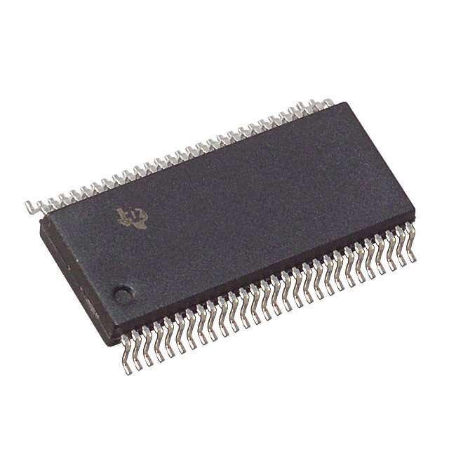
| 描述 | IC STROBED FIFO 512X18 56-SSOP先进先出 512 x 18 asynch 先进先出 Memory |
| 产品分类 | |
| FWFT支持 | 无 |
| 品牌 | Texas Instruments |
| 产品手册 | |
| 产品图片 |
|
| rohs | 符合RoHS无铅 / 符合限制有害物质指令(RoHS)规范要求 |
| 产品系列 | 内存,先进先出,Texas Instruments SN74ACT7804-40DL74ACT |
| 数据手册 | |
| 产品型号 | SN74ACT7804-40DL |
| 中继能力 | 无 |
| 产品种类 | 先进先出 |
| 供应商器件封装 | 56-SSOP |
| 其它名称 | 296-33664-5 |
| 功能 | 异步 |
| 包装 | 管件 |
| 单位重量 | 694.800 mg |
| 可编程标志支持 | 是 |
| 商标 | Texas Instruments |
| 存储容量 | 9K (512 x 18) |
| 安装类型 | 表面贴装 |
| 安装风格 | SMD/SMT |
| 定时类型 | Asynchronous |
| 封装 | Tube |
| 封装/外壳 | 56-BSSOP(0.295",7.50mm 宽) |
| 封装/箱体 | SSOP-56 |
| 工作温度 | 0°C ~ 70°C |
| 工厂包装数量 | 20 |
| 总线定向 | Unidirectional |
| 总线方向 | 单向 |
| 扩充类型 | 宽 |
| 数据总线宽度 | 18 bit |
| 数据速率 | 25MHz |
| 最大工作温度 | + 70 C |
| 最大工作电流 | 0.4 mA |
| 最小工作温度 | 0 C |
| 标准包装 | 20 |
| 电压-电源 | 4.5 V ~ 5.5 V |
| 电流-电源(最大值) | 400µA |
| 电源电压-最大 | 5.5 V |
| 电源电压-最小 | 4.5 V |
| 电路数量 | 2 |
| 系列 | SN74ACT7804 |
| 组织 | 512 k x 18 |
| 访问时间 | 20ns |


- 商务部:美国ITC正式对集成电路等产品启动337调查
- 曝三星4nm工艺存在良率问题 高通将骁龙8 Gen1或转产台积电
- 太阳诱电将投资9.5亿元在常州建新厂生产MLCC 预计2023年完工
- 英特尔发布欧洲新工厂建设计划 深化IDM 2.0 战略
- 台积电先进制程称霸业界 有大客户加持明年业绩稳了
- 达到5530亿美元!SIA预计今年全球半导体销售额将创下新高
- 英特尔拟将自动驾驶子公司Mobileye上市 估值或超500亿美元
- 三星加码芯片和SET,合并消费电子和移动部门,撤换高东真等 CEO
- 三星电子宣布重大人事变动 还合并消费电子和移动部门
- 海关总署:前11个月进口集成电路产品价值2.52万亿元 增长14.8%


PDF Datasheet 数据手册内容提取
SN74ACT7804 512 × 18 STROBED FIRST-IN, FIRST-OUT MEMORY SCAS204C – APRIL 1992 – REVISED APRIL 1998 (cid:1) Member of the Texas Instruments DL PACKAGE Widebus Family (TOP VIEW) (cid:1) Load Clock and Unload Clock Can Be RESET 1 56 OE Asynchronous or Coincident (cid:1) D17 2 55 Q17 512 Words by 18 Bits D16 3 54 Q16 (cid:1) Low-Power Advanced CMOS Technology D15 4 53 Q15 (cid:1) Full, Empty, and Half-Full Flags D14 5 52 GND (cid:1) Programmable Almost-Full/Almost-Empty D13 6 51 Q14 Flag D12 7 50 VCC (cid:1) D11 8 49 Q13 Fast Access Times of 15 ns With a 50-pF D10 9 48 Q12 Load and All Data Outputs Switching Simultaneously VCC 10 47 Q11 (cid:1) D9 11 46 Q10 Data Rates up to 50 MHz D8 12 45 Q9 (cid:1) 3-State Outputs GND 13 44 GND (cid:1) Pin-to-Pin Compatible With SN74ACT7806 D7 14 43 Q8 and SN74ACT7814 D6 15 42 Q7 (cid:1) Packaged in Shrink Small-Outline 300-mil D5 16 41 Q6 Package Using 25-mil Center-to-Center D4 17 40 Q5 Spacing D3 18 39 VCC D2 19 38 Q4 description D1 20 37 Q3 D0 21 36 Q2 A FIFO memory is a storage device that allows HF 22 35 GND data to be written into and read from its array at PEN 23 34 Q1 independent data rates. The SN74ACT7804 is a AF/AE 24 33 Q0 512-word by 18-bit FIFO for high speed and fast LDCK 25 32 UNCK access times. It processes data at rates up to NC 26 31 NC 50 MHz and access times of 15 ns in a bit-parallel NC 27 30 NC format. FULL 28 29 EMPTY Data is written into memory on a low-to-high transition at the load-clock (LDCK) input and is NC – No internal connection read out on a low-to-high transition at the unload-clock (UNCK) input. The memory is full when the number of words clocked in exceeds the number of words clocked out by 512. When the memory is full, LDCK signals have no effect on the data residing in memory. When the memory is empty, UNCK signals have no effect. Status of the FIFO memory is monitored by the full (FULL), empty (EMPTY), half-full (HF), and almost-full/almost-empty (AF/AE) flags. The FULL output is low when the memory is full and high when the memory is not full. The EMPTY output is low when the memory is empty and high when it is not empty. The HF output is high when the FIFO contains 256 or more words. The AF/AE status flag is a programmable flag. The first one or two low-to-high transitions of LDCK after reset are used to program the almost-empty offset value (X) and the almost-full offset value (Y) if program enable (PEN) is low. The AF/AE flag is high when the FIFO contains X or fewer words or (512 – Y) or more words. The AF/AE flag is low when the FIFO contains between (X + 1) and (511 – Y) words. Please be aware that an important notice concerning availability, standard warranty, and use in critical applications of TexasInstruments semiconductor products and disclaimers thereto appears at the end of this data sheet. Widebus is a trademark of Texas Instruments Incorporated. PRODUCTION DATA information is current as of publication date. Copyright 1998, Texas Instruments Incorporated Products conform to specifications per the terms of Texas Instruments standard warranty. Production processing does not necessarily include testing of all parameters. POST OFFICE BOX 655303 • DALLAS, TEXAS 75265 1
SN74ACT7804 512 × 18 STROBED FIRST-IN, FIRST-OUT MEMORY SCAS204C – APRIL 1992 – REVISED APRIL 1998 description (continued) A low level on the reset (RESET) input resets the internal stack pointers and sets FULL high, AF/AE high, HF low, and EMPTY low. The Q outputs are not reset to any specific logic level. The FIFO must be reset upon power up. The first word loaded into empty memory causes EMPTY to go high and the data to appear on the Q outputs. It is important to note that the first word does not have to be unloaded. The data outputs are noninverting with respect to the data inputs and are in the high-impedance state when the output-enable (OE) input is high. The SN74ACT7804 is characterized for operation from 0°C to 70°C. logic symbol† F FIFO 512 × 18 SN74ACT7804 1 RESET RESET 25 28 LDCK LDCK FULL FULL 22 32 HALF-FULL HF UNCK UNCK 24 56 ALMOST FULL/EMPTY AF/AE OE EN1 29 23 EMPTY EMPTY PEN PROGRAM ENABLE 21 33 D0 0 0 Q0 20 34 D1 Q1 19 36 D2 Q2 18 37 D3 Q3 17 38 D4 Q4 16 40 D5 Q5 15 41 D6 Q6 14 42 D7 Q7 12 43 D8 Q8 11 45 D9 Data Data 1 Q9 9 46 D10 Q10 8 47 D11 Q11 7 48 D12 Q12 6 49 D13 Q13 5 51 D14 Q14 4 53 D15 Q15 3 54 D16 Q16 2 55 D17 17 17 Q17 †This symbol is in accordance with ANSI/IEEE Std 91-1984 and IEC Publication 617-12. 2 POST OFFICE BOX 655303 • DALLAS, TEXAS 75265
SN74ACT7804 512 × 18 STROBED FIRST-IN, FIRST-OUT MEMORY SCAS204C – APRIL 1992 – REVISED APRIL 1998 functional block diagram OE D0–D17 Location 1 Read Location 2 UNCK Pointer 512 ×18 SRAM Write LDCK Pointer Location 511 Location 512 Q0–Q17 EMPTY Reset RESET Logic Status- FULL Flag Logic HF PEN AF/AE Terminal Functions TERMINAL II//OO DDEESSCCRRIIPPTTIIOONN NAME NO. Almost-full/almost-empty flag. Depth-offset values can be programmed for AF/AE, or the default value AF/AE 24 O of 64 can be used for both the almost-empty offset (X) and the almost-full offset (Y). AF/AE is high when memory contains X or fewer words or (512 – Y) or more words. AF/AE is high after reset. 2–9, 11–12, D0–D17 I 18-bit data input port 14–21 EMPTY 29 O Empty flag. EMPTY is low when the FIFO is empty. A FIFO reset also causes EMPTY to go low. FULL 28 O Full flag. FULL is low when the FIFO is full. A FIFO reset causes FULL to go high. HF 22 O Half-full flag. HF is high when the FIFO memory contains 256 or more words. HF is low after reset. LDCK 25 I Load clock. Data is written to the FIFO on the rising edge of LDCK when FULL is high. OE 56 I Output enable. When OE is high, the data outputs are in the high-impedance state. Program enable. After reset and before the first word is written to the FIFO, the binary value on D0–D7 PEN 23 I is latched as an AF/AE offset value when PEN is low and LDCK is high. 33–34, 36–38, Q0–Q17 40–43, 45–49, O 18-bit data output port 51, 53–55 RESET 1 I Reset. A low level on RESET resets the FIFO and drives AF/AE and FULL high and HF and EMPTY low. UNCK 32 I Unload clock. Data is read from the FIFO on the rising edge of UNCK when EMPTY is high. POST OFFICE BOX 655303 • DALLAS, TEXAS 75265 3
SN74ACT7804 512 × 18 STROBED FIRST-IN, FIRST-OUT MEMORY SCAS204C – APRIL 1992 – REVISED APRIL 1998 offset values for AF/AE The AF/AE flag has two programmable limits: the almost-empty offset value (X) and the almost-full offset value (Y). They can be programmed after the FIFO is reset and before the first word is written to memory. The AF/AE flag is high when the FIFO contains X or fewer words or (512 – Y) or more words. To program the offset values, PEN can be brought low after reset only when LDCK is low. On the following low-to-high transition of LDCK, the binary value on D0–D7 is stored as the almost-empty offset value (X) and the almost-full offset value (Y). Holding PEN low for another low-to-high transition of LDCK reprograms Y to the binary value on D0–D7 at the time of the second LDCK low-to-high transition. Writes to the FIFO memory are disabled while the offsets are programmed. A maximum value of 255 can be programmed for either X or Y (see Figure 1). To use the default values of X = Y = 64, PEN must be held high. RESET LDCK ÎÎÎÎÎÎÎÎÎÎ PEN Don’t Care ÎÎÎÎÎÎÎÎÎÎ ÏÏÏÏÏÏÏÏ D0–D7ÏÏÏDÏon’Ït CaÏre ÏÏ X and Y Y ÌÌÌÌÌ EMPTYÌÌÌÌÌ Figure 1. Programming X and Y Separately 4 POST OFFICE BOX 655303 • DALLAS, TEXAS 75265
RESET 1 PEN 0 LDCK Ï Ï Ï Ï Ï Ï Ï Ï Ï Ï Ï Ï Ï Ï Ï Ï Ï Ï Ï Ï Ï Ï Ï Ï Ï Ï Ï Ï Ï Ï Ï Ï D0–D17 W1 W2 (XW+1) W256 (51W2–Y) W512 Don’t Care Ï Ï Ï Ï Ï Ï Ï Ï Ï Ï Ï Ï Ï Ï Ï Ï Ï Ï Ï Ï Ï Ï Ï Ï Ï Ï Ï Ï Ï Ï Ï Ï PO UNCK S T O F FIC 1 E B 0 O OE X 5 6 1 55303 D• Q0–Q17 Ï Ï W1 W2 (YW+1) (YW+2) W257 W258 (51W2–X) (51W3–X) W511 W512 ÏÏ ÏÏ ÏÏ ÏÏ 2 1× A 8 LLA EMPTY Ï Ï S S, TE Ï Ï TR XA AF/AE O S 7 Ï Ï B 5 2 E 65 HF Ï Ï D ÏÏ ÏÏ F S IR FULL Ï Ï CA S S2 T 0 - 4 I C N Define the AF/AE Flag Using – AP , F the Default Value of X and Y RIL IR 1 S Figure 2. Write, Read, and Flag Timing Reference 99 T 2 - – OS R UN E V T7 IS 4 E MA D A EC PR MT IL O7 19 R80 5 98 Y4
SN74ACT7804 512 × 18 STROBED FIRST-IN, FIRST-OUT MEMORY SCAS204C – APRIL 1992 – REVISED APRIL 1998 absolute maximum ratings over operating free-air temperature range (unless otherwise noted)† Supply voltage range, V . . . . . . . . . . . . . . . . . . . . . . . . . . . . . . . . . . . . . . . . . . . . . . . . . . . . . . . . . . –0.5 V to 7 V CC Input voltage range, V . . . . . . . . . . . . . . . . . . . . . . . . . . . . . . . . . . . . . . . . . . . . . . . . . . . . . . . . . . . . . . –0.5 V to 7 V I Voltage range applied to a disabled 3-state output . . . . . . . . . . . . . . . . . . . . . . . . . . . . . . . . . . . . . –0.5 V to 5.5 V Package thermal impedance, q (see Note 1) . . . . . . . . . . . . . . . . . . . . . . . . . . . . . . . . . . . . . . . . . . . . . . 74°C/W JA Storage temperature range, T . . . . . . . . . . . . . . . . . . . . . . . . . . . . . . . . . . . . . . . . . . . . . . . . . . . –65°C to 150°C stg †Stresses beyond those listed under “absolute maximum ratings” may cause permanent damage to the device. These are stress ratings only, and functional operation of the device at these or any other conditions beyond those indicated under “recommended operating conditions” is not implied. Exposure to absolute-maximum-rated conditions for extended periods may affect device reliability. NOTE 1: The package thermal impedance is calculated in accordance with JESD 51. recommended operating conditions ’ACT7804-20 ’ACT7804-25 ’ACT7804-40 UUNNIITT MIN MAX MIN MAX MIN MAX VCC Supply voltage 4.5 5.5 4.5 5.5 4.5 5.5 V VIH High-level input voltage 2 2 2 V VIL Low-level input voltage 0.8 0.8 0.8 V IOH High-level output current Q outputs, flags –8 –8 –8 mA Q outputs 16 16 16 IIOOLL LLooww-lleevveell oouuttppuutt ccuurrrreenntt mmAA Flags 8 8 8 TA Operating free-air temperature 0 70 0 70 0 70 °C electrical characteristics over recommended operating free-air temperature range (unless otherwise noted) PARAMETER TEST CONDITIONS MIN TYP‡ MAX UNIT VOH VCC = 4.5 V, IOH = –8 mA 2.4 V Flags VCC = 4.5 V, IOL = 8 mA 0.5 VVOOLL VV Q outputs VCC = 4.5 V, IOL = 16 mA 0.5 II VCC = 5.5 V, VI = VCC or 0 ±5 m A IOZ VCC = 5.5 V, VO = VCC or 0 ±5 m A ICC VCC = 5.5 V, VI = VCC – 0.2 V or 0 400 m A D ICC§ VCC = 5.5 V, One input at 3.4 V, Other inputs at VCC or GND 1 mA Ci VI = 0, f = 1 MHz 4 pF Co VO = 0, f = 1 MHz 8 pF ‡All typical values are at VCC = 5 V, TA = 25°C. §This is the supply current for each input that is at one of the specified TTL voltage levels rather 0 V or VCC. 6 POST OFFICE BOX 655303 • DALLAS, TEXAS 75265
SN74ACT7804 512 × 18 STROBED FIRST-IN, FIRST-OUT MEMORY SCAS204C – APRIL 1992 – REVISED APRIL 1998 timing requirements over recommended operating conditions (see Figures 1 through 3) ’ACT7804-20 ’ACT7804-25 ’ACT7804-40 UUNNIITT MIN MAX MIN MAX MIN MAX fclock Clock frequency 50 40 25 MHz LDCK high or low 7 8 12 UNCK high or low 7 8 12 ttw PPuullssee dduurraattiioonn nnss PEN low 7 8 12 RESET low 10 10 12 D0–D17 before LDCK↑ 5 5 5 tsu Setup time PEN before LDCK↑ 5 5 5 ns LDCK inactive before RESET high 5 6 6 D0–D17 after LDCK↑ 0 0 0 LDCK inactive after RESET high 5 6 6 tthh HHoolldd ttiimmee nnss PEN low after LDCK↑ 3 3 3 PEN high after LDCK↓ 0 0 0 switching characteristics over recommended ranges of supply voltage and operating free-air temperature, C = 50 pF (unless otherwise noted) (see Figure 3) L FROM TO ’ACT7804-20 ’ACT7804-25 ’ACT7804-40 PPAARRAAMMEETTEERR UUNNIITT (INPUT) (OUTPUT) MIN TYP† MAX MIN MAX MIN MAX fmax LDCK or UNCK 50 40 25 MHz LDCK↑ 9 20 9 22 9 24 ttpdd AAnnyy QQ nnss UNCK↑ 6 11.5 15 6 18 6 20 tpd‡ UNCK↑ Any Q 10.5 ns tPLH LDCK↑ EMPTY 6 15 6 17 6 19 ns UNCK↑ 6 15 6 17 6 19 EEMMPPTTYY tPPHHLL RESET low 4 16 4 18 4 20 ns LDCK↑ FULL 6 15 6 17 6 19 UNCK↑ 6 15 6 17 6 19 ttPPLLHH FFUULLLL nnss RESET low 4 18 4 20 4 22 LDCK↑ 7 18 7 20 7 22 ttpdd AAFF//AAEE nnss UNCK↑ 7 18 7 20 7 22 RESET low AF/AE 2 10 2 12 2 14 ttPPLLHH nnss LDCK↑ HF 5 18 5 20 5 22 UNCK↑ 7 18 7 20 7 22 ttPPHHLL HHFF nnss RESET low 3 12 3 14 3 16 ten OE Any Q 2 9 2 10 2 11 ns tdis OE Any Q 2 10 2 11 2 12 ns †All typical values are at VCC = 5 V, TA = 25°C. ‡This parameter is measured at CL = 30 pF (see Figure 4). ° operating characteristics, V = 5 V, T = 25 CFigure 2 CC A PARAMETER TEST CONDITIONS TYP UNIT Cpd Power dissipation capacitance per FIFO channel Outputs enabled CL = 50 pF, f = 5 MHz 53 pF POST OFFICE BOX 655303 • DALLAS, TEXAS 75265 7
SN74ACT7804 512 × 18 STROBED FIRST-IN, FIRST-OUT MEMORY SCAS204C – APRIL 1992 – REVISED APRIL 1998 PARAMETER MEASUREMENT INFORMATION 7 V PARAMETER S1 S1 tPZH Open 500 W ten tPZL Closed From Output Test tPHZ Open Under Test Point tdis tPLZ Closed CL = 50 pF tPLH Open (see Note A) 500 W tpd tPHL Open LOAD CIRCUIT tw 3 V Input 1.5 V 1.5 V 3 V Timing 0 V 1.5 V Input 0 V VOLTAGE WAVEFORMS PULSE DURATION tsu th 3 V Data 3 V 1.5 V 1.5 V Input Output 0 V 1.5 V 1.5 V Control VOLTAGE WAVEFORMS 0 V SETUP AND HOLD TIMES tPZL tPLZ Output ≈3.5 V 3 V Input 1.5 V 1.5 V Waveform 1 1.5 V VOL + 0.3 V S1 at 7 V 0 V VOL tPLH tPHL tPZH tPHZ Output VOH VOH Waveform 2 1.5 V VOH – 0.3 V Output 1.5 V 1.5 V S1 at Open VOL ≈0 V VOLTAGE WAVEFORMS VOLTAGE WAVEFORMS PROPAGATION DELAY TIMES ENABLE AND DISABLE TIMES NOTE A: CL includes probe and jig capacitance. Figure 3. Load Circuit and Voltage Waveforms 8 POST OFFICE BOX 655303 • DALLAS, TEXAS 75265
SN74ACT7804 512 × 18 STROBED FIRST-IN, FIRST-OUT MEMORY SCAS204C – APRIL 1992 – REVISED APRIL 1998 TYPICAL CHARACTERISTICS PROPAGATION DELAY TIME SUPPLY CURRENT vs vs LOAD CAPACITANCE CLOCK FREQUENCY typ + 8 200 VCC = 5 V TA = 75°C TA = 25°C 180 CL = 0 pF ns typ + 6 RL = 500 W 160 VCC = 5.5 V e – mA VCC = 5 V m 140 ay Ti typ + 4 ent – 120 Del urr ation pply C 100 VCC = 4.5 V g typ + 2 u 80 a S op – – Pr CC(f) 60 pd typ I 40 t 20 typ – 2 0 0 50 100 150 200 250 300 0 10 20 30 40 50 60 70 CL – Load Capacitance – pF fclock – Clock Frequency – MHz Figure 4 Figure 5 POST OFFICE BOX 655303 • DALLAS, TEXAS 75265 9
SN74ACT7804 512 × 18 STROBED FIRST-IN, FIRST-OUT MEMORY SCAS204C – APRIL 1992 – REVISED APRIL 1998 APPLICATION INFORMATION SN74ACT7804 LDCK LDCK UNCK UNCK FULL EMPTY FULL EMPTY OE OE D18–D35 D0–D17 Q0–Q17 Q18–Q35 SN74ACT7804 LDCK UNCK FULL EMPTY OE D0–D17 D0–D17 Q0–Q17 Q0–Q17 Figure 6. Word-Width Expansion: 512 × 36 Bits 10 POST OFFICE BOX 655303 • DALLAS, TEXAS 75265
IMPORTANT NOTICE Texas Instruments and its subsidiaries (TI) reserve the right to make changes to their products or to discontinue any product or service without notice, and advise customers to obtain the latest version of relevant information to verify, before placing orders, that information being relied on is current and complete. All products are sold subject to the terms and conditions of sale supplied at the time of order acknowledgement, including those pertaining to warranty, patent infringement, and limitation of liability. TI warrants performance of its semiconductor products to the specifications applicable at the time of sale in accordance with TI’s standard warranty. Testing and other quality control techniques are utilized to the extent TI deems necessary to support this warranty. Specific testing of all parameters of each device is not necessarily performed, except those mandated by government requirements. CERTAIN APPLICATIONS USING SEMICONDUCTOR PRODUCTS MAY INVOLVE POTENTIAL RISKS OF DEATH, PERSONAL INJURY, OR SEVERE PROPERTY OR ENVIRONMENTAL DAMAGE (“CRITICAL APPLICATIONS”). TI SEMICONDUCTOR PRODUCTS ARE NOT DESIGNED, AUTHORIZED, OR WARRANTED TO BE SUITABLE FOR USE IN LIFE-SUPPORT DEVICES OR SYSTEMS OR OTHER CRITICAL APPLICATIONS. INCLUSION OF TI PRODUCTS IN SUCH APPLICATIONS IS UNDERSTOOD TO BE FULLY AT THE CUSTOMER’S RISK. In order to minimize risks associated with the customer’s applications, adequate design and operating safeguards must be provided by the customer to minimize inherent or procedural hazards. TI assumes no liability for applications assistance or customer product design. TI does not warrant or represent that any license, either express or implied, is granted under any patent right, copyright, mask work right, or other intellectual property right of TI covering or relating to any combination, machine, or process in which such semiconductor products or services might be or are used. TI’s publication of information regarding any third party’s products or services does not constitute TI’s approval, warranty or endorsement thereof. Copyright 1999, Texas Instruments Incorporated