ICGOO在线商城 > 集成电路(IC) > 逻辑 - 缓冲器,驱动器,接收器,收发器 > SN74ABT16952DLR
 Datasheet下载
- 型号: SN74ABT16952DLR
- 制造商: Texas Instruments
- 库位|库存: xxxx|xxxx
- 要求:
| 数量阶梯 | 香港交货 | 国内含税 |
| +xxxx | $xxxx | ¥xxxx |
查看当月历史价格
查看今年历史价格
SN74ABT16952DLR产品简介:
ICGOO电子元器件商城为您提供SN74ABT16952DLR由Texas Instruments设计生产,在icgoo商城现货销售,并且可以通过原厂、代理商等渠道进行代购。 SN74ABT16952DLR价格参考。Texas InstrumentsSN74ABT16952DLR封装/规格:逻辑 - 缓冲器,驱动器,接收器,收发器, Transceiver, Non-Inverting 2 Element 8 Bit per Element 3-State Output 56-SSOP。您可以下载SN74ABT16952DLR参考资料、Datasheet数据手册功能说明书,资料中有SN74ABT16952DLR 详细功能的应用电路图电压和使用方法及教程。
| 参数 | 数值 |
| 产品目录 | 集成电路 (IC) |
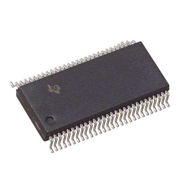
| 描述 | IC REGISTERED TRANSCVR 56SSOP |
| 产品分类 | |
| 品牌 | Texas Instruments |
| 数据手册 | |
| 产品图片 |
|
| 产品型号 | SN74ABT16952DLR |
| rohs | 无铅 / 符合限制有害物质指令(RoHS)规范要求 |
| 产品系列 | 74ABT |
| 供应商器件封装 | 56-SSOP |
| 元件数 | 2 |
| 其它名称 | 296-3936-1 |
| 包装 | 剪切带 (CT) |
| 安装类型 | 表面贴装 |
| 封装/外壳 | 56-BSSOP(0.295",7.50mm 宽) |
| 工作温度 | -40°C ~ 85°C |
| 标准包装 | 1 |
| 每元件位数 | 8 |
| 电压-电源 | 4.5 V ~ 5.5 V |
| 电流-输出高,低 | 32mA,64mA |
| 逻辑类型 | 寄存收发器,非反相 |


- 商务部:美国ITC正式对集成电路等产品启动337调查
- 曝三星4nm工艺存在良率问题 高通将骁龙8 Gen1或转产台积电
- 太阳诱电将投资9.5亿元在常州建新厂生产MLCC 预计2023年完工
- 英特尔发布欧洲新工厂建设计划 深化IDM 2.0 战略
- 台积电先进制程称霸业界 有大客户加持明年业绩稳了
- 达到5530亿美元!SIA预计今年全球半导体销售额将创下新高
- 英特尔拟将自动驾驶子公司Mobileye上市 估值或超500亿美元
- 三星加码芯片和SET,合并消费电子和移动部门,撤换高东真等 CEO
- 三星电子宣布重大人事变动 还合并消费电子和移动部门
- 海关总署:前11个月进口集成电路产品价值2.52万亿元 增长14.8%


PDF Datasheet 数据手册内容提取
SN54ABT16952, SN74ABT16952 16-BIT REGISTERED TRANSCEIVERS WITH 3-STATE OUTPUTS SCBS082C – FEBRUARY 1991 – REVISED JANUARY 1997 (cid:1) Members of the Texas Instruments SN54ABT16952...WD PACKAGE WidebusE Family SN74ABT16952...DGG OR DL PACKAGE (cid:1) (TOP VIEW) State-of-the-Art EPIC-II B BiCMOS Design Significantly Reduces Power Dissipation 1OEAB 1 56 1OEBA (cid:1) Latch-Up Performance Exceeds 500 mA Per 1CLKAB 2 55 1CLKBA JEDEC Standard JESD-17 1CLKENAB 3 54 1CLKENBA (cid:1) Typical VOLP (Output Ground Bounce) < 1 V GND 4 53 GND at VCC = 5 V, TA = 25°C 1A1 5 52 1B1 (cid:1) Distributed V and GND Pin Configuration 1A2 6 1B2 CC Minimizes High-Speed Switching Noise VCC 7 50 VCC (cid:1) 1A3 8 49 1B3 Flow-Through Architecture Optimizes PCB 1A4 9 48 1B4 Layout (cid:1) 1A5 10 47 1B5 High-Drive Outputs (–32-mA I , 64-mA I ) OH OL GND 11 46 GND (cid:1) Package Options Include Plastic 300-mil 1A6 12 45 1B6 Shrink Small-Outline (DL) and Thin Shrink 1A7 13 44 1B7 Small-Outline (DGG) Packages and 380-mil 1A8 14 43 1B8 Fine-Pitch Ceramic Flat (WD) Package 2A1 15 42 2B1 Using 25-mil Center-to-Center Spacings 2A2 16 41 2B2 2A3 17 40 2B3 description GND 18 39 GND The ’ABT16952 are 16-bit registered transceivers 2A4 19 38 2B4 that contain two sets of D-type flip-flops for 2A5 20 37 2B5 temporary storage of data flowing in either 2A6 21 36 2B6 direction. The ’ABT16952 can be used as two 8-bit VCC 22 35 VCC transceivers or one 16-bit transceiver. Data on the 2A7 23 34 2B7 A or B bus is stored in the registers on the 2A8 24 33 2B8 low-to-high transition of the clock (CLKAB or GND 25 32 GND CLKBA) input provided that the clock-enable 2CLKENAB 26 31 2CLKENBA (CLKENAB or CLKENBA) input is low. Taking the 2CLKAB 27 30 2CLKBA output-enable (OEAB or OEBA) input low 2OEAB 28 29 2OEBA accesses the data on either port. To ensure the high-impedance state during power up or power down, OE should be tied to V through a pullup CC resistor; the minimum value of the resistor is determined by the current-sinking capability of the driver. The SN54ABT16952 is characterized for operation over the full military temperature range of –55°C to 125°C. The SN74ABT16952 is characterized for operation from –40°C to 85°C. Please be aware that an important notice concerning availability, standard warranty, and use in critical applications of TexasInstruments semiconductor products and disclaimers thereto appears at the end of this data sheet. Widebus and EPIC-II B are trademarks of Texas Instruments Incorporated. UNLESS OTHERWISE NOTED this document contains PRODUCTION Copyright 1997, Texas Instruments Incorporated DATA information current as of publication date. Products conform to specifications per the terms of Texas Instruments standard warranty. Production processing does not necessarily include testing of all parameters. POST OFFICE BOX 655303 • DALLAS, TEXAS 75265 1
SN54ABT16952, SN74ABT16952 16-BIT REGISTERED TRANSCEIVERS WITH 3-STATE OUTPUTS SCBS082C – FEBRUARY 1991 – REVISED JANUARY 1997 FUNCTION TABLE† INPUTS OUTPUT CLKENAB CLKAB OEAB A B H X L X B0‡ X L L X B0‡ L ↑ L L L L ↑ L H H X X H X Z †A-to-B data flow is shown; B-to-A data flow is similar, but uses CLKENBA, CLKBA, and OEBA. ‡Level of B before the indicated steady-state input conditions were established 2 POST OFFICE BOX 655303 • DALLAS, TEXAS 75265
SN54ABT16952, SN74ABT16952 16-BIT REGISTERED TRANSCEIVERS WITH 3-STATE OUTPUTS SCBS082C – FEBRUARY 1991 – REVISED JANUARY 1997 logic symbol† 56 1OEBA EN3 54 1CLKENBA G1 55 1CLKBA 1C5 1 1OEAB EN4 3 1CLKENAB G2 2 1CLKAB 2C6 29 2OEBA EN9 31 2CLKENBA G7 30 2CLKBA 7C11 28 2OEAB EN10 26 2CLKENAB G8 27 2CLKAB 8C12 5 52 1A1 3 5D 1B1 6D 4 6 51 1A2 1B2 8 49 1A3 1B3 9 48 1A4 1B4 10 47 1A5 1B5 12 45 1A6 1B6 13 44 1A7 1B7 14 43 1A8 1B8 15 42 2A1 9 11D 2B1 12D 10 16 41 2A2 2B2 17 40 2A3 2B3 19 38 2A4 2B4 20 37 2A5 2B5 21 36 2A6 2B6 23 34 2A7 2B7 24 33 2A8 2B8 †This symbol is in accordance with ANSI/IEEE Std 91-1984 and IEC Publication 617-12. POST OFFICE BOX 655303 • DALLAS, TEXAS 75265 3
SN54ABT16952, SN74ABT16952 16-BIT REGISTERED TRANSCEIVERS WITH 3-STATE OUTPUTS SCBS082C – FEBRUARY 1991 – REVISED JANUARY 1997 logic diagram (positive logic) 3 54 1CLKENAB 1CLKENBA 2 55 1CLKAB 1CLKBA 56 1 1OEBA 1OEAB One of Eight C1 Channels CE 5 52 1A1 1D 1B1 C1 CE 1D To Seven Other Channels 26 31 2CLKENAB 2CLKENBA 27 30 2CLKAB 2CLKBA 29 28 2OEBA 2OEAB One of Eight C1 Channels 15 CE 42 2A1 1D 2B1 C1 CE 1D To Seven Other Channels 4 POST OFFICE BOX 655303 • DALLAS, TEXAS 75265
SN54ABT16952, SN74ABT16952 16-BIT REGISTERED TRANSCEIVERS WITH 3-STATE OUTPUTS SCBS082C – FEBRUARY 1991 – REVISED JANUARY 1997 absolute maximum ratings over operating free-air temperature range (unless otherwise noted)† Supply voltage range, V . . . . . . . . . . . . . . . . . . . . . . . . . . . . . . . . . . . . . . . . . . . . . . . . . . . . . . . . . . –0.5 V to 7 V CC Input voltage range, V (except I/O ports) (see Note 1) . . . . . . . . . . . . . . . . . . . . . . . . . . . . . . . . . . –0.5 V to 7 V I Voltage range applied to any output in the high or power-off state, V . . . . . . . . . . . . . . . . . . . . –0.5 V to 5.5 V O Current into any output in the low state, I : SN54ABT16952 . . . . . . . . . . . . . . . . . . . . . . . . . . . . . . . . . . 96 mA O SN74ABT16952 . . . . . . . . . . . . . . . . . . . . . . . . . . . . . . . . . 128 mA Input clamp current, IIK (VI < 0) . . . . . . . . . . . . . . . . . . . . . . . . . . . . . . . . . . . . . . . . . . . . . . . . . . . . . . . . . . . . –18 mA Output clamp current, IOK (VO < 0) . . . . . . . . . . . . . . . . . . . . . . . . . . . . . . . . . . . . . . . . . . . . . . . . . . . . . . . . –50 mA Package thermal impedance, q (see Note 2): DGG package . . . . . . . . . . . . . . . . . . . . . . . . . . . . . . . . 81°C/W JA DL package . . . . . . . . . . . . . . . . . . . . . . . . . . . . . . . . . . 74°C/W Storage temperature range, T . . . . . . . . . . . . . . . . . . . . . . . . . . . . . . . . . . . . . . . . . . . . . . . . . . . . –65°C to 150°C stg †Stresses beyond those listed under “absolute maximum ratings” may cause permanent damage to the device. These are stress ratings only, and functional operation of the device at these or any other conditions beyond those indicated under “recommended operating conditions” is not implied. Exposure to absolute-maximum-rated conditions for extended periods may affect device reliability. NOTES: 1. The input and output negative-voltage ratings may be exceeded if the input and output clamp-current ratings are observed. 2. The package thermal impedance is calculated in accordance with EIA/JEDEC Std JESD51. recommended operating conditions (see Note 3) SN54ABT16952 SN74ABT16952 UUNNIITT MIN MAX MIN MAX VCC Supply voltage 4.5 5.5 4.5 5.5 V VIH High-level input voltage 2 2 V VIL Low-level input voltage 0.8 0.8 V VI Input voltage 0 VCC 0 VCC V IOH High-level output current –24 –32 mA IOL Low-level output current 48 64 mA D t/D v Input transition rise or fall rate Outputs enabled 10 10 ns/V TA Operating free-air temperature –55 125 –40 85 °C NOTE 3: Unused pins (input or I/O) must be held high or low to prevent them from floating. PRODUCT PREVIEW information concerns products in the formative or design phase of development. Characteristic data and other specifications are design goals. Texas Instruments reserves the right to change or discontinue these products without notice. POST OFFICE BOX 655303 • DALLAS, TEXAS 75265 5
SN54ABT16952, SN74ABT16952 16-BIT REGISTERED TRANSCEIVERS WITH 3-STATE OUTPUTS SCBS082C – FEBRUARY 1991 – REVISED JANUARY 1997 electrical characteristics over recommended operating free-air temperature range (unless otherwise noted) TA = 25°C SN54ABT16952 SN74ABT16952 PPAARRAAMMEETTEERR TTEESSTT CCOONNDDIITTIIOONNSS UUNNIITT MIN TYP† MAX MIN MAX MIN MAX VIK VCC = 4.5 V, II = –18 mA –1.2 –1.2 –1.2 V VCC = 4.5 V, IOH = –3 mA 2.5 2.5 2.5 VCC = 5 V, IOH = –3 mA 3 3 3 VVOOHH VV IOH = –24 mA 2 2 VVCCCC == 44.55 VV IOH = –32 mA 2* 2 IOL = 48 mA 0.55 0.55 VVOOLL VVCCCC == 44.55 VV VV IOL = 64 mA 0.55* 0.55 Vhys 100 mV Control inputs ±1 ±1 ±1 IIII VVCCCC == 55.55 VV, VVII == VVCCCC oorr GGNNDD mm AA A or B ports ±100 ±100 ±100 IOZH‡ VCC = 5.5 V, VO = 2.7 V 50 50 50 m A IOZL‡ VCC = 5.5 V, VO = 0.5 V –50 –50 –50 m A Ioff VCC = 0, VI or VO ≤ 4.5 V ±100 ±100 m A ICEX VVCOC = =5 .55. 5V V, Outputs high 50 50 50 m A IO§ VCC = 5.5 V, VO = 2.5 V –50 –100 –200 –50 –200 –50 –200 mA Outputs high 2 2 2 VVCCCC == 55..55 VV,, ICC A or B ports IO = 0, Outputs low 35 35 35 mA VI = VCC or GND Outputs disabled 2 2 2 D ICC¶ VOCthCe r= i n5p.5u tVs ,a Ot nVeC iCn pourt GaNt 3D.4 V, 0.5 0.5 0.5 mA Ci Control inputs VI = 2.5 V or 0.5 V 3 pF Cio A or B ports VO = 2.5 V or 0.5 V 8.5 pF * On products compliant to MIL-PRF-38535, this parameter does not apply. †All typical values are at VCC = 5 V. ‡The parameters IOZH and IOZL include the input leakage current. §Not more than one output should be tested at a time, and the duration of the test should not exceed one second. ¶This is the increase in supply current for each input that is at the specified TTL voltage level rather than VCC or GND. PRODUCT PREVIEW information concerns products in the formative or design phase of development. Characteristic data and other specifications are design goals. Texas Instruments reserves the right to change or discontinue these products without notice. 6 POST OFFICE BOX 655303 • DALLAS, TEXAS 75265
SN54ABT16952, SN74ABT16952 16-BIT REGISTERED TRANSCEIVERS WITH 3-STATE OUTPUTS SCBS082C – FEBRUARY 1991 – REVISED JANUARY 1997 timing requirements over recommended ranges of supply voltage and operating free-air temperature (unless otherwise noted) (see Figure 1) VCC = 5 V, SN54ABT16952 SN74ABT16952 TA = 25°C UNIT MIN MAX MIN MAX MIN MAX fclock Clock frequency 0 150 0 150 0 150 MHz tw† Pulse duration, CLKAB or CLKBA high or low 3.3 3.3 3.3 ns Setup time,, A or B 3.5 3.5 3.5 ttsu before CLKAB↑ or CLKBA↑ CLKENAB or CLKENBA 3 3 3 nnss Hold time,, A or B 1 1 1 tthh after CLKAB↑ or CLKBA↑ CLKENAB or CLKENBA 1 1 1 nnss †This parameter is warranted, but not production tested. switching characteristics over recommended ranges of supply voltage and operating free-air temperature, C = 50 pF (unless otherwise noted) (see Figure 1) L VCC = 5 V, PARAMETER FROM TO TA = 25°C SN54ABT16952 SN74ABT16952 UNIT ((IINNPPUUTT)) ((OOUUTTPPUUTT)) MIN TYP MAX MIN MAX MIN MAX fmax 150 150 150 MHz tPLH 1 2.6 3.9 1 4.4 1 4.3 CCLLKK AA oorr BB nnss tPHL 1 2.6 4.2 1 4.6 1 4.5 tPZH 1 2.5 3.8 1 4.7 1 4.6 OOEE AA oorr BB nnss tPZL 1 2.8 5.1 1 6.1 1 6 tPHZ 1.7 3.4 4.7 1.7 6.1 1.7 5.5 OOEE AA oorr BB nnss tPLZ 1.3 3 3.9 1.3 4.8 1.3 4.2 PRODUCT PREVIEW information concerns products in the formative or design phase of development. Characteristic data and other specifications are design goals. Texas Instruments reserves the right to change or discontinue these products without notice. POST OFFICE BOX 655303 • DALLAS, TEXAS 75265 7
SN54ABT16952, SN74ABT16952 16-BIT REGISTERED TRANSCEIVERS WITH 3-STATE OUTPUTS SCBS082C – FEBRUARY 1991 – REVISED JANUARY 1997 PARAMETER MEASUREMENT INFORMATION 7 V TEST S1 500 W S1 Open From Output tPLH/tPHL Open Under Test GND tPLZ/tPZL 7 V CL = 50 pF 500 W tPHZ/tPZH Open (see Note A) 3 V LOAD CIRCUIT Timing Input 1.5 V 0 V tw tsu th 3 V 3 V Input 1.5 V 1.5 V Data Input 1.5 V 1.5 V 0 V 0 V VOLTAGE WAVEFORMS VOLTAGE WAVEFORMS PULSE DURATION SETUP AND HOLD TIMES 3 V 3 V OOuuttppuutt Input 1.5 V 1.5 V 1.5 V 1.5 V CCoonnttrrooll 0 V 0 V tPZL tPLH tPHL VOH Output tPLZ 3.5 V Output 1.5 V 1.5 V VOL WavSe1f oatr m7 V1 1.5 V VOL + 0.3 V VOL (see Note B) tPHZ tPHL tPLH tPZH Output VOH VOH Output 1.5 V 1.5 V WSa1v aetf oOrpme n2 1.5 V VOH – 0.3 V VOL (see Note B) ≈ 0 V VOLTAGE WAVEFORMS VOLTAGE WAVEFORMS PROPAGATION DELAY TIMES ENABLE AND DISABLE TIMES INVERTING AND NONINVERTING OUTPUTS LOW- AND HIGH-LEVEL ENABLING NOTES: A. CL includes probe and jig capacitance. B. Waveform 1 is for an output with internal conditions such that the output is low except when disabled by the output control. Waveform2 is for an output with internal conditions such that the output is high except when disabled by the output control. C. All input pulses are supplied by generators having the following characteristics: PRR ≤ 10 MHz, ZO = 50 W , tr ≤ 2.5 ns, tf≤ 2.5 ns. D. The outputs are measured one at a time with one transition per measurement. Figure 1. Load Circuit and Voltage Waveforms 8 POST OFFICE BOX 655303 • DALLAS, TEXAS 75265
PACKAGE OPTION ADDENDUM www.ti.com 18-Sep-2008 PACKAGING INFORMATION OrderableDevice Status(1) Package Package Pins Package EcoPlan(2) Lead/BallFinish MSLPeakTemp(3) Type Drawing Qty 74ABT16952DGGRE4 ACTIVE TSSOP DGG 56 2000 Green(RoHS& CUNIPDAU Level-1-260C-UNLIM noSb/Br) 74ABT16952DGGRG4 ACTIVE TSSOP DGG 56 2000 Green(RoHS& CUNIPDAU Level-1-260C-UNLIM noSb/Br) SN74ABT16952DGGR ACTIVE TSSOP DGG 56 2000 Green(RoHS& CUNIPDAU Level-1-260C-UNLIM noSb/Br) SN74ABT16952DL ACTIVE SSOP DL 56 20 Green(RoHS& CUNIPDAU Level-1-260C-UNLIM noSb/Br) SN74ABT16952DLG4 ACTIVE SSOP DL 56 20 Green(RoHS& CUNIPDAU Level-1-260C-UNLIM noSb/Br) SN74ABT16952DLR ACTIVE SSOP DL 56 1000 Green(RoHS& CUNIPDAU Level-1-260C-UNLIM noSb/Br) SN74ABT16952DLRG4 ACTIVE SSOP DL 56 1000 Green(RoHS& CUNIPDAU Level-1-260C-UNLIM noSb/Br) (1)Themarketingstatusvaluesaredefinedasfollows: ACTIVE:Productdevicerecommendedfornewdesigns. LIFEBUY:TIhasannouncedthatthedevicewillbediscontinued,andalifetime-buyperiodisineffect. NRND:Notrecommendedfornewdesigns.Deviceisinproductiontosupportexistingcustomers,butTIdoesnotrecommendusingthispartin anewdesign. PREVIEW:Devicehasbeenannouncedbutisnotinproduction.Samplesmayormaynotbeavailable. OBSOLETE:TIhasdiscontinuedtheproductionofthedevice. (2)EcoPlan-Theplannedeco-friendlyclassification:Pb-Free(RoHS),Pb-Free(RoHSExempt),orGreen(RoHS&noSb/Br)-pleasecheck http://www.ti.com/productcontentforthelatestavailabilityinformationandadditionalproductcontentdetails. TBD:ThePb-Free/Greenconversionplanhasnotbeendefined. Pb-Free(RoHS):TI'sterms"Lead-Free"or"Pb-Free"meansemiconductorproductsthatarecompatiblewiththecurrentRoHSrequirements forall6substances,includingtherequirementthatleadnotexceed0.1%byweightinhomogeneousmaterials.Wheredesignedtobesoldered athightemperatures,TIPb-Freeproductsaresuitableforuseinspecifiedlead-freeprocesses. Pb-Free(RoHSExempt):ThiscomponenthasaRoHSexemptionforeither1)lead-basedflip-chipsolderbumpsusedbetweenthedieand package, or 2) lead-based die adhesive used between the die and leadframe. The component is otherwise considered Pb-Free (RoHS compatible)asdefinedabove. Green(RoHS&noSb/Br):TIdefines"Green"tomeanPb-Free(RoHScompatible),andfreeofBromine(Br)andAntimony(Sb)basedflame retardants(BrorSbdonotexceed0.1%byweightinhomogeneousmaterial) (3) MSL, Peak Temp. -- The Moisture Sensitivity Level rating according to the JEDEC industry standard classifications, and peak solder temperature. Important Information and Disclaimer:The information provided on this page represents TI's knowledge and belief as of the date that it is provided. TI bases its knowledge and belief on information provided by third parties, and makes no representation or warranty as to the accuracy of such information. Efforts are underway to better integrate information from third parties. TI has taken and continues to take reasonable steps to provide representative and accurate information but may not have conducted destructive testing or chemical analysis on incomingmaterialsandchemicals.TIandTIsuppliersconsidercertaininformationtobeproprietary,andthusCASnumbersandotherlimited informationmaynotbeavailableforrelease. InnoeventshallTI'sliabilityarisingoutofsuchinformationexceedthetotalpurchasepriceoftheTIpart(s)atissueinthisdocumentsoldbyTI toCustomeronanannualbasis. Addendum-Page1
PACKAGE MATERIALS INFORMATION www.ti.com 11-Mar-2008 TAPE AND REEL INFORMATION *Alldimensionsarenominal Device Package Package Pins SPQ Reel Reel A0(mm) B0(mm) K0(mm) P1 W Pin1 Type Drawing Diameter Width (mm) (mm) Quadrant (mm) W1(mm) SN74ABT16952DGGR TSSOP DGG 56 2000 330.0 24.4 8.6 15.6 1.8 12.0 24.0 Q1 SN74ABT16952DLR SSOP DL 56 1000 330.0 32.4 11.35 18.67 3.1 16.0 32.0 Q1 PackMaterials-Page1
PACKAGE MATERIALS INFORMATION www.ti.com 11-Mar-2008 *Alldimensionsarenominal Device PackageType PackageDrawing Pins SPQ Length(mm) Width(mm) Height(mm) SN74ABT16952DGGR TSSOP DGG 56 2000 346.0 346.0 41.0 SN74ABT16952DLR SSOP DL 56 1000 346.0 346.0 49.0 PackMaterials-Page2
IMPORTANTNOTICE TexasInstrumentsIncorporatedanditssubsidiaries(TI)reservetherighttomakecorrections,modifications,enhancements,improvements, andotherchangestoitsproductsandservicesatanytimeandtodiscontinueanyproductorservicewithoutnotice.Customersshould obtainthelatestrelevantinformationbeforeplacingordersandshouldverifythatsuchinformationiscurrentandcomplete.Allproductsare soldsubjecttoTI’stermsandconditionsofsalesuppliedatthetimeoforderacknowledgment. TIwarrantsperformanceofitshardwareproductstothespecificationsapplicableatthetimeofsaleinaccordancewithTI’sstandard warranty.TestingandotherqualitycontroltechniquesareusedtotheextentTIdeemsnecessarytosupportthiswarranty.Exceptwhere mandatedbygovernmentrequirements,testingofallparametersofeachproductisnotnecessarilyperformed. TIassumesnoliabilityforapplicationsassistanceorcustomerproductdesign.Customersareresponsiblefortheirproductsand applicationsusingTIcomponents.Tominimizetherisksassociatedwithcustomerproductsandapplications,customersshouldprovide adequatedesignandoperatingsafeguards. TIdoesnotwarrantorrepresentthatanylicense,eitherexpressorimplied,isgrantedunderanyTIpatentright,copyright,maskworkright, orotherTIintellectualpropertyrightrelatingtoanycombination,machine,orprocessinwhichTIproductsorservicesareused.Information publishedbyTIregardingthird-partyproductsorservicesdoesnotconstitutealicensefromTItousesuchproductsorservicesora warrantyorendorsementthereof.Useofsuchinformationmayrequirealicensefromathirdpartyunderthepatentsorotherintellectual propertyofthethirdparty,oralicensefromTIunderthepatentsorotherintellectualpropertyofTI. ReproductionofTIinformationinTIdatabooksordatasheetsispermissibleonlyifreproductioniswithoutalterationandisaccompanied byallassociatedwarranties,conditions,limitations,andnotices.Reproductionofthisinformationwithalterationisanunfairanddeceptive businesspractice.TIisnotresponsibleorliableforsuchaltereddocumentation.Informationofthirdpartiesmaybesubjecttoadditional restrictions. ResaleofTIproductsorserviceswithstatementsdifferentfromorbeyondtheparametersstatedbyTIforthatproductorservicevoidsall expressandanyimpliedwarrantiesfortheassociatedTIproductorserviceandisanunfairanddeceptivebusinesspractice.TIisnot responsibleorliableforanysuchstatements. TIproductsarenotauthorizedforuseinsafety-criticalapplications(suchaslifesupport)whereafailureoftheTIproductwouldreasonably beexpectedtocauseseverepersonalinjuryordeath,unlessofficersofthepartieshaveexecutedanagreementspecificallygoverning suchuse.Buyersrepresentthattheyhaveallnecessaryexpertiseinthesafetyandregulatoryramificationsoftheirapplications,and acknowledgeandagreethattheyaresolelyresponsibleforalllegal,regulatoryandsafety-relatedrequirementsconcerningtheirproducts andanyuseofTIproductsinsuchsafety-criticalapplications,notwithstandinganyapplications-relatedinformationorsupportthatmaybe providedbyTI.Further,BuyersmustfullyindemnifyTIanditsrepresentativesagainstanydamagesarisingoutoftheuseofTIproductsin suchsafety-criticalapplications. TIproductsareneitherdesignednorintendedforuseinmilitary/aerospaceapplicationsorenvironmentsunlesstheTIproductsare specificallydesignatedbyTIasmilitary-gradeor"enhancedplastic."OnlyproductsdesignatedbyTIasmilitary-grademeetmilitary specifications.BuyersacknowledgeandagreethatanysuchuseofTIproductswhichTIhasnotdesignatedasmilitary-gradeissolelyat theBuyer'srisk,andthattheyaresolelyresponsibleforcompliancewithalllegalandregulatoryrequirementsinconnectionwithsuchuse. TIproductsareneitherdesignednorintendedforuseinautomotiveapplicationsorenvironmentsunlessthespecificTIproductsare designatedbyTIascompliantwithISO/TS16949requirements.Buyersacknowledgeandagreethat,iftheyuseanynon-designated productsinautomotiveapplications,TIwillnotberesponsibleforanyfailuretomeetsuchrequirements. FollowingareURLswhereyoucanobtaininformationonotherTexasInstrumentsproductsandapplicationsolutions: Products Applications Amplifiers amplifier.ti.com Audio www.ti.com/audio DataConverters dataconverter.ti.com Automotive www.ti.com/automotive DSP dsp.ti.com Broadband www.ti.com/broadband ClocksandTimers www.ti.com/clocks DigitalControl www.ti.com/digitalcontrol Interface interface.ti.com Medical www.ti.com/medical Logic logic.ti.com Military www.ti.com/military PowerMgmt power.ti.com OpticalNetworking www.ti.com/opticalnetwork Microcontrollers microcontroller.ti.com Security www.ti.com/security RFID www.ti-rfid.com Telephony www.ti.com/telephony RF/IFandZigBee®Solutions www.ti.com/lprf Video&Imaging www.ti.com/video Wireless www.ti.com/wireless MailingAddress:TexasInstruments,PostOfficeBox655303,Dallas,Texas75265 Copyright©2008,TexasInstrumentsIncorporated