ICGOO在线商城 > 集成电路(IC) > 逻辑 - 栅极和逆变器 > SN7414N
 Datasheet下载
- 型号: SN7414N
- 制造商: Texas Instruments
- 库位|库存: xxxx|xxxx
- 要求:
| 数量阶梯 | 香港交货 | 国内含税 |
| +xxxx | $xxxx | ¥xxxx |
查看当月历史价格
查看今年历史价格
SN7414N产品简介:
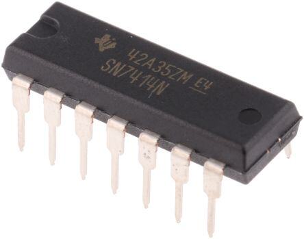
ICGOO电子元器件商城为您提供SN7414N由Texas Instruments设计生产,在icgoo商城现货销售,并且可以通过原厂、代理商等渠道进行代购。 SN7414N价格参考¥6.91-¥15.55。Texas InstrumentsSN7414N封装/规格:逻辑 - 栅极和逆变器, Inverter IC 6 Channel Schmitt Trigger 14-PDIP。您可以下载SN7414N参考资料、Datasheet数据手册功能说明书,资料中有SN7414N 详细功能的应用电路图电压和使用方法及教程。
| 参数 | 数值 |
| 产品目录 | 集成电路 (IC)半导体 |
| 描述 | IC HEX SCHMITT-TRIG INV 14-DIP变换器 Hex Schmitt-Trigger 变换器 |
| 产品分类 | |
| 品牌 | Texas Instruments |
| 产品手册 | |
| 产品图片 |
|
| rohs | 符合RoHS无铅 / 符合限制有害物质指令(RoHS)规范要求 |
| 产品系列 | 逻辑集成电路,变换器,Texas Instruments SN7414N7400 |
| 数据手册 | |
| 产品型号 | SN7414N |
| 不同V、最大CL时的最大传播延迟 | 22ns @ 5V,15pF |
| 产品种类 | 变换器 |
| 传播延迟时间 | 22 ns |
| 低电平输出电流 | 16 mA |
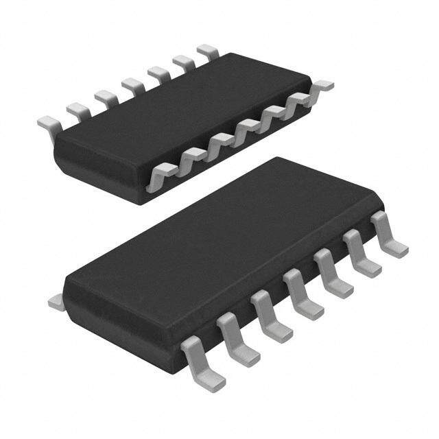
| 供应商器件封装 | 14-PDIP |
| 其它名称 | 296-33604-5 |
| 包装 | 管件 |
| 单位重量 | 1 g |
| 商标 | Texas Instruments |
| 安装类型 | 通孔 |
| 安装风格 | Through Hole |
| 封装 | Tube |
| 封装/外壳 | 14-DIP(0.300",7.62mm) |
| 封装/箱体 | PDIP-14 |
| 工作温度 | 0°C ~ 70°C |
| 工作温度范围 | 0 C to + 70 C |
| 工厂包装数量 | 25 |
| 最大工作温度 | + 70 C |
| 最小工作温度 | 0 C |
| 标准包装 | 25 |
| 特性 | 施密特触发器 |
| 电压-电源 | 4.75 V ~ 5.25 V |
| 电流-输出高,低 | 800µA, 16mA |
| 电流-静态(最大值) | - |
| 电源电压-最大 | 5.25 V |
| 电源电压-最小 | 4.75 V |
| 电路数 | 6 |
| 电路数量 | 6 Circuit |
| 系列 | SN7414 |
| 输入数 | 6 |
| 输入类型 | TTL |
| 输出类型 | CMOS |
| 逻辑电平-低 | 0.6V |
| 逻辑电平-高 | 2V |
| 逻辑类型 | |
| 逻辑系列 | TTL |
| 高电平输出电流 | - 0.8 mA |


- 商务部:美国ITC正式对集成电路等产品启动337调查
- 曝三星4nm工艺存在良率问题 高通将骁龙8 Gen1或转产台积电
- 太阳诱电将投资9.5亿元在常州建新厂生产MLCC 预计2023年完工
- 英特尔发布欧洲新工厂建设计划 深化IDM 2.0 战略
- 台积电先进制程称霸业界 有大客户加持明年业绩稳了
- 达到5530亿美元!SIA预计今年全球半导体销售额将创下新高
- 英特尔拟将自动驾驶子公司Mobileye上市 估值或超500亿美元
- 三星加码芯片和SET,合并消费电子和移动部门,撤换高东真等 CEO
- 三星电子宣布重大人事变动 还合并消费电子和移动部门
- 海关总署:前11个月进口集成电路产品价值2.52万亿元 增长14.8%


PDF Datasheet 数据手册内容提取
Product Sample & Technical Tools & Support & Folder Buy Documents Software Community SN5414,SN54LS14,SN7414,SN74LS14 SDLS049C–DECEMBER1983–REVISEDNOVEMBER2016 SNx414 and SNx4LS14 Hex Schmitt-Trigger Inverters 1 Features 3 Description • OperationFromVerySlowEdges Each circuit in SNx414 and SNx4LS14 functions as 1 an inverter. However, because of the Schmitt-Trigger • ImprovedLine-ReceivingCharacteristics action, they have different input threshold levels for • HighNoiseImmunity positive-going(V )andnegative-going(V )signals. T+ T– These circuits are temperature compensated and can 2 Applications be triggered from the slowest of input ramps and still • HVACGateways giveclean,jitter-freeoutputsignals. • ResidentialDuctlessAirConditioningOutdoor DeviceInformation(1) Units PARTNUMBER PACKAGE BODYSIZE(NOM) • RoboticControls SOIC(14) 4.90mm×3.91mm • IndustrialStepperMotors SN7414, SSOP(14) 6.20mm×5.30mm • PowerMeterandPowerAnalyzers SN74LS14 PDIP(14) 19.30mm×6.35mm • DigitalInputModulesforFactoryAutomation SO(14) 10.30mm×5.30mm CDIP(14) 19.56mm×6.67mm SN5414, CFP(14) 9.21mm×5.97mm SN54LS14 LCCC(20) 8.89mm×8.89mm (1) For all available packages, see the orderable addendum at theendofthedatasheet. LogicDiagram(PositiveLogic) A Y Copyright © 2016,Texas Instruments Incorporated 1 An IMPORTANT NOTICE at the end of this data sheet addresses availability, warranty, changes, use in safety-critical applications, intellectualpropertymattersandotherimportantdisclaimers.PRODUCTIONDATA.
SN5414,SN54LS14,SN7414,SN74LS14 SDLS049C–DECEMBER1983–REVISEDNOVEMBER2016 www.ti.com Table of Contents 1 Features.................................................................. 1 8.3 FeatureDescription.................................................13 2 Applications........................................................... 1 8.4 DeviceFunctionalModes........................................13 3 Description............................................................. 1 9 ApplicationandImplementation........................ 14 4 RevisionHistory..................................................... 2 9.1 ApplicationInformation............................................14 9.2 TypicalApplication..................................................14 5 PinConfigurationandFunctions......................... 3 9.3 SystemExamples...................................................16 6 Specifications......................................................... 4 10 PowerSupplyRecommendations..................... 17 6.1 AbsoluteMaximumRatings......................................4 11 Layout................................................................... 17 6.2 ESDRatings..............................................................4 6.3 RecommendedOperatingConditions.......................4 11.1 LayoutGuidelines.................................................17 6.4 ThermalInformation..................................................4 11.2 LayoutExample....................................................17 6.5 ElectricalCharacteristics...........................................5 12 DeviceandDocumentationSupport................. 18 6.6 SwitchingCharacteristics..........................................5 12.1 RelatedLinks........................................................18 6.7 TypicalCharacteristics..............................................6 12.2 ReceivingNotificationofDocumentationUpdates18 7 ParameterMeasurementInformation..................9 12.3 CommunityResources..........................................18 7.1 SeriesSN5414andSN7414Devices.......................9 12.4 Trademarks...........................................................18 7.2 SeriesSN54LS14andSN74LS14Devices............11 12.5 ElectrostaticDischargeCaution............................18 12.6 Glossary................................................................18 8 DetailedDescription............................................ 13 13 Mechanical,Packaging,andOrderable 8.1 Overview.................................................................13 Information........................................................... 18 8.2 FunctionalBlockDiagram.......................................13 4 Revision History ChangesfromRevisionB(February2002)toRevisionC Page • AddedESDRatingstable,FeatureDescriptionsection,DeviceFunctionalModes,ApplicationandImplementation section,PowerSupplyRecommendationssection,Layoutsection,DeviceandDocumentationSupportsection,and Mechanical,Packaging,andOrderableInformationsection.................................................................................................. 1 • DeletedOrderingInformationtable;seethePackageOptionAddendumattheendofthedatasheet ............................... 1 • ChangedPackagethermalimpedance,R ,valuesinThermalInformationtableFrom:86°C/WTo:90.1°C/W(D), θJA From:96°C/WTo:105.4°C/W(DB),From:80°C/WTo:54.9°C/W(N),andFrom:76°C/WTo:88.8°C/W(NS)...................4 2 SubmitDocumentationFeedback Copyright©1983–2016,TexasInstrumentsIncorporated ProductFolderLinks:SN5414 SN54LS14 SN7414 SN74LS14
SN5414,SN54LS14,SN7414,SN74LS14 www.ti.com SDLS049C–DECEMBER1983–REVISEDNOVEMBER2016 5 Pin Configuration and Functions D,DB,N,NS,J,orWPackage FKPackage 14-PinSOIC,SSOP,PDIP,SO,CDIP,orCFP 20-PinLCCC TopView TopView C 1Y 1A NC VC 6A 1A 1 14 VCC 1Y 2 13 6A 3 2 1 0 9 2 1 2A 3 12 6Y 2A 4 18 6Y 2Y 4 11 5A NC 5 17 NC 3A 5 10 5Y 2Y 6 16 5A 3Y 6 9 4A NC 7 15 NC GND 7 8 4Y 3A 8 14 5Y Not to scale 9 10 11 12 13 Not to scale Y D C Y A 3 N N 4 4 G NC–Nointernalconnection PinFunctions PIN SOIC,SSOP,TVSOP,CDIP, I/O DESCRIPTION NAME LCCC PDIP,TSSOP,CFP 1A 1 2 I Channel1input 1Y 2 3 O Channel1output 2A 3 4 I Channel2input 2Y 4 6 O Channel2output 3A 5 8 I Channel3input 3Y 6 9 O Channel3output 4A 9 13 I Channel4input 4Y 8 12 O Channel4output 5A 11 16 I Channel5input 5Y 10 14 O Channel5output 6A 13 19 I Channel6input 6Y 12 18 O Channel6output GND 7 10 — Ground 1,5,7, NC — — Nointernalconnection 11,15,17 V 14 20 — Powersupply CC Copyright©1983–2016,TexasInstrumentsIncorporated SubmitDocumentationFeedback 3 ProductFolderLinks:SN5414 SN54LS14 SN7414 SN74LS14
SN5414,SN54LS14,SN7414,SN74LS14 SDLS049C–DECEMBER1983–REVISEDNOVEMBER2016 www.ti.com 6 Specifications 6.1 Absolute Maximum Ratings overoperatingfree-airtemperaturerange(unlessotherwisenoted)(1) MIN MAX UNIT Supplyvoltage,V (2) 7 V CC SNx414 5.5 Inputvoltage V SNx4LS14 7 Junctiontemperature,T 150 °C J Storagetemperature,T –65 150 °C stg (1) StressesbeyondthoselistedunderAbsoluteMaximumRatingsmaycausepermanentdamagetothedevice.Thesearestressratings only,whichdonotimplyfunctionaloperationofthedeviceattheseoranyotherconditionsbeyondthoseindicatedunderRecommended OperatingConditions.Exposuretoabsolute-maximum-ratedconditionsforextendedperiodsmayaffectdevicereliability. (2) Voltagevaluesarewithrespecttonetworkgroundterminal. 6.2 ESD Ratings VALUE UNIT Electrostatic Human-bodymodel(HBM),perANSI/ESDA/JEDECJS-001(1) ±1500 V V (ESD) discharge Charged-devicemodel(CDM),perJEDECspecificationJESD22-C101(2) ±2000 (1) JEDECdocumentJEP155statesthat500-VHBMallowssafemanufacturingwithastandardESDcontrolprocess. (2) JEDECdocumentJEP157statesthat250-VCDMallowssafemanufacturingwithastandardESDcontrolprocess. 6.3 Recommended Operating Conditions overoperatingfree-airtemperaturerange(unlessotherwisenoted) MIN NOM MAX UNIT SN5414,SN54LS14 4.5 5 5.5 V Supplyvoltage V CC SN7414,SN74LS14 4.75 5 5.25 SN5414,SN7414 –0.8 I High-leveloutputcurrent mA OH SN54LS14,SN74LS14 –0.4 SN5414,SN7414 16 I Low-leveloutputcurrent SN54LS14 4 mA OL SN74LS14 8 SN5414,SN54LS14 –55 125 T Operatingfree-airtemperature °C A SN7414,SN74LS14 0 70 6.4 Thermal Information SNx414,SNx4LS14 THERMALMETRIC(1) D(SOIC) DB(SSOP) N(PDIP) NS(SO) UNIT 14PINS 14PINS 14PINS 14PINS R Junction-to-ambientthermalresistance(2) 90.1 105.4 54.9 88.8 °C/W θJA R Junction-to-case(top)thermalresistance 50.3 57.3 42.5 46.5 °C/W θJC(top) R Junction-to-boardthermalresistance 44.3 52.7 34.7 47.5 °C/W θJB ψ Junction-to-topcharacterizationparameter 17.9 22.5 27.8 16.8 °C/W JT ψ Junction-to-boardcharacterizationparameter 44.1 52.2 34.6 47.2 °C/W JB (1) Formoreinformationabouttraditionalandnewthermalmetrics,seetheSemiconductorandICPackageThermalMetricsapplication report. (2) ThepackagetermalimpedanceiscalculatedinaccordancewithJESD51-7. 4 SubmitDocumentationFeedback Copyright©1983–2016,TexasInstrumentsIncorporated ProductFolderLinks:SN5414 SN54LS14 SN7414 SN74LS14
SN5414,SN54LS14,SN7414,SN74LS14 www.ti.com SDLS049C–DECEMBER1983–REVISEDNOVEMBER2016 6.5 Electrical Characteristics overoperatingfree-airtemperaturerange(unlessotherwisenoted) PARAMETER TESTCONDITIONS(1) MIN TYP(2) MAX UNIT SNx414 1.5 1.7 2 V V =5V V T+ CC SNx4LS14 1.4 1.6 1.9 SNx414 0.6 0.9 1.1 V V =5V V T– CC SNx4LS14 0.5 0.8 1 Hysteresis V =5V 0.4 0.8 V (V –V ) CC T+ T– V =MIN,I =–12mA,SNx414 –1.5 CC I V V IK V =MIN,I =–18mA,SNx4LS14 –1.5 CC I V =MIN,V =0.6V,I =–0.8mA,SNx414 2.4 3.4 CC I OH V V OH V =MIN,V =0.5V,I =–0.4mA,SNx4LS14 2.4 3.4 CC I OH V =MIN,V =2V,I =16mA,SNx414 0.2 0.4 CC I OL V I =4mA,SNx4LS14 0.25 0.4 V OL OL V =MIN,V =1.9V CC I I =8mA,SN74LS14 0.35 0.5 OL SNx414 –0.43 I V =5V,V =V mA T+ CC I T+ SNx4LS14 –0.14 SNx414 –0.56 I V =5V,V =V mA T– CC I T– SNx4LS14 –0.18 V =MAX,V =5.5V,SNx414 1 CC I I mA I V =MAX,V =7V,SNx4LS14 0.1 CC I V =MAX,V =2.4V,SNx414 40 CC IH I µA IH V =MAX,V =2.7V,SNx4LS14 20 CC IH SNx414 –0.8 –1.2 I V =MAX,V =0.4V mA IL CC IL SNx4LS14 –0.4 SNx414 –18 –55 I (3) V =MAX mA OS CC SNx4LS14 –20 –100 SNx414 22 36 I V =MAX mA CCH CC SNx4LS14 8.6 16 SNx414 39 60 I V =MAX mA CCL CC SNx4LS14 12 21 (1) ForconditionsshownasMINorMAX,usetheappropriatevaluespecifiedunderrecommendedoperatingconditions. (2) AlltypicalvaluesareatV =5VandT =25°C. CC A (3) Notmorethanoneoutputshouldbeshortedatatime. 6.6 Switching Characteristics V =5V,T =25°C,andoveroperatingfree-airtemperaturerange(unlessotherwisenoted;seeFigure20) CC A PARAMETER FROM(INPUT) TO(OUTPUT) TESTCONDITIONS MIN TYP MAX UNIT R =400ΩandC =15pF,or t A Y L L 15 22 ns PLH R =2kΩandC =15pF L L R =400ΩandC =15pF,or t A Y L L 15 22 ns PHL R =2kΩandC =15pF L L Copyright©1983–2016,TexasInstrumentsIncorporated SubmitDocumentationFeedback 5 ProductFolderLinks:SN5414 SN54LS14 SN7414 SN74LS14
SN5414,SN54LS14,SN7414,SN74LS14 SDLS049C–DECEMBER1983–REVISEDNOVEMBER2016 www.ti.com 6.7 Typical Characteristics 6.7.1 SNx414Circuits Data for temperatures below 0°C and above 70°C and supply voltage below 4.75 V and above 5.25 V are applicableforSN5414only. 1.70 0.90 V VCC=5 V V VCC=5 V – 1.69 – 0.89 Voltage 1.68 Voltage 0.88 Threshold 11..6667 Threshold 00..8867 –Positive-Going 1111....66664253 –Negative-Going 0000....88884253 VT+ 1.61 VT– 0.81 1.60 0.80 –75 –50 –25 0 25 50 75 100 125 –75 –50 –25 0 25 50 75 100 125 TA–Free-Air Temperature–°C TA–Free-Air Temperature–°C Figure1.Positive-GoingThresholdVoltage Figure2.Negative-GoingThresholdVoltage vsFree-AirTemperature vsFree-AirTemperature 850 840 VCC=5 V VTACC= =255° CV 830 nce mV 820 ure Hysteresis– 881000 uencyofOcc –VVT+–T– 777978000 RelativeFreq 760 750 –75 –50 –25 0 25 50 75 100 125 740 760 780 800 820 840 860 880 900 TA–Free-Air Temperature–°C VT+–VT––Hysteresis–mV Figure3.HysteresisvsFree-AirTemperature Figure4.DistributionofUnitsforHysteresis 2.0 2.0 TA= 25°C TA= 25°C 1.8 1.8 1.6 V 1.6 ThresholdVoltage-–V 01110.....82406 PoNsietigvaet-iGveo-iGngoiTnhgrTehshreosldhoVlodltVaogleta,gVeT,+VT– –HyVVsteresis–T+–T– 01110.....82406 0.4 0.4 0.2 0.2 0 0 4.5 4.75 5 5.25 5.5 4.5 4.75 5 5.25 5.5 VT+–VT––Hysteresis–mV VCC–Supply Voltage–V Figure5.ThresholdVoltagesvsSupplyVoltage Figure6.HysteresisvsSupplyVoltage 6 SubmitDocumentationFeedback Copyright©1983–2016,TexasInstrumentsIncorporated ProductFolderLinks:SN5414 SN54LS14 SN7414 SN74LS14
SN5414,SN54LS14,SN7414,SN74LS14 www.ti.com SDLS049C–DECEMBER1983–REVISEDNOVEMBER2016 SNx414 Circuits (continued) 4 VCC=5 V TA= 25°C VT– VT+ V 3 – ge Volta put 2 ut O – O V 1 0 0 0.4 0.8 1.2 1.6 2 VCC–Supply Voltage–V Figure7.OutputVoltagevsInputVoltage Copyright©1983–2016,TexasInstrumentsIncorporated SubmitDocumentationFeedback 7 ProductFolderLinks:SN5414 SN54LS14 SN7414 SN74LS14
SN5414,SN54LS14,SN7414,SN74LS14 SDLS049C–DECEMBER1983–REVISEDNOVEMBER2016 www.ti.com 6.7.2 SNx4LS14Circuits Data for temperatures below 0°C and above 70°C and supply voltage below 4.75 V and above 5.25 V are applicableforSNx4LS14only. 1.70 0.90 –V 1.69 VCC=5 V V– 0.89 VCC=5 V Voltage 1.68 oltageV 0.88 GoingThreshold 1111....66664675 GoingThreshold 0000....88884675 Positive- 11..6623 Negative- 00..8823 – – VT+ 1.61 VT– 0.81 1.60 0.80 –75 –50 –25 0 25 50 75 100 125 –75 –50 –25 0 25 50 75 100 125 TA–Free-Air Temperature–°C TA–Free-Air Temperature–°C Figure8.Positive-GoingThresholdVoltage Figure9.Negative-GoingThresholdVoltage vsFree-AirTemperature vsFree-AirTemperature 850 840 VCC=5 V VTACC= =255° CV V 830 nce –HystVVeresis–T+–T– 778887971208000000 RelativeFrequencyofOccure 9A9B%OAVREE 735mV 760 750 –75 –50 –25 0 25 50 75 100 125 720 740 760 780 800 820 840 860 880 TA–Free-Air Temperature–°C VT+–VT––Hysteresis–mV Figure10.HysteresisvsFree-AirTemperature Figure11.DistributionofUnitsforHysteresis 2.0 4 1.8 TA= 25°C VTACC= =255° CV VT– VT+ 1.6 ThresholdVoltage–V 01110.....82406 NegatPivoes-iGtivoein-GgoTihnrgeHsTyhhsorteledsrheVosoillsdta,VgVoeTl,+taV–gTeV–,TV–T+ –OVutputVoltage–VO 23 1 0.4 0.2 0 0 4.5 4.75 5 5.25 5.5 0 0.4 0.8 1.2 1.6 2 VCC–Supply Voltage–V VI–Input Voltage–V Figure12.ThresholdVoltagesandHysteresis Figure13.OutputVoltagevsInputVoltage vsSupplyVoltage 8 SubmitDocumentationFeedback Copyright©1983–2016,TexasInstrumentsIncorporated ProductFolderLinks:SN5414 SN54LS14 SN7414 SN74LS14
SN5414,SN54LS14,SN7414,SN74LS14 www.ti.com SDLS049C–DECEMBER1983–REVISEDNOVEMBER2016 7 Parameter Measurement Information 7.1 Series SN5414 and SN7414 Devices Test VCC Point VCC RL RL FromOutput Test FromOutput UnderTest Point UnderTest CL CL Figure14.LoadCircuitFor Figure15.LoadCircuitFor 2-StateTotem-PoleOutputs Open-CollectorOutputs VCC High-Level Test RL Pulse 1.5V 1.5V Point S1 FromOutput tw UnderTest Low-Level CL 1.5V 1.5V Pulse 1kΩ S2 Figure16.LoadCircuitFor3-StateOutputs Figure17.VoltageWaveformsPulseDurations 3V 3V Timing 1.5V Input 1.5V 1.5V Input 0V 0V th tsu tPLH tPHL 3V Data In-Phase VOH Input 1.5V 1.5V Output 1.5V 1.5V 0V VOL tPHL tPLH Out-of-Phase VOH Output 1.5V 1.5V VOL Figure18.VoltageWaveforms Figure19.VoltageWaveforms SetupandHoldTimes PropagationDelayTimes Copyright©1983–2016,TexasInstrumentsIncorporated SubmitDocumentationFeedback 9 ProductFolderLinks:SN5414 SN54LS14 SN7414 SN74LS14
SN5414,SN54LS14,SN7414,SN74LS14 SDLS049C–DECEMBER1983–REVISEDNOVEMBER2016 www.ti.com Series SN5414 and SN7414 Devices (continued) Output 3V Control 1.5V 1.5V (low-level enabling) 0V tPZL tPLZ Waveform1 ≈1.5V 1.5V VOL+ 0.5V VOL tPZH tPHZ VOH Waveform2 VOH–0.5 V 1.5V ≈1.5V A. C includesprobeandjigcapacitance. L B. Alldiodesare1N3064orequivalent. C. Waveform1 is for an outputwith internalconditions such that theoutputis lowexceptwhendisabledby theoutput control.Waveform2isforanoutputwithinternalconditionssuchthattheoutputishighexceptwhendisabledbythe outputcontrol. D. S1andS2areclosedfort ,t ,t ,andt ;S1isopenandS2isclosedfort ;S1isclosedandS2isopen PLH PHL PHZ PLZ PZH fort . PZL E. Allinputpulsesaresuppliedbygeneratorshavingthefollowingcharacteristics:PRR≤1MHz,Z ≈50Ω;t andt ≤7 O r f nsforSeriesSN5414andSN7414devicesandt andt ≤2.5nsforSeriesSN54S14andSN74S14devices. r f F. Theoutputsaremeasuredoneatatimewithoneinputtransitionpermeasurement. Figure20. VoltageWaveformsEnableandDisableTimes,3-StateOutputs 10 SubmitDocumentationFeedback Copyright©1983–2016,TexasInstrumentsIncorporated ProductFolderLinks:SN5414 SN54LS14 SN7414 SN74LS14
SN5414,SN54LS14,SN7414,SN74LS14 www.ti.com SDLS049C–DECEMBER1983–REVISEDNOVEMBER2016 7.2 Series SN54LS14 and SN74LS14 Devices Test VCC Point VCC RL RL FromOutput Test FromOutput UnderTest Point UnderTest CL CL Figure21.LoadCircuitFor Figure22.LoadCircuitFor 2-StateTotem-PoleOutputs Open-CollectorOutputs VCC High-Level Test RL Pulse 1.3V 1.3V Point S1 FromOutput tw UnderTest Low-Level CL 1.3V 1.3V Pulse 5kΩ S2 Figure23.LoadCircuitFor3-StateOutputs Figure24.VoltageWaveformsPulseDurations 3V 3V Timing 1.3V Input 1.3V 1.3V Input 0V 0V th tsu tPLH tPHL 3V Data In-Phase VOH Input 1.3V 1.3V Output 1.3V 1.3V 0V VOL tPHL tPLH Out-of-Phase VOH Output 1.3V 1.3V VOL Figure25.VoltageWaveforms Figure26.VoltageWaveforms SetupandHoldTimes PropagationDelayTimes Copyright©1983–2016,TexasInstrumentsIncorporated SubmitDocumentationFeedback 11 ProductFolderLinks:SN5414 SN54LS14 SN7414 SN74LS14
SN5414,SN54LS14,SN7414,SN74LS14 SDLS049C–DECEMBER1983–REVISEDNOVEMBER2016 www.ti.com Series SN54LS14 and SN74LS14 Devices (continued) Output 3V Control 1.3V 1.3V (low-level enabling) 0V tPZL tPLZ Waveform1 ≈1.5V 1.3V VOL+ 0.5V VOL tPZH tPHZ VOH Waveform2 VOH–0.5 V 1.3V ≈1.5V A. C includesprobeandjigcapacitance. L B. Alldiodesare1N3064orequivalent. C. Waveform1 is for an outputwith internalconditions such that theoutputis lowexceptwhendisabledby theoutput control.Waveform2isforanoutputwithinternalconditionssuchthattheoutputishighexceptwhendisabledbythe outputcontrol. D. S1andS2areclosedfort ,t ,t ,andt ;S1isopenandS2isclosedfort ;S1isclosedandS2isopen PLH PHL PHZ PLZ PZH fort . PZL E. Phaserelationshipsbetweeninputsandoutputshavebeenchosenarbitrarilyfortheseexamples. F. Allinputpulsesaresuppliedbygeneratorshavingthefollowingcharacteristics:PRR≤1MHz,Z ≈50Ω,t ≤1.5ns, O r t ≤2.6ns. f G. Theoutputsaremeasuredoneatatimewithoneinputtransitionpermeasurement. Figure27. VoltageWaveformsEnableandDisableTimes,3-StateOutputs 12 SubmitDocumentationFeedback Copyright©1983–2016,TexasInstrumentsIncorporated ProductFolderLinks:SN5414 SN54LS14 SN7414 SN74LS14
SN5414,SN54LS14,SN7414,SN74LS14 www.ti.com SDLS049C–DECEMBER1983–REVISEDNOVEMBER2016 8 Detailed Description 8.1 Overview The SNx414 and SNx4LS14 Schmitt-Trigger devices contain six independent inverters. They perform the BooleanfunctionY= Ainpositivelogic. Schmitt-Trigger inputs are designed to provide a minimum separation between positive and negative switching thresholds. This allows for noisy or slow inputs that would cause problems such as oscillation or excessive currentdrawwithnormalCMOSinputs. 8.2 Functional Block Diagram A Y Copyright © 2016,Texas Instruments Incorporated 8.3 Feature Description Thedevicecanoperatefromveryslowtransitionedgeinputs.Thisdevicehashighnoiseimmunity. 8.4 Device Functional Modes Table1liststhefunctionalmodesoftheSNx414andSNx4LS14. Table1.FunctionTable INPUTA OUTPUTY H L L H Copyright©1983–2016,TexasInstrumentsIncorporated SubmitDocumentationFeedback 13 ProductFolderLinks:SN5414 SN54LS14 SN7414 SN74LS14
SN5414,SN54LS14,SN7414,SN74LS14 SDLS049C–DECEMBER1983–REVISEDNOVEMBER2016 www.ti.com 9 Application and Implementation NOTE Information in the following applications sections is not part of the TI component specification, and TI does not warrant its accuracy or completeness. TI’s customers are responsible for determining suitability of components for their purposes. Customers should validateandtesttheirdesignimplementationtoconfirmsystemfunctionality. 9.1 Application Information The SNx414 and SNx4LS14 device is a Schmitt-Trigger input CMOS device that can be used for a multitude of inverting buffer type functions. The application shown here takes advantage of the Schmitt-Trigger inputs to produceadelayforalogicinput. 9.2 Typical Application Copyright © 2016, Texas Instruments Incorporated Figure28. SimplifiedApplicationSchematic 9.2.1 DesignRequirements This device uses CMOS technology. Take care to avoid bus contention because it can drive currents that would exceed maximum limits. Parallel output drive can create fast edges into light loads, so consider routing and load conditionstopreventringing. 9.2.2 DetailedDesignProcedure This circuit is designed around an RC network that produces a slow input to the second inverter. The RC time constant(τ)iscalculatedfrom: τ=RC. The delay time for this circuit is from t = –ln |1 – V / V | τ to t = –ln |1 – V / V | τ. It delay(min) T+(min) CC delay(max) T+(max) CC must be noted that the delay is consistent for each device, but because the switching threshold is only ensured between the minimum and maximum value, the output pulse length varies between devices. These values must becalculatedbyusingtheminimumandmaximumensuredV valuesintheElectricalCharacteristics. T+ TheresistorvaluemustbechosensuchthatthemaximumcurrenttoandfromtheSNx414/SNx4LS14is8mAat 5-VV . CC 14 SubmitDocumentationFeedback Copyright©1983–2016,TexasInstrumentsIncorporated ProductFolderLinks:SN5414 SN54LS14 SN7414 SN74LS14
SN5414,SN54LS14,SN7414,SN74LS14 www.ti.com SDLS049C–DECEMBER1983–REVISEDNOVEMBER2016 Typical Application (continued) 9.2.3 ApplicationCurve V CC V T+(max) e g V Typical a T+ Volt VT+ V T+(min) V t (cid:16)ln|1(cid:16) T(cid:14)(max)|W delay(max) VCC VC V tdelay(min) (cid:16)ln|1(cid:16) TV(cid:14)(min) |W VOUT CC 0.0 t0 t0 + 2(cid:3) t0 + 22(cid:3) t0 + 32(cid:3) t0 + 42(cid:3) t0 + 52(cid:3) Time Figure29.IdealCapacitorVoltageandOutputVoltageWithPositiveSwitchingThreshold Copyright©1983–2016,TexasInstrumentsIncorporated SubmitDocumentationFeedback 15 ProductFolderLinks:SN5414 SN54LS14 SN7414 SN74LS14
SN5414,SN54LS14,SN7414,SN74LS14 SDLS049C–DECEMBER1983–REVISEDNOVEMBER2016 www.ti.com 9.3 System Examples HerearesomeexamplesofvariousapplicationsusingtheSNx414andSNx4LS14device. VT+ TTLSystem Input VT– CMOS Sine-Wave Oscillator Output Figure30.TTLSystemInterfaceForSlowInput Figure31.PulseShaper Waveforms 0.1 Hzto 10MHz 330Ω VT+ VT– Input Input Output Figure32.Multivibrator Figure33.ThresholdDetector Open-Collector Input Output Input A Output VT+ PointA Output Figure34. PulseStretcher 16 SubmitDocumentationFeedback Copyright©1983–2016,TexasInstrumentsIncorporated ProductFolderLinks:SN5414 SN54LS14 SN7414 SN74LS14
SN5414,SN54LS14,SN7414,SN74LS14 www.ti.com SDLS049C–DECEMBER1983–REVISEDNOVEMBER2016 10 Power Supply Recommendations The power supply can be any voltage between the minimum and maximum supply voltage rating located in the Recommended Operating Conditions. The V terminal must have a good bypass capacitor to prevent power CC disturbance. TI recommends using a 0.1-µF capacitor on the V terminal, and must be placed as close as CC possibletothepinforbestresults. 11 Layout 11.1 Layout Guidelines When using multiple bit logic devices, inputs must never float. In many cases, functions or parts of functions of digital logic devices are unused, for example, when only two inputs of a triple-input AND gate are used or only three of the four buffer gates are used. Such inputs must not be left unconnected because the undefined voltages at the outside connections result in undefined operational states. All unused inputs of digital logic devices must be connected to a high or low bias to prevent them from floating. The logic level that must be applied to any particular unused input depends on the function of the device. Generally they are tied to GND or V , whichever makes more sense or is more convenient. Floating outputs are generally acceptable, unless the CC partisatransceiver. 11.2 Layout Example V cc Input Unused Input Output Unused Input Output Input Figure35. LayoutDiagram Copyright©1983–2016,TexasInstrumentsIncorporated SubmitDocumentationFeedback 17 ProductFolderLinks:SN5414 SN54LS14 SN7414 SN74LS14
SN5414,SN54LS14,SN7414,SN74LS14 SDLS049C–DECEMBER1983–REVISEDNOVEMBER2016 www.ti.com 12 Device and Documentation Support 12.1 Related Links The table below lists quick access links. Categories include technical documents, support and community resources,toolsandsoftware,andquickaccesstosampleorbuy. Table2.RelatedLinks TECHNICAL TOOLS& SUPPORT& PARTS PRODUCTFOLDER SAMPLE&BUY DOCUMENTS SOFTWARE COMMUNITY SN5414 Clickhere Clickhere Clickhere Clickhere Clickhere SN54LS14 Clickhere Clickhere Clickhere Clickhere Clickhere SN7414 Clickhere Clickhere Clickhere Clickhere Clickhere SN74LS14 Clickhere Clickhere Clickhere Clickhere Clickhere 12.2 Receiving Notification of Documentation Updates To receive notification of documentation updates, navigate to the device product folder on ti.com. In the upper right corner, click on Alert me to register and receive a weekly digest of any product information that has changed.Forchangedetails,reviewtherevisionhistoryincludedinanyreviseddocument. 12.3 Community Resources The following links connect to TI community resources. Linked contents are provided "AS IS" by the respective contributors. They do not constitute TI specifications and do not necessarily reflect TI's views; see TI's Terms of Use. TIE2E™OnlineCommunity TI'sEngineer-to-Engineer(E2E)Community.Createdtofostercollaboration amongengineers.Ate2e.ti.com,youcanaskquestions,shareknowledge,exploreideasandhelp solveproblemswithfellowengineers. DesignSupport TI'sDesignSupport QuicklyfindhelpfulE2Eforumsalongwithdesignsupporttoolsand contactinformationfortechnicalsupport. 12.4 Trademarks E2EisatrademarkofTexasInstruments. Allothertrademarksarethepropertyoftheirrespectiveowners. 12.5 Electrostatic Discharge Caution Thesedeviceshavelimitedbuilt-inESDprotection.Theleadsshouldbeshortedtogetherorthedeviceplacedinconductivefoam duringstorageorhandlingtopreventelectrostaticdamagetotheMOSgates. 12.6 Glossary SLYZ022—TIGlossary. Thisglossarylistsandexplainsterms,acronyms,anddefinitions. 13 Mechanical, Packaging, and Orderable Information The following pages include mechanical, packaging, and orderable information. This information is the most current data available for the designated devices. This data is subject to change without notice and revision of thisdocument.Forbrowser-basedversionsofthisdatasheet,refertotheleft-handnavigation. 18 SubmitDocumentationFeedback Copyright©1983–2016,TexasInstrumentsIncorporated ProductFolderLinks:SN5414 SN54LS14 SN7414 SN74LS14
PACKAGE OPTION ADDENDUM www.ti.com 28-Jul-2020 PACKAGING INFORMATION Orderable Device Status Package Type Package Pins Package Eco Plan Lead finish/ MSL Peak Temp Op Temp (°C) Device Marking Samples (1) Drawing Qty (2) Ball material (3) (4/5) (6) 5962-9665801Q2A ACTIVE LCCC FK 20 1 TBD POST-PLATE N / A for Pkg Type -55 to 125 5962- 9665801Q2A SNJ54LS 14FK 5962-9665801QCA ACTIVE CDIP J 14 1 TBD SNPB N / A for Pkg Type -55 to 125 5962-9665801QC A SNJ54LS14J 5962-9665801QDA ACTIVE CFP W 14 1 TBD Call TI N / A for Pkg Type -55 to 125 5962-9665801QD A SNJ54LS14W 5962-9665801VDA ACTIVE CFP W 14 1 TBD Call TI N / A for Pkg Type -55 to 125 5962-9665801VD A SNV54LS14W JM38510/31302BCA ACTIVE CDIP J 14 1 TBD SNPB N / A for Pkg Type -55 to 125 JM38510/ 31302BCA M38510/31302BCA ACTIVE CDIP J 14 1 TBD SNPB N / A for Pkg Type -55 to 125 JM38510/ 31302BCA SN5414J ACTIVE CDIP J 14 1 TBD SNPB N / A for Pkg Type -55 to 125 SN5414J SN54LS14J ACTIVE CDIP J 14 1 TBD SNPB N / A for Pkg Type -55 to 125 SN54LS14J SN7414D ACTIVE SOIC D 14 50 Green (RoHS NIPDAU Level-1-260C-UNLIM 0 to 70 7414 & no Sb/Br) SN7414DG4 ACTIVE SOIC D 14 50 Green (RoHS NIPDAU Level-1-260C-UNLIM 0 to 70 7414 & no Sb/Br) SN7414DR ACTIVE SOIC D 14 2500 Green (RoHS NIPDAU Level-1-260C-UNLIM 0 to 70 7414 & no Sb/Br) SN7414N ACTIVE PDIP N 14 25 Green (RoHS NIPDAU N / A for Pkg Type 0 to 70 SN7414N & no Sb/Br) SN7414NSR ACTIVE SO NS 14 2000 Green (RoHS NIPDAU Level-1-260C-UNLIM 0 to 70 SN7414 & no Sb/Br) SN74LS14D ACTIVE SOIC D 14 50 Green (RoHS NIPDAU Level-1-260C-UNLIM 0 to 70 LS14 & no Sb/Br) SN74LS14DBR ACTIVE SSOP DB 14 2000 Green (RoHS NIPDAU Level-1-260C-UNLIM 0 to 70 LS14 & no Sb/Br) Addendum-Page 1
PACKAGE OPTION ADDENDUM www.ti.com 28-Jul-2020 Orderable Device Status Package Type Package Pins Package Eco Plan Lead finish/ MSL Peak Temp Op Temp (°C) Device Marking Samples (1) Drawing Qty (2) Ball material (3) (4/5) (6) SN74LS14DE4 ACTIVE SOIC D 14 50 Green (RoHS NIPDAU Level-1-260C-UNLIM 0 to 70 LS14 & no Sb/Br) SN74LS14DG4 ACTIVE SOIC D 14 50 Green (RoHS NIPDAU Level-1-260C-UNLIM 0 to 70 LS14 & no Sb/Br) SN74LS14DR ACTIVE SOIC D 14 2500 Green (RoHS NIPDAU Level-1-260C-UNLIM 0 to 70 LS14 & no Sb/Br) SN74LS14DRE4 ACTIVE SOIC D 14 2500 Green (RoHS NIPDAU Level-1-260C-UNLIM 0 to 70 LS14 & no Sb/Br) SN74LS14DRG4 ACTIVE SOIC D 14 2500 Green (RoHS NIPDAU Level-1-260C-UNLIM 0 to 70 LS14 & no Sb/Br) SN74LS14N ACTIVE PDIP N 14 25 Green (RoHS NIPDAU N / A for Pkg Type 0 to 70 SN74LS14N & no Sb/Br) SN74LS14NE4 ACTIVE PDIP N 14 25 Green (RoHS NIPDAU N / A for Pkg Type 0 to 70 SN74LS14N & no Sb/Br) SN74LS14NSR ACTIVE SO NS 14 2000 Green (RoHS NIPDAU Level-1-260C-UNLIM 0 to 70 74LS14 & no Sb/Br) SNJ5414J ACTIVE CDIP J 14 1 TBD SNPB N / A for Pkg Type -55 to 125 SNJ5414J SNJ5414W ACTIVE CFP W 14 1 TBD Call TI N / A for Pkg Type -55 to 125 SNJ5414W SNJ54LS14FK ACTIVE LCCC FK 20 1 TBD POST-PLATE N / A for Pkg Type -55 to 125 5962- 9665801Q2A SNJ54LS 14FK SNJ54LS14J ACTIVE CDIP J 14 1 TBD SNPB N / A for Pkg Type -55 to 125 5962-9665801QC A SNJ54LS14J SNJ54LS14W ACTIVE CFP W 14 1 TBD Call TI N / A for Pkg Type -55 to 125 5962-9665801QD A SNJ54LS14W (1) The marketing status values are defined as follows: ACTIVE: Product device recommended for new designs. LIFEBUY: TI has announced that the device will be discontinued, and a lifetime-buy period is in effect. NRND: Not recommended for new designs. Device is in production to support existing customers, but TI does not recommend using this part in a new design. PREVIEW: Device has been announced but is not in production. Samples may or may not be available. OBSOLETE: TI has discontinued the production of the device. Addendum-Page 2
PACKAGE OPTION ADDENDUM www.ti.com 28-Jul-2020 (2) RoHS: TI defines "RoHS" to mean semiconductor products that are compliant with the current EU RoHS requirements for all 10 RoHS substances, including the requirement that RoHS substance do not exceed 0.1% by weight in homogeneous materials. Where designed to be soldered at high temperatures, "RoHS" products are suitable for use in specified lead-free processes. TI may reference these types of products as "Pb-Free". RoHS Exempt: TI defines "RoHS Exempt" to mean products that contain lead but are compliant with EU RoHS pursuant to a specific EU RoHS exemption. Green: TI defines "Green" to mean the content of Chlorine (Cl) and Bromine (Br) based flame retardants meet JS709B low halogen requirements of <=1000ppm threshold. Antimony trioxide based flame retardants must also meet the <=1000ppm threshold requirement. (3) MSL, Peak Temp. - The Moisture Sensitivity Level rating according to the JEDEC industry standard classifications, and peak solder temperature. (4) There may be additional marking, which relates to the logo, the lot trace code information, or the environmental category on the device. (5) Multiple Device Markings will be inside parentheses. Only one Device Marking contained in parentheses and separated by a "~" will appear on a device. If a line is indented then it is a continuation of the previous line and the two combined represent the entire Device Marking for that device. (6) Lead finish/Ball material - Orderable Devices may have multiple material finish options. Finish options are separated by a vertical ruled line. Lead finish/Ball material values may wrap to two lines if the finish value exceeds the maximum column width. Important Information and Disclaimer:The information provided on this page represents TI's knowledge and belief as of the date that it is provided. TI bases its knowledge and belief on information provided by third parties, and makes no representation or warranty as to the accuracy of such information. Efforts are underway to better integrate information from third parties. TI has taken and continues to take reasonable steps to provide representative and accurate information but may not have conducted destructive testing or chemical analysis on incoming materials and chemicals. TI and TI suppliers consider certain information to be proprietary, and thus CAS numbers and other limited information may not be available for release. In no event shall TI's liability arising out of such information exceed the total purchase price of the TI part(s) at issue in this document sold by TI to Customer on an annual basis. OTHER QUALIFIED VERSIONS OF SN5414, SN54LS14, SN54LS14-SP, SN7414, SN74LS14 : •Catalog: SN7414, SN74LS14, SN54LS14 •Military: SN5414, SN54LS14 •Space: SN54LS14-SP NOTE: Qualified Version Definitions: •Catalog - TI's standard catalog product •Military - QML certified for Military and Defense Applications Addendum-Page 3
PACKAGE OPTION ADDENDUM www.ti.com 28-Jul-2020 •Space - Radiation tolerant, ceramic packaging and qualified for use in Space-based application Addendum-Page 4
PACKAGE MATERIALS INFORMATION www.ti.com 20-Dec-2018 TAPE AND REEL INFORMATION *Alldimensionsarenominal Device Package Package Pins SPQ Reel Reel A0 B0 K0 P1 W Pin1 Type Drawing Diameter Width (mm) (mm) (mm) (mm) (mm) Quadrant (mm) W1(mm) SN7414DR SOIC D 14 2500 330.0 16.4 6.5 9.0 2.1 8.0 16.0 Q1 SN7414NSR SO NS 14 2000 330.0 16.4 8.2 10.5 2.5 12.0 16.0 Q1 SN74LS14DR SOIC D 14 2500 330.0 16.4 6.5 9.0 2.1 8.0 16.0 Q1 SN74LS14NSR SO NS 14 2000 330.0 16.4 8.2 10.5 2.5 12.0 16.0 Q1 PackMaterials-Page1
PACKAGE MATERIALS INFORMATION www.ti.com 20-Dec-2018 *Alldimensionsarenominal Device PackageType PackageDrawing Pins SPQ Length(mm) Width(mm) Height(mm) SN7414DR SOIC D 14 2500 367.0 367.0 38.0 SN7414NSR SO NS 14 2000 367.0 367.0 38.0 SN74LS14DR SOIC D 14 2500 367.0 367.0 38.0 SN74LS14NSR SO NS 14 2000 367.0 367.0 38.0 PackMaterials-Page2
None
None
None
None
PACKAGE OUTLINE J0014A CDIP - 5.08 mm max height SCALE 0.900 CERAMIC DUAL IN LINE PACKAGE PIN 1 ID A 4X .005 MIN (OPTIONAL) [0.13] .015-.060 TYP [0.38-1.52] 1 14 12X .100 [2.54] 14X .014-.026 14X .045-.065 [0.36-0.66] [1.15-1.65] .010 [0.25] C A B .754-.785 [19.15-19.94] 7 8 B .245-.283 .2 MAX TYP .13 MIN TYP [6.22-7.19] [5.08] [3.3] SEATING PLANE C .308-.314 [7.83-7.97] AT GAGE PLANE .015 GAGE PLANE [0.38] 0 -15 14X .008-.014 TYP [0.2-0.36] 4214771/A 05/2017 NOTES: 1. All controlling linear dimensions are in inches. Dimensions in brackets are in millimeters. Any dimension in brackets or parenthesis are for reference only. Dimensioning and tolerancing per ASME Y14.5M. 2. This drawing is subject to change without notice. 3. This package is hermitically sealed with a ceramic lid using glass frit. 4. Index point is provided on cap for terminal identification only and on press ceramic glass frit seal only. 5. Falls within MIL-STD-1835 and GDIP1-T14. www.ti.com
EXAMPLE BOARD LAYOUT J0014A CDIP - 5.08 mm max height CERAMIC DUAL IN LINE PACKAGE (.300 ) TYP [7.62] SEE DETAIL B SEE DETAIL A 1 14 12X (.100 ) [2.54] SYMM 14X ( .039) [1] 7 8 SYMM LAND PATTERN EXAMPLE NON-SOLDER MASK DEFINED SCALE: 5X .002 MAX (.063) [0.05] [1.6] METAL ALL AROUND ( .063) SOLDER MASK [1.6] OPENING METAL .002 MAX SOLDER MASK (R.002 ) TYP [0.05] OPENING [0.05] ALL AROUND DETAIL A DETAIL B SCALE: 15X 13X, SCALE: 15X 4214771/A 05/2017 www.ti.com
None
None
None
MECHANICAL DATA MSSO002E – JANUARY 1995 – REVISED DECEMBER 2001 DB (R-PDSO-G**) PLASTIC SMALL-OUTLINE 28 PINS SHOWN 0,38 0,65 0,15 M 0,22 28 15 0,25 0,09 5,60 8,20 5,00 7,40 Gage Plane 1 14 0,25 A 0°–(cid:1)8° 0,95 0,55 Seating Plane 2,00 MAX 0,05 MIN 0,10 PINS ** 14 16 20 24 28 30 38 DIM A MAX 6,50 6,50 7,50 8,50 10,50 10,50 12,90 A MIN 5,90 5,90 6,90 7,90 9,90 9,90 12,30 4040065/E 12/01 NOTES: A. All linear dimensions are in millimeters. B. This drawing is subject to change without notice. C. Body dimensions do not include mold flash or protrusion not to exceed 0,15. D. Falls within JEDEC MO-150 • POST OFFICE BOX 655303 DALLAS, TEXAS 75265
IMPORTANTNOTICEANDDISCLAIMER TI PROVIDES TECHNICAL AND RELIABILITY DATA (INCLUDING DATASHEETS), DESIGN RESOURCES (INCLUDING REFERENCE DESIGNS), APPLICATION OR OTHER DESIGN ADVICE, WEB TOOLS, SAFETY INFORMATION, AND OTHER RESOURCES “AS IS” AND WITH ALL FAULTS, AND DISCLAIMS ALL WARRANTIES, EXPRESS AND IMPLIED, INCLUDING WITHOUT LIMITATION ANY IMPLIED WARRANTIES OF MERCHANTABILITY, FITNESS FOR A PARTICULAR PURPOSE OR NON-INFRINGEMENT OF THIRD PARTY INTELLECTUAL PROPERTY RIGHTS. These resources are intended for skilled developers designing with TI products. You are solely responsible for (1) selecting the appropriate TI products for your application, (2) designing, validating and testing your application, and (3) ensuring your application meets applicable standards, and any other safety, security, or other requirements. These resources are subject to change without notice. TI grants you permission to use these resources only for development of an application that uses the TI products described in the resource. Other reproduction and display of these resources is prohibited. No license is granted to any other TI intellectual property right or to any third party intellectual property right. TI disclaims responsibility for, and you will fully indemnify TI and its representatives against, any claims, damages, costs, losses, and liabilities arising out of your use of these resources. TI’s products are provided subject to TI’s Terms of Sale (www.ti.com/legal/termsofsale.html) or other applicable terms available either on ti.com or provided in conjunction with such TI products. TI’s provision of these resources does not expand or otherwise alter TI’s applicable warranties or warranty disclaimers for TI products. Mailing Address: Texas Instruments, Post Office Box 655303, Dallas, Texas 75265 Copyright © 2020, Texas Instruments Incorporated