ICGOO在线商城 > 集成电路(IC) > 接口 - 驱动器,接收器,收发器 > SN65LVDS348PWG4
 Datasheet下载
- 型号: SN65LVDS348PWG4
- 制造商: Texas Instruments
- 库位|库存: xxxx|xxxx
- 要求:
| 数量阶梯 | 香港交货 | 国内含税 |
| +xxxx | $xxxx | ¥xxxx |
查看当月历史价格
查看今年历史价格
SN65LVDS348PWG4产品简介:
ICGOO电子元器件商城为您提供SN65LVDS348PWG4由Texas Instruments设计生产,在icgoo商城现货销售,并且可以通过原厂、代理商等渠道进行代购。 SN65LVDS348PWG4价格参考¥20.77-¥20.77。Texas InstrumentsSN65LVDS348PWG4封装/规格:接口 - 驱动器,接收器,收发器, 接收器 0/4 LVDS 16-TSSOP。您可以下载SN65LVDS348PWG4参考资料、Datasheet数据手册功能说明书,资料中有SN65LVDS348PWG4 详细功能的应用电路图电压和使用方法及教程。
| 参数 | 数值 |
| 产品目录 | 集成电路 (IC)半导体 |
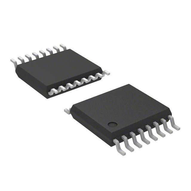
| 描述 | IC DIFF RECEIVER QUAD HS 16TSSOPLVDS 接口集成电路 Quad LVDS Receiver |
| 产品分类 | |
| 品牌 | Texas Instruments |
| 产品手册 | |
| 产品图片 |
|
| rohs | 符合RoHS无铅 / 符合限制有害物质指令(RoHS)规范要求 |
| 产品系列 | 接口 IC,LVDS 接口集成电路,Texas Instruments SN65LVDS348PWG465LVDS |
| 数据手册 | |
| 产品型号 | SN65LVDS348PWG4 |
| 产品种类 | LVDS 接口集成电路 |
| 供应商器件封装 | 16-TSSOP |
| 包装 | 管件 |
| 协议 | LVDS |
| 单位重量 | 63 mg |
| 双工 | - |
| 商标 | Texas Instruments |
| 安装类型 | 表面贴装 |
| 安装风格 | SMD/SMT |
| 封装 | Tube |
| 封装/外壳 | 16-TSSOP(0.173",4.40mm 宽) |
| 封装/箱体 | TSSOP-16 |
| 工作温度 | -40°C ~ 85°C |
| 工厂包装数量 | 90 |
| 接收器滞后 | 50mV |
| 接收机数量 | 4 Receiver |
| 数据速率 | 340 Mb/s |
| 最大工作温度 | + 85 C |
| 最小工作温度 | - 40 C |
| 标准包装 | 90 |
| 电压-电源 | 3 V ~ 3.6 V |
| 电源电压-最大 | 3.6 V |
| 电源电压-最小 | 3 V |
| 类型 | Receiver |
| 系列 | SN65LVDS348 |
| 输出类型 | LVTTL |
| 驱动器/接收器数 | 0/4 |


- 商务部:美国ITC正式对集成电路等产品启动337调查
- 曝三星4nm工艺存在良率问题 高通将骁龙8 Gen1或转产台积电
- 太阳诱电将投资9.5亿元在常州建新厂生产MLCC 预计2023年完工
- 英特尔发布欧洲新工厂建设计划 深化IDM 2.0 战略
- 台积电先进制程称霸业界 有大客户加持明年业绩稳了
- 达到5530亿美元!SIA预计今年全球半导体销售额将创下新高
- 英特尔拟将自动驾驶子公司Mobileye上市 估值或超500亿美元
- 三星加码芯片和SET,合并消费电子和移动部门,撤换高东真等 CEO
- 三星电子宣布重大人事变动 还合并消费电子和移动部门
- 海关总署:前11个月进口集成电路产品价值2.52万亿元 增长14.8%


PDF Datasheet 数据手册内容提取
SN65LVDS348 , SN65LVDT348 SN65LVDS352, SN65LVDT352 www.ti.com SLLS523E–FEBRUARY2002–REVISEDMAY2004 QUAD HIGH-SPEED DIFFERENTIAL RECEIVERS FEATURES DESCRIPTION • MeetsorExceedstheRequirementsofANSI The SN65LVDS348, SN65LVDT348, TIA/EIA-644AStandard SN65LVDS352, and SN65LVDT352 are high-speed, • Single-ChannelSignalingRatesupto quadruple differential receivers with a wide 560Mbps common-mode input voltage range. This allows receipt of TIA/EIA-644 signals with up to 3-V of • -4Vto5VCommon-ModeInputVoltage ground noise or a variety of differential and Range single-ended logic levels. The '348 is in a 16-pin • Flow-ThroughArchitecture package to match the industry-standard footprint of • ActiveFailsafeAssuresaHigh-levelOutput the DS90LV048. The '352 adds two additional VCC and GND pins in a 24-pin package to provide higher WhenanInputSignalIsnotPresent data transfer rates with multiple receivers in • SN65LVDS348ProvidesaWideCommon- operation.Allofferaflow-througharchitecture with all ModeRangeReplacementforthe inputs on one side and outputs on the other to ease SN65LVDS048AortheDS90LV048A board layout and reduce crosstalk between receivers. LVDT versions of both integrate a 110-W APPLICATIONS lineterminationresistor. • LogicLevelTranslator These receivers also provide 3x the standard's • Point-to-PointBasebandDataTransmission minimum common-mode noise voltage tolerance. Over100-W Media The -4 V to 5 V common-mode range allows usage • ECL/PECL-to-LVTTLConversion inharshoperating environments or accepts LVPECL, • WirelessBaseStations PECL, LVECL, ECL, CMOS, and LVCMOS levels without level shifting circuitry. See the Application • CentralOfficeorPABXSwitches Information Section for more details on the ECL/PECLtoLVDSinterface. DATA TRANSFER RATE vs FREE-AIR TEMPERATURE 550 Timer SN65LVDS352PW LVDT Device 500 Only r/s 450 xf M e - 400 at R r SN65LVDS348PW e sf 350 n Tra (One of Four Shown) ata 300 D 250 215 -1 prbs NRZ, VID = 0.4 V VIC = 1.2 V, CL = 5.5 pF, 40% Open Eye 4 Receivers Switching, Input Jitter < 45 ps 200 -60 -40 -20 0 20 40 60 80 100 TA - Free-Air Temperature - °C Pleasebeawarethatanimportantnoticeconcerningavailability,standardwarranty,anduseincriticalapplicationsofTexas Instrumentssemiconductorproductsanddisclaimerstheretoappearsattheendofthisdatasheet. PRODUCTIONDATAinformationiscurrentasofpublicationdate. Copyright©2002–2004,TexasInstrumentsIncorporated Products conform to specifications per the terms of the Texas Instruments standard warranty. Production processing does not necessarilyincludetestingofallparameters.
SN65LVDS348 , SN65LVDT348 SN65LVDS352, SN65LVDT352 www.ti.com SLLS523E–FEBRUARY2002–REVISEDMAY2004 DESCRIPTION (CONTINUED) Precise control of the differential input voltage thresholds allows for inclusion of 50 mV of input-voltage hysteresis to improve noise rejection. The differential input thresholds are still no more than ±50 mV over the full inputcommon-modevoltagerange. The receiver inputs can withstand ±15 kV human-body model (HBM), with respect to ground, without damage. Thisprovidesreliabilityincabledandotherconnectionswherepotentiallydamagingnoiseisalwaysathreat. The receivers also include a (patent-pending) failsafe circuit that provides a high-level output approximately 600 ns after loss of the input signal. The most common causes of signal loss are disconnected cables, shorted lines, or powered-down transmitters. This prevents noise from being received as valid data under these fault conditions.ThisfeaturemayalsobeusedforWired-Orbussignaling. The SN65LVDT348 and SN65LVDT352 include an integrated termination resistor. This reduces board space requirements and parts count by eliminating the need for a separate termination resistor. This can also improve signalintegrityatthereceiverbyreducingthestublengthfromthelineterminationtothereceiver. The intended application of these devices and signaling technique is for point-to-point baseband data transmission over controlled impedance media of approximately 100 W . The transmission media may be printed-circuit board traces, backplanes, or cables. The ultimate rate and distance of data transfer is dependent upontheattenuationcharacteristicsofthemediaandthenoisecouplingtotheenvironment. The SN65LVDS348, SN65LVDT348, SN65LVDS352 and SN65LVDT352 are characterized for operation from -40°Cto85°C. SN65LVDS348, SN65LVDT348 SN65LVDS352, SN65LVDT352 D or PW PACKAGE PW PACKAGE (TOP VIEW) (TOP VIEW) R 1 16 EN 1A 1 24 NC IN1– R 2 15 R 1B 2 23 1Y IN1+ OUT1 R 3 14 R 2A 3 22 DGND1 IN2+ OUT2 RIN2– 4 13 VCC 2B 4 21 VCCD1 R 5 12 GND EN 1,2 5 20 2Y IN3– RIN3+ 6 11 ROUT3 VCCA 6 19 NC R 7 10 R AGND 7 18 NC IN4+ OUT4 R 8 9 EN EN 3,4 8 17 3Y IN4– 3A 9 16 V CCD2 3B 10 15 DGND2 4A 11 14 4Y 4B 12 13 NC NC – No internal connection 2 SubmitDocumentationFeedback
SN65LVDS348 , SN65LVDT348 SN65LVDS352, SN65LVDT352 www.ti.com SLLS523E–FEBRUARY2002–REVISEDMAY2004 FUNCTIONAL BLOCK DIAGRAMS (one of four receivers shown) To Three Other Receivers To One Other Receiver 348 Devices 352 Devices EN EN EN RIN+ A ROUT1 Y RIN– B Timer Timer SN65LVDT348 SN65LVDT352 Only Only Window Comparator Window Comparator AVAILABLEOPTIONS PARTNUMBER(1) INTEGRATEDTERMINATION PACKAGETYPE PACKAGEMARKING SN65LVDS348D SOIC LVDS348 SN65LVDT348D (cid:214) SOIC LVDT348 SN65LVDS348PW TSSOP DL348 SN65LVDT348PW (cid:214) TSSOP DE348 SN65LVDS352PW TSSOP DL352 SN65LVDT352PW (cid:214) TSSOP DE352 (1) AddtheRsuffixtothedevicetype(e.g.,SN65LVDS348DR)fortapedandreeledcarrier. FUNCTIONTABLES 348DEVICES INPUTS OUTPUTS V =V -V EN EN R ID RIN+ RIN- OUT V ‡ -32mV H LorOPEN H ID 100mV<V <-32mV H LorOPEN ? ID V £ -100mV H LorOPEN L ID Open H LorOPEN H LorOPEN X Z X X H Z 352DEVICES INPUTS OUTPUTS V =V -V EN Y ID IA IB V ‡ -32mV H H ID 100mV<V <-32mV H ? ID V £ -100mV H L ID X LorOPEN Z Open H H SubmitDocumentationFeedback 3
SN65LVDS348 , SN65LVDT348 SN65LVDS352, SN65LVDT352 www.ti.com SLLS523E–FEBRUARY2002–REVISEDMAY2004 EQUIVALENT INPUT AND OUTPUT SCHEMATIC DIAGRAMS VCC VCC 1 pF 6.5 kW 6.5 kW 60 kW Attenuation Attenuation RIN+, A Network Network RIN–, B 200 kW 7 V 7 V 3 pF 250 kW 7 V 7 V Attenuation 110 W Network ’LVDT Only VCC VCC 100 W 37 W EN, EN ROUT, Y 300 kW 7 V 7 V 4 SubmitDocumentationFeedback
SN65LVDS348 , SN65LVDT348 SN65LVDS352, SN65LVDT352 www.ti.com SLLS523E–FEBRUARY2002–REVISEDMAY2004 ABSOLUTE MAXIMUM RATINGS overoperatingfree-airtemperaturerange(unlessotherwisenoted)(1) UNIT Supplyvoltagerange(2),V ,V ,V ,andV -0.5VTO4V CC CCA CCD1 CCD2 Enables,R ,orY -0.5Vto6V OUT Voltagerange DifferentialinputmagnitudeMV M(LVDTonly) 1V ID R ,R ,AorB -5Vto6V IN+ IN- Humanbodymodel(3) A,B,R ,R andGND ±15kV IN+ IN- Electrostaticdischarge Allpins ±7kV Charged-devicemodel(4) Allpins ±500V Continuouspowerdissipation SeeDissipationRatingTable Storagetemperaturerange -65°Cto150°C (1) Stressesbeyondthoselistedunder"absolutemaximumratings"maycausepermanentdamagetothedevice.Thesearestressratings only,andfunctionaloperationofthedeviceattheseoranyotherconditionsbeyondthoseindicatedunder"recommendedoperating conditions"isnotimplied.Exposuretoabsolute-maximum-ratedconditionsforextendedperiodsmayaffectdevicereliability. (2) Allvoltagevalues,exceptdifferentialI/Obusvoltages,arewithrespecttonetworkgroundterminal(GND,AGND). (3) TestedinaccordancewithJEDECStandard22,TestMethodA114-A. (4) TestedinaccordancewithJEDECStandard22,TestMethodC101. DISSIPATION RATING TABLE T £ 25°C OPERATINGFACTOR(1) T =85°C PACKAGE A A POWERRATING ABOVET =25°C POWERRATING A D16 950mW 7.6mW/°C 494mW PW16 774mW 6.2mW/°C 402mW PW24 1087mW 8.7mW/°C 565mW (1) Thisistheinverseofthejunction-to-ambientthermalresistancewhenboard-mountedandwithnoair flow. RECOMMENDED OPERATING CONDITIONS MIN NOM MAX UNIT V ,V ,V , CC CCA CCD1 Supplyvoltage 3 3.3 3.6 V andV CCD2 V High-levelinputvoltage Enables 2 5 V IH V Low-levelinputvoltage Enables 0 0.8 V IL Magnitudeofdifferential |VID|(LVDT348,352) 0.1 0.8 V inputvoltage |V |(LVDS348,352) 0.1 3 ID Inputvoltage(anycombinationofcommonmodeorinputsignals) -4 5 V T Operatingfree-airtemperature -40 85 °C A SubmitDocumentationFeedback 5
SN65LVDS348 , SN65LVDT348 SN65LVDS352, SN65LVDT352 www.ti.com SLLS523E–FEBRUARY2002–REVISEDMAY2004 ELECTRICAL CHARACTERISTICS overrecommendedoperatingconditions(unlessotherwisenoted) PARAMETER TESTCONDITIONS MIN TYP(1) MAX UNIT Positive-goingdifferentialinputvoltage V 50 ITH1 threshold SeeFigure1andFigure2 mV Negative-goingdifferentialinputvoltage V -50 ITH2 threshold V Differentialinputfailsafevoltagethreshold SeeFigure1andTable1 -32 -100 mV ITH3 V Differentialinputvoltagehysteresis, ID(HY 50 mV V -V S) ITH1 ITH2 V High-leveloutputvoltage I =-4mA 2.4 V OH OH V Low-leveloutputvoltage I =4mA 0.4 V OL OL LVDS348, Enabled,ENatVCC, ENat0V,Noload 16 20 mA LVDT348 Disabled,ENat0orENatV 1.1 4 CC I Supplycurrent CC LVDS352, Enabled,ENatVCC, Noload 16 20 mA LVDT352 Disabled,ENat0 1.1 4 V =-4V, Otherinputopen -75 0 I LVDS348, 0V£ V £ 2.4V, Otherinput1.2V -20 0 µA LVDS352 I Inputcurrent(RIN+,RIN-,AorB VI=5V, Otherinputopen 0 40 I I inputs) V =-4V, Otherinputopen -150 0 I LVDT348, 0V£ V £ 2.4V, Otherinputopen -40 0 µA LVDT352 I V =5V, Otherinputopen 0 80 I V =1.5V,V =-4Vor5V,Otherinputopen -50 50 CC I LVDS348, LVDS352 VCC=1.5V,0V£ VI£ 2.4V,Otherinput -20 20 µA Power-offinputcurrent(RIN+, at1.2V I I(OFF) RIN-,AorBinputs) V =1.5V,V =-4Vor5V,Otherinputopen -100 100 CC I LVDT348, LVDT352 VCC=1.5V,VI=0Vor2.4V,Otherinput -40 40 µA open Differentialinputcurrent LVDS348, I V =100mV, V =-3.9Vor4.9V -4 4 µA ID (I -I ,orI -I ) LVDS352 ID IC RIN+ RIN- IA IB R Differentialinputresistance LVDT348, V =0V,V =250mV,V =0Vor2.4V 90 111 132 W T LVDT352 CC ID I I High-levelinputcurrent Enables V =2V 0 10 µA IH IH I Low-levelinputcurrent Enables V =0.8V 0 10 µA IL IL I High-impedanceoutputcurrent V =0V -10 10 µA OZ O C Inputcapacitance,RIN+,RIN-inputtoGNDorA V =0.4sin(4E6p ft)+0.5V 5 pF IN orBinputtoAGND I (1) Alltypicalvaluesareat25°Candwitha3.3-Vsupply. 6 SubmitDocumentationFeedback
SN65LVDS348 , SN65LVDT348 SN65LVDS352, SN65LVDT352 www.ti.com SLLS523E–FEBRUARY2002–REVISEDMAY2004 SWITCHING CHARACTERISTICS overrecommendedoperatingconditions(unlessotherwisenoted) PARAMETER TESTCONDITIONS MIN TYP(1) MAX UNIT t Propagationdelaytime,low-to-high-leveloutput 2.5 4 6 ns PLH t Propagationdelaytime,high-to-low-leveloutput 2.5 4 6 ns PHL t Delaytime,failsafedisabletime 12 ns d1 t Delaytime,failsafeenabletime 0.3 1.5 µs d2 t Pulseskew(|t -t |) C =10pF,SeeFigure3 200 ps sk(p) pHL1 pLH1 L t Outputskew(2) 150 ps sk(o) t Part-to-partskew(3) 1 ns sk(pp) t Outputsignalrisetime 1.2 ns r t Outputsignalfalltime 1 ns f t Outputsignalrisetime 650 ps r C =1pF,SeeFigure3 L t Outputsignalfalltime 400 ps f t Propagationdelaytime,high-level-to-high-impedanceoutput 5 9 ns PHZ t Propagationdelaytime,low-level-to-high-impedanceoutput 5 9 ns PLZ SeeFigure4andFigure5 t Propagationdelaytime,high-impedance-to-high-leveloutput 8 12 ns PZH t Propagationdelaytime,high-impedance-to-low-leveloutput 8 12 ns PZL (1) Alltypicalvaluesareat25°Candwitha3.3-Vsupply. (2) t isthemagnitudeofthetimedifferencebetweenthet ort ofallreceiversofasingledevicewithalloftheirinputsconnected sk(o) PHL PLH together. (3) t isthemagnitudeofthedifferenceinpropagationdelaytimesbetweenanyspecifiedterminalsoftwodeviceswhenbothdevices sk(pp) operatewiththesamesupplyvoltages,atthesametemperature,andhaveidenticalpackagesandtestcircuits. PARAMETER MEASUREMENT INFORMATION IIA or IRIN+ A or RIN+ Y or ROUT VID IOY or IROUT VIA or VRIN+ B or RIN– (VIA + VIB)/2 or VIC IIB or IRIN– VOY or VROUT (VRIN+ + VRIN–)/2 VIB or VRIN– Figure1.VoltageandCurrentDefinitions SubmitDocumentationFeedback 7
SN65LVDS348 , SN65LVDT348 SN65LVDS352, SN65LVDT352 www.ti.com SLLS523E–FEBRUARY2002–REVISEDMAY2004 PARAMETER MEASUREMENT INFORMATION (continued) 1000 W 100 W 1000 W 100 W † VID + + V1 V2 – – VO 10 pF 10 pF 10 pF + VIC – A. RemovefortestingLVDTdevice. B. Inputsignalof3MHz,dutycycleof50±0.2%,andtransitiontimeof<1ns. C. Fixturecapacitance±20%. D. Resistorsaremetalfilm,1%tolerance,andsurfacemount VITH1 0 V VID –100 mV VO 100 mV VID 0 V VITH2 VO Figure2.V andV ,InputVoltageThresholdTestCircuitandDefinitions ITH1 ITH2 Table1.ReceiverMinimumandMaximumFailsafeInputVoltage FAILSAFETHRESHOLDTESTVOLTAGES APPLIEDVOLTAGES(1) RESULTANTINPUTS Output V (mV) V (mV) V (mV) V (mV) IA IB ID IC -4000 -3900 -100 -3950 L -4000 -3968 -32 -3984 H 4900 5000 -100 4950 L 4968 5000 -32 4984 H (1) Voltageappliedforgreaterthan1.5µs. 8 SubmitDocumentationFeedback
SN65LVDS348 , SN65LVDT348 SN65LVDS352, SN65LVDT352 www.ti.com SLLS523E–FEBRUARY2002–REVISEDMAY2004 A or RIN+ Y or ROUT VID VIA or VRIN+ B or RIN– VOY or VROUT CL VIB or VRIN– A or VRIN+ 1.4 V B or VRIN– 1 V >1.5 m s 0.4 V VID 0 V –0.2 V –0.4 V tPHL tPLH td1 td2 VOY or VROUT VOH VCC/2 VOL tf tr A. Allinputpulsesaresuppliedbyageneratorhavingthefollowingcharacteristics:t ort £ 1ns,signalingrate=250 r f kHz,dutycycle=50±2%,C includes instrumentation and fixture capacitance within 0,06 mm of the D.U.T and is L ±20%. Figure3.TimingTestCircuitandWaveforms SubmitDocumentationFeedback 9
SN65LVDS348 , SN65LVDT348 SN65LVDS352, SN65LVDT352 www.ti.com SLLS523E–FEBRUARY2002–REVISEDMAY2004 1.2 V RIN– ROUT 500 W RIN+ + EN VROUT _ VTEST Inputs EN 10 pF VTEST 2.5 V VRIN+ 1 V 2 V EN 1.4 V 0.8 V 2 V EN 1.4 V 0.8 V tPZL tPLZ tPZL tPLZ 2.5 V 1.4 V VROUT VOL +0.5 V VOL VTEST 0 V 1.4 V VRIN+ 2 V 1.4 V EN 0.8 V 2 V EN 1.4 V 0.8 V tPZH tPHZ tPZH tPHZ VOH VOH –0.5 V VROUT 1.4 V 0 V A. Allinputpulsesaresuppliedbyageneratorhavingthefollowingcharacteristics:t ort £ 1ns,signalingrate=500 r f kHz,dutycycle=50±2%,C includes instrumentation and fixture capacitance within 0,06 mm of the D.U.T and is L ±20%. Figure4.348Enable/DisableTimeTestCircuitandWaveforms 10 SubmitDocumentationFeedback
SN65LVDS348 , SN65LVDT348 SN65LVDS352, SN65LVDT352 www.ti.com SLLS523E–FEBRUARY2002–REVISEDMAY2004 B 1.2 V Y 500 W A Inputs EN VO _+ VTEST 10 pF 2.5 V VTEST A 1 V 2 V EN 1.4 V 0.8 V tPZL tPLZ 2.5 V 1.4 V VO VOL +0.5 V VOL VTEST 0 V A 1.4 V 2 V EN 1.4 V 0.8 V tPZH tPHZ VOH VOH –0.5 V VO 1.4 V 0 V A. Allinputpulsesaresuppliedbyageneratorhavingthefollowingcharacteristics:t ort £ 1ns,signalingrate=500 r f kHz,dutycycle=50±2%,C includesinstrumentationandfixturecapacitancewithin0,06mmoftheD.U.Tandis L ±20%. Figure5.352Enable/DisableTimeTestCircuitandWaveforms SubmitDocumentationFeedback 11
SN65LVDS348 , SN65LVDT348 SN65LVDS352, SN65LVDT352 www.ti.com SLLS523E–FEBRUARY2002–REVISEDMAY2004 TYPICAL CHARACTERISTICS LOW-TO-HIGHPROPAGATIONDELAY HIGH-TO-LOWPROPAGATIONDELAY vs vs FREE-AIRTEMPERATURE FREE-AIRTEMPERATURE 5 5 See NO TAG See NO TAG s s n n elay - 4.5 VCC = 3 V elay - 4.5 VCC = 3 V D D on on VCC = 3.3 V ati VCC = 3.3 V ati g g a a op 4 op 4 Pr Pr VCC = 3.6 V h w Hig VCC = 3.6 V Lo o- o- w-t 3.5 gh-t 3.5 Lo Hi - - H L L H P P t t 3 3 -50 0 50 100 -50 0 50 100 TA - Free-Air Temperature - °C TA - Free-Air Temperature - °C Figure6. Figure7. LOW-LEVELOUTPUTCURRENT HIGH-LEVELOUTPUTCURRENT vs vs LOW-LEVELOUTPUTVOLTAGE HIGH-LEVELOUTPUTVOLTAGE 40 0 TA = 25°C, TA = 25°C, VCC = 3.3 V VCC = 3.3 V A A m m nt - 30 nt - -10 e e urr urr C C ut ut utp 20 utp -20 O O el el v v e e L L ow- 10 gh- -30 L Hi - L - H O O I I 0 -40 0 1 2 3 4 5 0 1 2 3 4 VOL - Low-Level Output Voltage - V VOH - High-Level Output Voltage - V Figure8. Figure9. 12 SubmitDocumentationFeedback
SN65LVDS348 , SN65LVDT348 SN65LVDS352, SN65LVDT352 www.ti.com SLLS523E–FEBRUARY2002–REVISEDMAY2004 TYPICAL CHARACTERISTICS (continued) DATATRANSFERRATE RMSSUPPLYCURRENT vs vs FREE-AIRTEMPERATURE SWITCHINGFREQUENCY 500 110 4 Receivers Switching, 215 -1 prbs NRZ, 50% Duty Cycle, s 450 VC40ILC% = = O5 1.p5.2e p nVF ,E,ye, A 90 CTAL == 255.5° CpF, VCC = 3.6 V ate - Mxfr/ 400 4VS CNRC6e 5=cLe 3Viv.D3e SrVs3, 4S8wPiWtching, urrent - m 70 VCC = 3.3 V R VID = 0.4 V C um Transfer 330500 VID = 0.1 V VID = 0.2 V RMS Supply 50 VCC = 3 V xim - C a C 30 M 250 I 200 10 -60 -40 -20 0 20 40 60 80 100 0 50 100 150 200 250 300 TA - Free-Air Temperature - °C f - Switching Frequency - MHz Figure10. Figure11. 223 -1 prbs NRZ, TA = 25°C, CL = 5.5 pF, 223 -1 prbs NRZ, TA = 25°C, CL = 5.5 pF, 4 Receivers Switching, VCC = 3.3 V 4 Receivers Switching, VCC = 3.3 V Figure12.SN65LVDS348Eye Figure13.SN65LVDS352Eye PatternRunningat200Mxfr/s PatternRunningat200Mxfr/s SubmitDocumentationFeedback 13
SN65LVDS348 , SN65LVDT348 SN65LVDS352, SN65LVDT352 www.ti.com SLLS523E–FEBRUARY2002–REVISEDMAY2004 APPLICATION INFORMATION IMPEDANCE MATCHING AND REFLECTIONS A termination mismatch can result in reflections that degrade the signal at the load. A low source impedance causes the signal to alternate polarity at the load (oscillates) as shown in Figure 14. High source impedance results in the signal accumulating monotonically to the final value (stair step) as shown in Figure 15. Both of these modes result in a delay in valid signal and reduce the opening in the eye pattern. A 10% termination mismatch results in a 5% reflection (r = Z - Z /Z + Z ), even a 1:3 mismatch absorbs half of the incoming L O L O signal. This shows that termination is important in the more critical cases, however, in a general sense, a rather large termination mismatch is not as critical when the differential output signal is much greater than the receiver sensitivity. TIME DOMAIN RESPONSE TIME DOMAIN RESPONSE 0.25 0.25 V at Load ZS = 0 W ZS = 0 W ZO = 100 W ZO = 100 W ZT = 132 W ZT = 90 W 0.2 0.2 V at Load VI VI V 0.15 V 0.15 e - e - g g a a olt olt V 0.1 V 0.1 0.05 0.05 0 0 0 5 10 15 20 25 0 5 10 15 20 25 t - Time - ns t - Time - ns Figure14.Low-SourceImpedance Figure15.High-SourceImpedance For example a 200-mV drive signal into a 100-W lossless transmission media with a termination resistor of 90W to 132W results in ~227 mV to 189 mV into the receiver. This would typically be more than enough signal into a receiver with a sensitivity of ±50 mV assuming no other disturbance or attenuation on the line. The other factors, which reduce the signal margin, do affect this and therefore it is important to match the impedance as closely as possibletoallowmorenoiseimmunityatthereceiver. 14 SubmitDocumentationFeedback
SN65LVDS348 , SN65LVDT348 SN65LVDS352, SN65LVDT352 www.ti.com SLLS523E–FEBRUARY2002–REVISEDMAY2004 APPLICATION INFORMATION (continued) ACTIVE FAILSAFE FEATURE A differential line receiver commonly has a failsafe circuit to prevent it from switching on input noise. Current LVDS failsafe solutions require either external components with subsequent reductions in signal quality or integrated solutions with limited application. This family of receivers has a new integrated failsafe that solves the limitations seen in present solutions. A detailed theory of operation is presented in application note The Active Fail-SafeinTI'sLVDSReceivers,literaturenumberSLLA082B. The following figure shows one receiver channel with active failsafe. It consists of a main receiver that can respond to a high-speed input differential signal. Also connected to the input pair are two failsafe receivers that form a window comparator. The window comparator has a much slower response than the main receiver and it detects when the input differential falls below 80 mV. A 600-ns failsafe timer filters the window comparator outputs.Whenfailsafeisasserted,thefailsafelogicdrivesthemainreceiveroutputtologichigh. Output Main Receiver Buffer A + _ B R Failsafe Timer Reset A > B + 80 mV + _ Failsafe B > A + 80 mV + _ Window Comparator Figure16.ReceiverWithActiveFailsafe ECL/PECL-to-LVTTL CONVERSION WITH TI's LVDS RECEIVER The various versions of emitter-coupled logic (i.e., ECL, PECL and LVPECL) are often the physical layer of choice for system designers. Designers know that established technology is capable of high-speed data transmission. In the past, system requirements often forced the selection of ECL. Now technologies like LVDS provide designers with another alternative. While the total exchange of ECL for LVDS may not be a design option,designershavebeenable to take advantage of LVDS by implementing a small resistor divider network at the input of the LVDS receiver. TI has taken the next step by introducing a wide common-mode LVDS receiver (no divider network required) which can be connected directly to an ECL driver with only the termination bias voltagerequiredforECLtermination(V -2V). CC Figure 17 shows the use of an LV/PECL driver driving 5 meters of CAT-5 cable and being received by TI's wide common-mode receiver and the resulting eye-pattern. The values for R3 are required in order to provide a resistor path to ground for the LV/PECL driver. With no resistor divider, R1 simply needs to match the characteristic load impedance of 50 W . The R2 resistor is a small value intended to minimize common-mode reflections. SubmitDocumentationFeedback 15
SN65LVDS348 , SN65LVDT348 SN65LVDS352, SN65LVDT352 www.ti.com SLLS523E–FEBRUARY2002–REVISEDMAY2004 APPLICATION INFORMATION (continued) VCC R1 = 50 W VCC ICC R2 = 50 W ICC 5 Meters VB LV/PECL LVDS of CAT-5 VB R3 R3 R1 R1 VEE R2 R3 = 240 W Figure17.LVPECLorPECLtoRemoteWideCommon-ModeLVDSReceiver DEVICE POWER AND GROUNDING The SN65LVDS352 device provides separate power and ground pins for the analog input section and the two digital output sections. All of the power pins and all of the ground pins of the device must be tied together at some point in the system. Figure 18shows one recommended scheme for power and ground to the device. This point will be determined by the power and grounding distribution design, which can greatly affect system performance. Keypointstorememberwhenroutingpowerandgroundsinyoursystemare: • Thegroundingsystemmustprovidealowimpedancepathbacktothepowersource. • Thesignalreturnmustbeclosetothesignalpath. • Groundnoiseoccursduetogroundloopsandcommon-modenoisepick-up. • Closelyspacedpowerandgroundplanesreduceinductanceandincreasecapacitance. A good rule to remember when doing your power distribution and board layout is that the current always flows in the lowest impedance path. At dc the lowest resistance is the lowest impedance, but at high frequencies the lowestimpedanceisthelowestinductancepath. 16 SubmitDocumentationFeedback
SN65LVDS348 , SN65LVDT348 SN65LVDS352, SN65LVDT352 www.ti.com SLLS523E–FEBRUARY2002–REVISEDMAY2004 APPLICATION INFORMATION (continued) VCC VCCD1 Bypass Capacitor† DGND1 VCCA Bypass Capacitor† AGND VCCD2 Bypass Capacitor† DGND2 †Bypass capacitors used for data sheet electrical testing were low ESR ceramic, surface mount, 0.01 m F ±10%. For a more accurate determination of these values refer to the application note, The Bypass Capacitor in High-Speed Environments, literature number SCBA007A. Figure18.RecommendedPowerandGroundConnection SubmitDocumentationFeedback 17
PACKAGE OPTION ADDENDUM www.ti.com 6-Feb-2020 PACKAGING INFORMATION Orderable Device Status Package Type Package Pins Package Eco Plan Lead/Ball Finish MSL Peak Temp Op Temp (°C) Device Marking Samples (1) Drawing Qty (2) (6) (3) (4/5) SN65LVDS348D ACTIVE SOIC D 16 40 Green (RoHS NIPDAU Level-1-260C-UNLIM -40 to 85 LVDS348 & no Sb/Br) SN65LVDS348PW ACTIVE TSSOP PW 16 90 Green (RoHS NIPDAU Level-1-260C-UNLIM -40 to 85 DL348 & no Sb/Br) SN65LVDS348PWG4 ACTIVE TSSOP PW 16 90 Green (RoHS NIPDAU Level-1-260C-UNLIM -40 to 85 DL348 & no Sb/Br) SN65LVDS348PWR ACTIVE TSSOP PW 16 2000 Green (RoHS NIPDAU Level-1-260C-UNLIM -40 to 85 DL348 & no Sb/Br) SN65LVDS348PWRG4 ACTIVE TSSOP PW 16 2000 Green (RoHS NIPDAU Level-1-260C-UNLIM -40 to 85 DL348 & no Sb/Br) SN65LVDS352PW ACTIVE TSSOP PW 24 60 Green (RoHS NIPDAU Level-2-260C-1 YEAR -40 to 85 DL352 & no Sb/Br) SN65LVDT348D ACTIVE SOIC D 16 40 Green (RoHS NIPDAU Level-1-260C-UNLIM -40 to 85 LVDT348 & no Sb/Br) SN65LVDT348PW ACTIVE TSSOP PW 16 90 Green (RoHS NIPDAU Level-1-260C-UNLIM -40 to 85 DE348 & no Sb/Br) SN65LVDT348PWG4 ACTIVE TSSOP PW 16 90 Green (RoHS NIPDAU Level-1-260C-UNLIM -40 to 85 DE348 & no Sb/Br) SN65LVDT348PWR ACTIVE TSSOP PW 16 2000 Green (RoHS NIPDAU Level-1-260C-UNLIM -40 to 85 DE348 & no Sb/Br) SN65LVDT348PWRG4 ACTIVE TSSOP PW 16 2000 Green (RoHS NIPDAU Level-1-260C-UNLIM -40 to 85 DE348 & no Sb/Br) SN65LVDT352PW ACTIVE TSSOP PW 24 60 Green (RoHS NIPDAU Level-2-260C-1 YEAR -40 to 85 DE352 & no Sb/Br) SN65LVDT352PWR ACTIVE TSSOP PW 24 2000 Green (RoHS NIPDAU Level-2-260C-1 YEAR -40 to 85 DE352 & no Sb/Br) (1) The marketing status values are defined as follows: ACTIVE: Product device recommended for new designs. LIFEBUY: TI has announced that the device will be discontinued, and a lifetime-buy period is in effect. NRND: Not recommended for new designs. Device is in production to support existing customers, but TI does not recommend using this part in a new design. PREVIEW: Device has been announced but is not in production. Samples may or may not be available. OBSOLETE: TI has discontinued the production of the device. Addendum-Page 1
PACKAGE OPTION ADDENDUM www.ti.com 6-Feb-2020 (2) RoHS: TI defines "RoHS" to mean semiconductor products that are compliant with the current EU RoHS requirements for all 10 RoHS substances, including the requirement that RoHS substance do not exceed 0.1% by weight in homogeneous materials. Where designed to be soldered at high temperatures, "RoHS" products are suitable for use in specified lead-free processes. TI may reference these types of products as "Pb-Free". RoHS Exempt: TI defines "RoHS Exempt" to mean products that contain lead but are compliant with EU RoHS pursuant to a specific EU RoHS exemption. Green: TI defines "Green" to mean the content of Chlorine (Cl) and Bromine (Br) based flame retardants meet JS709B low halogen requirements of <=1000ppm threshold. Antimony trioxide based flame retardants must also meet the <=1000ppm threshold requirement. (3) MSL, Peak Temp. - The Moisture Sensitivity Level rating according to the JEDEC industry standard classifications, and peak solder temperature. (4) There may be additional marking, which relates to the logo, the lot trace code information, or the environmental category on the device. (5) Multiple Device Markings will be inside parentheses. Only one Device Marking contained in parentheses and separated by a "~" will appear on a device. If a line is indented then it is a continuation of the previous line and the two combined represent the entire Device Marking for that device. (6) Lead/Ball Finish - Orderable Devices may have multiple material finish options. Finish options are separated by a vertical ruled line. Lead/Ball Finish values may wrap to two lines if the finish value exceeds the maximum column width. Important Information and Disclaimer:The information provided on this page represents TI's knowledge and belief as of the date that it is provided. TI bases its knowledge and belief on information provided by third parties, and makes no representation or warranty as to the accuracy of such information. Efforts are underway to better integrate information from third parties. TI has taken and continues to take reasonable steps to provide representative and accurate information but may not have conducted destructive testing or chemical analysis on incoming materials and chemicals. TI and TI suppliers consider certain information to be proprietary, and thus CAS numbers and other limited information may not be available for release. In no event shall TI's liability arising out of such information exceed the total purchase price of the TI part(s) at issue in this document sold by TI to Customer on an annual basis. Addendum-Page 2
PACKAGE MATERIALS INFORMATION www.ti.com 26-Feb-2019 TAPE AND REEL INFORMATION *Alldimensionsarenominal Device Package Package Pins SPQ Reel Reel A0 B0 K0 P1 W Pin1 Type Drawing Diameter Width (mm) (mm) (mm) (mm) (mm) Quadrant (mm) W1(mm) SN65LVDS348PWR TSSOP PW 16 2000 330.0 12.4 6.9 5.6 1.6 8.0 12.0 Q1 SN65LVDT348PWR TSSOP PW 16 2000 330.0 12.4 6.9 5.6 1.6 8.0 12.0 Q1 SN65LVDT352PWR TSSOP PW 24 2000 330.0 16.4 6.95 8.3 1.6 8.0 16.0 Q1 PackMaterials-Page1
PACKAGE MATERIALS INFORMATION www.ti.com 26-Feb-2019 *Alldimensionsarenominal Device PackageType PackageDrawing Pins SPQ Length(mm) Width(mm) Height(mm) SN65LVDS348PWR TSSOP PW 16 2000 350.0 350.0 43.0 SN65LVDT348PWR TSSOP PW 16 2000 350.0 350.0 43.0 SN65LVDT352PWR TSSOP PW 24 2000 350.0 350.0 43.0 PackMaterials-Page2
None
None
PACKAGE OUTLINE PW0016A TSSOP - 1.2 mm max height SCALE 2.500 SMALL OUTLINE PACKAGE SEATING PLANE C 6.6 TYP 6.2 A 0.1 C PIN 1 INDEX AREA 14X 0.65 16 1 2X 5.1 4.55 4.9 NOTE 3 8 9 0.30 B 4.5 16X 0.19 1.2 MAX 4.3 0.1 C A B NOTE 4 (0.15) TYP SEE DETAIL A 0.25 GAGE PLANE 0.15 0.05 0.75 0.50 0 -8 DETA 20AIL A TYPICAL 4220204/A 02/2017 NOTES: 1. All linear dimensions are in millimeters. Any dimensions in parenthesis are for reference only. Dimensioning and tolerancing per ASME Y14.5M. 2. This drawing is subject to change without notice. 3. This dimension does not include mold flash, protrusions, or gate burrs. Mold flash, protrusions, or gate burrs shall not exceed 0.15 mm per side. 4. This dimension does not include interlead flash. Interlead flash shall not exceed 0.25 mm per side. 5. Reference JEDEC registration MO-153. www.ti.com
EXAMPLE BOARD LAYOUT PW0016A TSSOP - 1.2 mm max height SMALL OUTLINE PACKAGE 16X (1.5) SYMM (R0.05) TYP 1 16X (0.45) 16 SYMM 14X (0.65) 8 9 (5.8) LAND PATTERN EXAMPLE EXPOSED METAL SHOWN SCALE: 10X SOLDER MASK METAL UNDER SOLDER MASK OPENING METAL SOLDER MASK OPENING EXPOSED METAL EXPOSED METAL 0.05 MAX 0.05 MIN ALL AROUND ALL AROUND NON-SOLDER MASK SOLDER MASK DEFINED DEFINED (PREFERRED) SOLDE15.000R MASK DETAILS 4220204/A 02/2017 NOTES: (continued) 6. Publication IPC-7351 may have alternate designs. 7. Solder mask tolerances between and around signal pads can vary based on board fabrication site. www.ti.com
EXAMPLE STENCIL DESIGN PW0016A TSSOP - 1.2 mm max height SMALL OUTLINE PACKAGE 16X (1.5) SYMM (R0.05) TYP 1 16X (0.45) 16 SYMM 14X (0.65) 8 9 (5.8) SOLDER PASTE EXAMPLE BASED ON 0.125 mm THICK STENCIL SCALE: 10X 4220204/A 02/2017 NOTES: (continued) 8. Laser cutting apertures with trapezoidal walls and rounded corners may offer better paste release. IPC-7525 may have alternate design recommendations. 9. Board assembly site may have different recommendations for stencil design. www.ti.com
PACKAGE OUTLINE PW0024A TSSOP - 1.2 mm max height SCALE 2.000 SMALL OUTLINE PACKAGE SEATING PLANE C 6.6 TYP 6.2 A 0.1 C PIN 1 INDEX AREA 22X 0.65 24 1 2X 7.9 7.15 7.7 NOTE 3 12 13 0.30 24X B 4.5 0.19 1.2 MAX 4.3 0.1 C A B NOTE 4 0.25 GAGE PLANE 0.15 0.05 (0.15) TYP SEE DETAIL A 0.75 0 -8 0.50 DETA 20AIL A TYPICAL 4220208/A 02/2017 NOTES: 1. All linear dimensions are in millimeters. Any dimensions in parenthesis are for reference only. Dimensioning and tolerancing per ASME Y14.5M. 2. This drawing is subject to change without notice. 3. This dimension does not include mold flash, protrusions, or gate burrs. Mold flash, protrusions, or gate burrs shall not exceed 0.15 mm per side. 4. This dimension does not include interlead flash. Interlead flash shall not exceed 0.25 mm per side. 5. Reference JEDEC registration MO-153. www.ti.com
EXAMPLE BOARD LAYOUT PW0024A TSSOP - 1.2 mm max height SMALL OUTLINE PACKAGE 24X (1.5) SYMM (R0.05) TYP 1 24X (0.45) 24 22X (0.65) SYMM 12 13 (5.8) LAND PATTERN EXAMPLE EXPOSED METAL SHOWN SCALE: 10X SOLDER MASK METAL METAL UNDER SOLDER MASK OPENING SOLDER MASK OPENING EXPOSED METAL EXPOSED METAL 0.05 MAX 0.05 MIN ALL AROUND ALL AROUND NON-SOLDER MASK SOLDER MASK DEFINED DEFINED (PREFERRED) SOLDE15.000R MASK DETAILS 4220208/A 02/2017 NOTES: (continued) 6. Publication IPC-7351 may have alternate designs. 7. Solder mask tolerances between and around signal pads can vary based on board fabrication site. www.ti.com
EXAMPLE STENCIL DESIGN PW0024A TSSOP - 1.2 mm max height SMALL OUTLINE PACKAGE 24X (1.5) SYMM (R0.05) TYP 1 24X (0.45) 24 22X (0.65) SYMM 12 13 (5.8) SOLDER PASTE EXAMPLE BASED ON 0.125 mm THICK STENCIL SCALE: 10X 4220208/A 02/2017 NOTES: (continued) 8. Laser cutting apertures with trapezoidal walls and rounded corners may offer better paste release. IPC-7525 may have alternate design recommendations. 9. Board assembly site may have different recommendations for stencil design. www.ti.com
IMPORTANTNOTICEANDDISCLAIMER TI PROVIDES TECHNICAL AND RELIABILITY DATA (INCLUDING DATASHEETS), DESIGN RESOURCES (INCLUDING REFERENCE DESIGNS), APPLICATION OR OTHER DESIGN ADVICE, WEB TOOLS, SAFETY INFORMATION, AND OTHER RESOURCES “AS IS” AND WITH ALL FAULTS, AND DISCLAIMS ALL WARRANTIES, EXPRESS AND IMPLIED, INCLUDING WITHOUT LIMITATION ANY IMPLIED WARRANTIES OF MERCHANTABILITY, FITNESS FOR A PARTICULAR PURPOSE OR NON-INFRINGEMENT OF THIRD PARTY INTELLECTUAL PROPERTY RIGHTS. These resources are intended for skilled developers designing with TI products. You are solely responsible for (1) selecting the appropriate TI products for your application, (2) designing, validating and testing your application, and (3) ensuring your application meets applicable standards, and any other safety, security, or other requirements. These resources are subject to change without notice. TI grants you permission to use these resources only for development of an application that uses the TI products described in the resource. Other reproduction and display of these resources is prohibited. No license is granted to any other TI intellectual property right or to any third party intellectual property right. TI disclaims responsibility for, and you will fully indemnify TI and its representatives against, any claims, damages, costs, losses, and liabilities arising out of your use of these resources. TI’s products are provided subject to TI’s Terms of Sale (www.ti.com/legal/termsofsale.html) or other applicable terms available either on ti.com or provided in conjunction with such TI products. TI’s provision of these resources does not expand or otherwise alter TI’s applicable warranties or warranty disclaimers for TI products. Mailing Address: Texas Instruments, Post Office Box 655303, Dallas, Texas 75265 Copyright © 2020, Texas Instruments Incorporated