ICGOO在线商城 > 集成电路(IC) > 接口 - 驱动器,接收器,收发器 > SN65C3243DBR

 Datasheet下载
- 型号: SN65C3243DBR
- 制造商: Texas Instruments
- 库位|库存: xxxx|xxxx
- 要求:
| 数量阶梯 | 香港交货 | 国内含税 |
| +xxxx | $xxxx | ¥xxxx |
查看当月历史价格
查看今年历史价格
SN65C3243DBR产品简介:
ICGOO电子元器件商城为您提供SN65C3243DBR由Texas Instruments设计生产,在icgoo商城现货销售,并且可以通过原厂、代理商等渠道进行代购。 SN65C3243DBR价格参考。Texas InstrumentsSN65C3243DBR封装/规格:接口 - 驱动器,接收器,收发器, 全 收发器 3/5 RS232 28-SSOP。您可以下载SN65C3243DBR参考资料、Datasheet数据手册功能说明书,资料中有SN65C3243DBR 详细功能的应用电路图电压和使用方法及教程。
| 参数 | 数值 |
| 产品目录 | 集成电路 (IC)半导体 |
| 描述 | IC LINE DRVR/RCVR MULTCH 28-SSOPRS-232接口集成电路 RS232 Mult Chl |
| 产品分类 | |
| 品牌 | Texas Instruments |
| 产品手册 | |
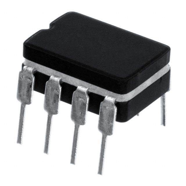
| 产品图片 |
|
| rohs | 符合RoHS无铅 / 符合限制有害物质指令(RoHS)规范要求 |
| 产品系列 | 接口 IC,RS-232接口集成电路,Texas Instruments SN65C3243DBR- |
| 数据手册 | |
| 产品型号 | SN65C3243DBR |
| 产品目录页面 | |
| 产品种类 | RS-232接口集成电路 |
| 供应商器件封装 | 28-SSOP |
| 其它名称 | 296-13120-6 |
| 功能 | Transceiver |
| 包装 | Digi-Reel® |
| 协议 | RS232 |
| 单位重量 | 208.400 mg |
| 双工 | 全 |
| 商标 | Texas Instruments |
| 安装类型 | 表面贴装 |
| 安装风格 | SMD/SMT |
| 封装 | Reel |
| 封装/外壳 | 28-SSOP(0.209",5.30mm 宽) |
| 封装/箱体 | SSOP-28 |
| 工作温度 | -40°C ~ 85°C |
| 工作温度范围 | - 40 C to + 85 C |
| 工作电源电压 | 3.3 V, 5 V |
| 工厂包装数量 | 2000 |
| 接收器滞后 | 500mV |
| 接收机数量 | 5 Receiver |
| 数据速率 | 1Mbps |
| 最大工作温度 | + 85 C |
| 最小工作温度 | - 40 C |
| 标准包装 | 1 |
| 激励器数量 | 3 Driver |
| 电压-电源 | 3 V ~ 5.5 V |
| 电源电流 | 1 mA |
| 类型 | 收发器 |
| 系列 | SN65C3243 |
| 驱动器/接收器数 | 3/5 |


- 商务部:美国ITC正式对集成电路等产品启动337调查
- 曝三星4nm工艺存在良率问题 高通将骁龙8 Gen1或转产台积电
- 太阳诱电将投资9.5亿元在常州建新厂生产MLCC 预计2023年完工
- 英特尔发布欧洲新工厂建设计划 深化IDM 2.0 战略
- 台积电先进制程称霸业界 有大客户加持明年业绩稳了
- 达到5530亿美元!SIA预计今年全球半导体销售额将创下新高
- 英特尔拟将自动驾驶子公司Mobileye上市 估值或超500亿美元
- 三星加码芯片和SET,合并消费电子和移动部门,撤换高东真等 CEO
- 三星电子宣布重大人事变动 还合并消费电子和移动部门
- 海关总署:前11个月进口集成电路产品价值2.52万亿元 增长14.8%


PDF Datasheet 数据手册内容提取
SN65C3243, SN75C3243 www.ti.com................................................................................................................................................. SLLS353H–JUNE1999–REVISEDSEPTEMBER2008 3-V TO 5.5-V MULTICHANNEL RS-232 COMPATIBLE LINE DRIVER/RECEIVER FEATURES 1 DB, DW, OR PW PACKAGE • OperatesWith3-Vto5.5-VV Supply CC (TOP VIEW) • Always-ActiveNoninvertingReceiverOutput (ROUT2B) C2+ 1 28 C1+ • LowStandbyCurrent...1m ATyp C2− 2 27 V+ • ExternalCapacitors...4×0.1m F V− 3 26 VCC RIN1 4 25 GND • Accepts5-VLogicInputWith3.3-VSupply RIN2 5 24 C1− • Inter-OperableWithSN65C3238,SN75C3238 RIN3 6 23 FORCEON • SupportsOperationFrom250kbit/sto RIN4 7 22 FORCEOFF 1Mbit/s RIN5 8 21 INVALID • RS-232Bus-PinESDProtectionExceeds DOUT1 9 20 ROUT2B ±15kVUsingHuman-BodyModel(HBM) DOUT2 10 19 ROUT1 • Latch-UpPerformanceExceeds100mAPer DOUT3 11 18 ROUT2 JESD78,ClassII DIN3 12 17 ROUT3 DIN2 13 16 ROUT4 APPLICATIONS DIN1 14 15 ROUT5 • Battery-PoweredSystems • PDAs • Notebooks • Laptops • PalmtopPCs • Hand-HeldEquipment DESCRIPTION/ORDERING INFORMATION The SN65C3243 and SN75C3243 consist of three line drivers, five line receivers, and a dual charge-pump circuit with ±15-kV ESD protection pin to pin (serial-port connection pins, including GND). This device provides the electricalinterface between an asynchronous communication controller and the serial-port connector. The charge pumpandfoursmallexternalcapacitorsallowoperationfromasingle3-Vto5.5-Vsupply.In addition, this device includes an always-active noninverting output (ROUT2B), which allows applications using the ring indicator to transmit data while the device is powered down. The device operates at data signaling rates up to 1 Mbit/s and anincreasedslew-raterangeof24V/m sto150V/m s. Flexible control options for power management are available when the serial port is inactive. The auto-powerdown feature functions when FORCEON is low and FORCEOFF is high. During this mode of operation, if the device does not sense a valid RS-232 signal, the driver outputs are disabled. If FORCEOFF is set low, both drivers and receivers (except ROUT2B) are shut off, and the supply current is reduced to 1 m A. Disconnectingtheserialportorturningofftheperipheraldriverscausestheauto-powerdownconditiontooccur. Auto-powerdown can be disabled when FORCEON and FORCEOFF are high and should be done when driving a serial mouse. With auto-powerdown enabled, the device is activated automatically when a valid signal is applied to any receiver input. The INVALID output is used to notify the user if an RS-232 signal is present at any receiver input. INVALID is high (valid data) if any receiver input voltage is greater than 2.7 V or less than –2.7 V or has been between –0.3 V and 0.3 V for less than 30 m s. INVALID is low (invalid data) if all receiver input voltagesarebetween–0.3Vand0.3Vformorethan30m s.RefertoFigure5forreceiverinputlevels. 1 Pleasebeawarethatanimportantnoticeconcerningavailability,standardwarranty,anduseincriticalapplicationsofTexas Instrumentssemiconductorproductsanddisclaimerstheretoappearsattheendofthisdatasheet. PRODUCTIONDATAinformationiscurrentasofpublicationdate. Copyright©1999–2008,TexasInstrumentsIncorporated Products conform to specifications per the terms of the Texas Instruments standard warranty. Production processing does not necessarilyincludetestingofallparameters.
SN65C3243, SN75C3243 SLLS353H–JUNE1999–REVISEDSEPTEMBER2008................................................................................................................................................. www.ti.com ORDERINGINFORMATION T PACKAGE(1)(2) ORDERABLEPARTNUMBER TOP-SIDEMARKING A Tubeof20 SN75C3243DW SOIC–DW 75C3243 Reelof1000 SN75C3243DWR 0°Cto70°C SSOP–DB Reelof2000 SN75C3243DBR 75C3243 Tubeof50 SN75C3243PW TSSOP–PW CA3243 Reelof2000 SN75C3243PWR Tubeof20 SN65C3243DW SOIC–DW 65C3243 Reelof1000 SN65C3243DWR –40°Cto85°C SSOP–DB Reelof2000 SN65C3243DBR 65C3243 Tubeof50 SN65C3243PW TSSOP–PW CB3243 Reelof2000 SN65C3243PWR (1) Packagedrawings,thermaldata,symbolizationareavailableatwww.ti.com/sc/packaging. (2) Forthemostcurrentpackageandorderinginformation,seethePackageOptionAddendumattheendofthisdocument,orseetheTI websiteatwww.ti.com. FUNCTION TABLES EACHDRIVER(1) INPUTS OUTPUT DIN FORCEON FORCEOFF VALIDRIN DOUT DRIVERSTATUS RS-232LEVEL X X L X Z Poweredoff L H H X H Normaloperationwithauto-powerdowndisabled H H H X L L L H Yes H Normaloperationwithauto-powerdownenabled H L H Yes L L L H No Z Poweredoffbyauto-powerdownfeature H L H No Z (1) H=highlevel,L=lowlevel,X=irrelevant,Z=highimpedance EACHRECEIVER(1) INPUTS OUTPUTS RIN1, VALIDRIN ROUT1, RECEIVERSTATUS RIN2 FORCEOFF RS-232 ROUT2B ROUT2 RIN3–RIN5 ROUT3–5 LEVEL L X L X L Z Z Poweredoffwhile H X L X H Z Z ROUT2Bisactive L L H YES L H H L H H YES L L L Normaloperationwith H L H YES H H H auto-powerdown disabled/enabled H H H YES H L L Open Open H YES L H H (1) H=highlevel,L=lowlevel,X=irrelevant,Z=highimpedance(off),Open=inputdisconnectedorconnecteddriveroff 2 SubmitDocumentationFeedback Copyright©1999–2008,TexasInstrumentsIncorporated ProductFolderLink(s):SN65C3243 SN75C3243
SN65C3243, SN75C3243 www.ti.com................................................................................................................................................. SLLS353H–JUNE1999–REVISEDSEPTEMBER2008 LOGICDIAGRAM(POSITIVELOGIC) 14 9 DIN1 DOUT1 13 10 DIN2 DOUT2 12 11 DIN3 DOUT3 22 FORCEOFF 21 Auto-Powerdown INVALID 23 FORCEON 19 4 ROUT1 RIN1 20 ROUT2B 18 5 ROUT2 RIN2 17 6 ROUT3 RIN3 16 7 ROUT4 RIN4 15 8 ROUT5 RIN5 Copyright©1999–2008,TexasInstrumentsIncorporated SubmitDocumentationFeedback 3 ProductFolderLink(s):SN65C3243 SN75C3243
SN65C3243, SN75C3243 SLLS353H–JUNE1999–REVISEDSEPTEMBER2008................................................................................................................................................. www.ti.com ABSOLUTE MAXIMUM RATINGS(1) overoperatingfree-airtemperaturerange(unlessotherwisenoted) MIN MAX UNIT V Supplyvoltagerange(2) –0.3 6 V CC V+ Positive-outputsupplyvoltagerange(2) –0.3 7 V V– Negative-outputsupplyvoltagerange(2) 0.3 –7 V V+–V– Supplyvoltagedifference(2) 13 V Driver(FORCEOFF,FORCEON) –0.3 6 V Inputvoltagerange V I Receiver –25 25 V Outputvoltagerange Driver –13.2 13.2 V O DBpackage 62 q Packagethermalimpedance(3)(4) DWpackage 46 °C/W JA PWpackage 62 T Operatingvirtualjunctiontemperature 150 °C J T Storagetemperaturerange –65 150 °C stg (1) Stressesbeyondthoselistedunder"absolutemaximumratings"maycausepermanentdamagetothedevice.Thesearestressratings only,andfunctionaloperationofthedeviceattheseoranyotherconditionsbeyondthoseindicatedunder"recommendedoperating conditions"isnotimplied.Exposuretoabsolute-maximum-ratedconditionsforextendedperiodsmayaffectdevicereliability. (2) AllvoltagesarewithrespecttonetworkGND. (3) MaximumpowerdissipationisafunctionofT(max),q ,andT .Themaximumallowablepowerdissipationatanyallowableambient J JA A temperatureisP =(T(max)–T )/q .OperatingattheabsolutemaximumT of150°Ccanaffectreliability. D J A JA J (4) ThepackagethermalimpedanceiscalculatedinaccordancewithJESD51-7. RECOMMENDED OPERATING CONDITIONS(1) seeFigure6 MIN NOM MAX UNIT V =3.3V 3 3.3 3.6 CC Supplyvoltage V V =5V 4.5 5 5.5 CC V =3.3V 2 CC V Driverandcontrolhigh-levelinputvoltage DIN,FORCEOFF,FORCEON V IH V =5V 2.4 CC V Driverandcontrollow-levelinputvoltage DIN,FORCEOFF,FORCEON 0.8 V IL V Driverandcontrolinputvoltage DIN,FORCEOFF,FORCEON 0 5.5 V I V Receiverinputvoltage –25 25 V I SN65C3243 –40 85 T Operatingfree-airtemperature °C A SN75C3243 0 70 (1) TestconditionsareC1–C4=0.1m FatV =3.3V±0.3V;C1=0.047m F,C2–C4=0.33m FatV =5V±0.5V. CC CC ELECTRICAL CHARACTERISTICS(1) overrecommendedrangesofsupplyvoltageandoperatingfree-airtemperature(unlessotherwisenoted)(seeFigure6) PARAMETER TESTCONDITIONS MIN TYP(2) MAX UNIT I Inputleakagecurrent FORCEOFF,FORCEON ±0.01 ±1 m A I Noload, Auto-powerdowndisabled 0.3 1 mA FORCEOFFandFORCEON=V CC Poweredoff Noload,FORCEOFF=GND 1 10 I Supplycurrent CC Noload,FORCEOFF=V , FORCEON=GND, CC m A Auto-powerdownenabled 1 10 AllRINareopenorgrounded, AllDINaregrounded (1) TestconditionsareC1–C4=0.1m FatV =3.3V±0.3V;C1=0.047m F,C2–C4=0.33m FatV =5V±0.5V. CC CC (2) AlltypicalvaluesareatV =3.3VorV =5V,andT =25°C. CC CC A 4 SubmitDocumentationFeedback Copyright©1999–2008,TexasInstrumentsIncorporated ProductFolderLink(s):SN65C3243 SN75C3243
SN65C3243, SN75C3243 www.ti.com................................................................................................................................................. SLLS353H–JUNE1999–REVISEDSEPTEMBER2008 DRIVER SECTION Electrical Characteristics(1) overrecommendedrangesofsupplyvoltageandoperatingfree-airtemperature(unlessotherwisenoted)(seeFigure6) PARAMETER TESTCONDITIONS MIN TYP(2) MAX UNIT High-leveloutput V AllDOUTatR =3kΩtoGND 5 5.4 V OH voltage L Low-leveloutput V AllDOUTatR =3kΩtoGND –5 –5.4 V OL voltage L Outputvoltage DIN1=DIN2=GND,DIN3=V ,3-kΩtoGNDatDOUT3, V CC ±5 V O (mousedriveability) DOUT1=DOUT2=2.5mA I High-levelinputcurrent V =V ±0.01 ±1 m A IH I CC I Low-levelinputcurrent V =GND ±0.01 ±1 m A IL I Short-circuitoutput VCC=3.6V, VO=0V ±35 ±60 IOS current(3) V =5.5V, V =0V ±35 ±90 mA CC O r Outputresistance V ,V+,andV–=0V, V =±2V 300 10M Ω o CC O V =±12V, V =3Vto3.6V ±25 I Outputleakagecurrent FORCEOFF=GND O CC m A off V =±10V, V =4.5Vto5.5V ±25 O CC (1) TestconditionsareC1–C4=0.1m FatV =3.3V±0.3V;C1=0.047m F,C2–C4=0.33m FatV =5V±0.5V. CC CC (2) AlltypicalvaluesareatV =3.3VorV =5V,andT =25°C. CC CC A (3) Short-circuitdurationsshouldbecontrolledtopreventexceedingthedeviceabsolutepowerdissipationratings,andnotmorethanone outputshouldbeshortedatatime. Switching Characteristics(1) overrecommendedrangesofsupplyvoltageandoperatingfree-airtemperature(unlessotherwisenoted)(seeFigure6) PARAMETER TESTCONDITIONS MIN TYP(2) MAX UNIT C =1000pF 250 L Maximumdatarate R =3kΩ, L C =250pF, V =3Vto4.5V 1000 kbit/s (seeFigure1) OneDOUTswitching L CC C =1000pF, V =4.5Vto5.5V 1000 L CC t Pulseskew(3) C =150pFto2500pF, R =3kΩto7kΩ, SeeFigure2 25 ns sk(p) L L Slewrate, SR(tr) transitionregion C =150pFto1000pF, R =3kΩto7kΩ, V =3.3V 18 150 V/m s L L CC (seeFigure1) (1) TestconditionsareC1–C4=0.1m FatV =3.3V±0.3V;C1=0.047m F,C2–C4=0.33m FatV =5V±0.5V. CC CC (2) AlltypicalvaluesareatV =3.3VorV =5V,andT =25°C. CC CC A (3) Pulseskewisdefinedas|t –t |ofeachchannelofthesamedevice. PLH PHL Copyright©1999–2008,TexasInstrumentsIncorporated SubmitDocumentationFeedback 5 ProductFolderLink(s):SN65C3243 SN75C3243
SN65C3243, SN75C3243 SLLS353H–JUNE1999–REVISEDSEPTEMBER2008................................................................................................................................................. www.ti.com RECEIVER SECTION Electrical Characteristics(1) overrecommendedrangesofsupplyvoltageandoperatingfree-airtemperature(unlessotherwisenoted)(seeFigure6) PARAMETER TESTCONDITIONS MIN TYP(2) MAX UNIT V High-leveloutputvoltage I =–1mA V –0.6 V –0.1 V OH OH CC CC V Low-leveloutputvoltage I =1.6mA 0.4 V OL OL V =3.3V 1.6 2.4 CC V Positive-goinginputthresholdvoltage V IT+ V =5V 1.9 2.4 CC V =3.3V 0.6 1.1 CC V Negative-goinginputthresholdvoltage V IT– V =5V 0.8 1.4 CC V Inputhysteresis(V –V ) 0.5 V hys IT+ IT– I Outputleakagecurrent(exceptROUT2B) FORCEOFF=0V ±0.05 ±10 m A off r Inputresistance V =±3Vto±25V 3 5 7 kΩ i I (1) TestconditionsareC1–C4=0.1m FatV =3.3V±0.3V;C1=0.047m F,C2–C4=0.33m FatV =5V±0.5V. CC CC (2) AlltypicalvaluesareatV =3.3VorV =5V,andT =25°C. CC CC A Switching Characteristics(1) overrecommendedrangesofsupplyvoltageandoperatingfree-airtemperature(unlessotherwisenoted) PARAMETER TESTCONDITIONS TYP(2) UNIT t Propagationdelaytime,low-tohigh-leveloutput C =150pF,SeeFigure3 150 ns PLH L t Propagationdelaytime,high-tolow-leveloutput C =150pF,SeeFigure3 150 ns PHL L t Outputenabletime C =150pF,R =3kΩ,SeeFigure4 200 ns en L L t Outputdisabletime C =150pF,R =3kΩ,SeeFigure4 200 ns dis L L t Pulseskew(3) SeeFigure3 50 ns sk(p) (1) TestconditionsareC1–C4=0.1m FatV =3.3V±0.3V;C1=0.047m F,C2–C4=0.33m FatV =5V±0.5V. CC CC (2) AlltypicalvaluesareatV =3.3VorV =5V,andT =25°C. CC CC A (3) Pulseskewisdefinedas|t –t |ofeachchannelofthesamedevice. PLH PHL 6 SubmitDocumentationFeedback Copyright©1999–2008,TexasInstrumentsIncorporated ProductFolderLink(s):SN65C3243 SN75C3243
SN65C3243, SN75C3243 www.ti.com................................................................................................................................................. SLLS353H–JUNE1999–REVISEDSEPTEMBER2008 AUTO-POWERDOWN SECTION Electrical Characteristics overrecommendedrangesofsupplyvoltageandoperatingfree-airtemperature(unlessotherwisenoted)(seeFigure5) PARAMETER TESTCONDITIONS MIN MAX UNIT Receiverinputthreshold V FORCEON=GND,FORCEOFF=V 2.7 V T+(valid) forINVALIDhigh-leveloutputvoltage CC Receiverinputthreshold V FORCEON=GND,FORCEOFF=V –2.7 V T–(valid) forINVALIDhigh-leveloutputvoltage CC Receiverinputthreshold V FORCEON=GND,FORCEOFF=V –0.3 0.3 V T(invalid) forINVALIDlow-leveloutputvoltage CC I =–1mA,FORCEON=GND, V INVALIDhigh-leveloutputvoltage OH V –0.6 V OH FORCEOFF=V CC CC I =1.6mA,FORCEON=GND, V INVALIDlow-leveloutputvoltage OL 0.4 V OL FORCEOFF=V CC Switching Characteristics overrecommendedrangesofsupplyvoltageandoperatingfree-airtemperature(unlessotherwisenoted)(seeFigure5) PARAMETER TYP(1) UNIT t Propagationdelaytime,low-tohigh-leveloutput 1 m s valid t Propagationdelaytime,high-tolow-leveloutput 30 m s invalid t Supplyenabletime 100 m s en (1) AlltypicalvaluesareatV =3.3VorV =5V,andT =25°C. CC CC A Copyright©1999–2008,TexasInstrumentsIncorporated SubmitDocumentationFeedback 7 ProductFolderLink(s):SN65C3243 SN75C3243
SN65C3243, SN75C3243 SLLS353H–JUNE1999–REVISEDSEPTEMBER2008................................................................................................................................................. www.ti.com PARAMETER MEASUREMENT INFORMATION 3 V RS-232 Input Output 0 V Generator 50 W (see Note B) RL C(sLe e Note A) tTHL tTLH 3 V 3 V 3 V VOH Output FORCEOFF −3 V −3 V VOL SR(tr)(cid:1) 6V t ort TEST CIRCUIT THL TLH VOLTAGE WAVEFORMS NOTES: A. CL includes probe and jig capacitance. B. The pulse generator has the following characteristics: PRR = 1 Mbit/s, ZO = 50 W , 50% duty cycle, tr ≤ 10 ns, tf ≤ 10 ns. Figure1.DriverSlewRate 3 V RS-232 Input 1.5 V 1.5 V Output 0 V Generator 50 W (see Note B) RL C(sLe e Note A) tPHL tPLH VOH 3 V Output 50% 50% FORCEOFF VOL TEST CIRCUIT VOLTAGE WAVEFORMS NOTES: A. CL includes probe and jig capacitance. B. The pulse generator has the following characteristics: PRR = 1 Mbit/s, ZO = 50 W , 50% duty cycle, tr ≤ 10 ns, tf ≤ 10 ns. Figure2.DriverPulseSkew 3 V or 0 V 3 V FORCEON Input 1.5 V 1.5 V −3 V Output Generator 50 W tPHL tPLH (see Note B) CL (see Note A) 3 V VOH FORCEOFF Output 50% 50% VOL TEST CIRCUIT VOLTAGE WAVEFORMS NOTES: A. CL includes probe and jig capacitance. B. The pulse generator has the following characteristics: ZO = 50 W , 50% duty cycle, tr ≤ 10 ns, tf ≤ 10 ns. Figure3.ReceiverPropagationDelayTimes 8 SubmitDocumentationFeedback Copyright©1999–2008,TexasInstrumentsIncorporated ProductFolderLink(s):SN65C3243 SN75C3243
SN65C3243, SN75C3243 www.ti.com................................................................................................................................................. SLLS353H–JUNE1999–REVISEDSEPTEMBER2008 PARAMETER MEASUREMENT INFORMATION (continued) 3 V Input 1.5 V 1.5 V VCC GND 3 V or 0 V 0 V S1 FORCEON tPHZ tPZH RL (S1 at GND) (S1 at GND) ±3 V Output VOH Output 50% CL 0.3 V (see Note A) FORCEOFF tPLZ tPZL Generator (S1 at VCC) (S1 at VCC) 50 W (see Note B) 0.3 V Output 50% VOL TEST CIRCUIT VOLTAGE WAVEFORMS NOTES: A. CL includes probe and jig capacitance. B. The pulse generator has the following characteristics: ZO = 50 W , 50% duty cycle, tr ≤ 10 ns, tf ≤ 10 ns. C. tPLZ and tPHZ are the same as tdis. D. tPZL and tPZH are the same as ten. Figure4.ReceiverEnableandDisableTimes Copyright©1999–2008,TexasInstrumentsIncorporated SubmitDocumentationFeedback 9 ProductFolderLink(s):SN65C3243 SN75C3243
SN65C3243, SN75C3243 SLLS353H–JUNE1999–REVISEDSEPTEMBER2008................................................................................................................................................. www.ti.com PARAMETER MEASUREMENT INFORMATION (continued) 3 V 2.7 V 2.7 V Receiver 0 V Input 0 V ROUT −2.7 V −2.7 V −3 V Generator 50 W (see Note B) tinvalid tvalid VCC 50% VCC 50% VCC INVALID 0 V Output Auto- INVALID ten powerdown V+ ≈V+ CL = 30 pF (see Note A) 0.3 V Supply VCC FORCEOFF Voltages 0 V 0.3 V DIN DOUT FORCEON V− ≈V− TEST CIRCUIT VOLTAGE WAVEFORMS ÎÎÎÎÎÎÎÎÎÎÎ Valid RS-232 Level, INVALID High ÎÎÎÎÎÎÎÎÎÎÎ 2.7 V ÎÎÎÎÎÎÎÎÎÎÎ Indeterminate ÎÎÎÎÎÎÎÎÎÎÎ 0.3 V ÎÎIfÎÎ SigÎÎnal RÎÎemÎÎainsÎÎ WitÎÎhin TÎÎhis ÎÎRegÎÎionÎÎ 0 V for More Than 30 m s, INVALID Is Low† ÎÎÎÎÎÎÎÎÎÎÎ −0.3 V ÎÎÎÎIndÎeteÎrminÎateÎÎÎÎ −2.7 VÎÎÎÎÎÎÎÎÎÎÎ ÎÎVaÎlid RÎS-23Î2 LeÎvel,Î INVÎALIDÎ HigÎh Î †Auto-powerdown disables drivers and reduces supply current to 1 m A. NOTES: A. CL includes probe and jig capacitance. B. The pulse generator has the following characteristics: PRR = 5 kbit/s, ZO = 50 W , 50% duty cycle, tr ≤ 10 ns, tf ≤ 10 ns. Figure5.INVALIDPropagationDelayTimesandSupplyEnablingTime 10 SubmitDocumentationFeedback Copyright©1999–2008,TexasInstrumentsIncorporated ProductFolderLink(s):SN65C3243 SN75C3243
SN65C3243, SN75C3243 www.ti.com................................................................................................................................................. SLLS353H–JUNE1999–REVISEDSEPTEMBER2008 PARAMETER MEASUREMENT INFORMATION (continued) 28 C1+ 27 1 V+ + C2+ + C3† C2 − 2 C2− 26 − +C1 VCC + CBYPASS − 3 V− 25 − = 0.1 m F − GND C4 + 24 C1− 4 23 RIN1 FORCEON 5 RIN2 n w Serial-Port Inputs RIN3 6 o-do 22 uter FORCEOFF 7 Aw RIN4 o P 8 RIN5 21 INVALID 9 20 DOUT1 ROUT2B 10 19 DOUT2 ROUT1 Serial-Port Outputs 5 kW 11 18 DOUT3 ROUT2 5 kW Logic Outputs 12 17 DIN3 ROUT3 5 kW 13 16 Logic Inputs DIN2 ROUT4 5 kW 14 15 DIN1 ROUT5 5 kW †C3 can be connected to VCC or GND. NOTE A: Resistor values shown are nominal. VCC vs CAPACITOR VALUES VCC C1 C2, C3, and C4 3.3 V ± 0.3 V 0.1 m F 0.1 m F 5 V ± 0.5 V 0.047 m F 0.33 m F 3 V to 5.5 V 0.1 m F 0.47 m F Figure6.TypicalOperatingCircuitandCapacitorValues Copyright©1999–2008,TexasInstrumentsIncorporated SubmitDocumentationFeedback 11 ProductFolderLink(s):SN65C3243 SN75C3243
PACKAGE OPTION ADDENDUM www.ti.com 6-Feb-2020 PACKAGING INFORMATION Orderable Device Status Package Type Package Pins Package Eco Plan Lead/Ball Finish MSL Peak Temp Op Temp (°C) Device Marking Samples (1) Drawing Qty (2) (6) (3) (4/5) SN65C3243DBR ACTIVE SSOP DB 28 2000 Green (RoHS NIPDAU Level-1-260C-UNLIM -40 to 85 65C3243 & no Sb/Br) SN65C3243DBRG4 ACTIVE SSOP DB 28 2000 Green (RoHS NIPDAU Level-1-260C-UNLIM -40 to 85 65C3243 & no Sb/Br) SN65C3243DW ACTIVE SOIC DW 28 20 Green (RoHS NIPDAU Level-1-260C-UNLIM -40 to 85 65C3243 & no Sb/Br) SN65C3243DWR ACTIVE SOIC DW 28 1000 Green (RoHS NIPDAU Level-1-260C-UNLIM -40 to 85 65C3243 & no Sb/Br) SN65C3243PW ACTIVE TSSOP PW 28 50 Green (RoHS NIPDAU Level-1-260C-UNLIM -40 to 85 CB3243 & no Sb/Br) SN65C3243PWR ACTIVE TSSOP PW 28 2000 Green (RoHS NIPDAU Level-1-260C-UNLIM -40 to 85 CB3243 & no Sb/Br) SN75C3243DBR ACTIVE SSOP DB 28 2000 Green (RoHS NIPDAU Level-1-260C-UNLIM 0 to 70 75C3243 & no Sb/Br) SN75C3243DW ACTIVE SOIC DW 28 20 Green (RoHS NIPDAU Level-1-260C-UNLIM 0 to 70 75C3243 & no Sb/Br) SN75C3243DWR ACTIVE SOIC DW 28 1000 Green (RoHS NIPDAU Level-1-260C-UNLIM 0 to 70 75C3243 & no Sb/Br) SN75C3243PW ACTIVE TSSOP PW 28 50 Green (RoHS NIPDAU Level-1-260C-UNLIM 0 to 70 CA3243 & no Sb/Br) SN75C3243PWR ACTIVE TSSOP PW 28 2000 Green (RoHS NIPDAU Level-1-260C-UNLIM 0 to 70 CA3243 & no Sb/Br) (1) The marketing status values are defined as follows: ACTIVE: Product device recommended for new designs. LIFEBUY: TI has announced that the device will be discontinued, and a lifetime-buy period is in effect. NRND: Not recommended for new designs. Device is in production to support existing customers, but TI does not recommend using this part in a new design. PREVIEW: Device has been announced but is not in production. Samples may or may not be available. OBSOLETE: TI has discontinued the production of the device. (2) RoHS: TI defines "RoHS" to mean semiconductor products that are compliant with the current EU RoHS requirements for all 10 RoHS substances, including the requirement that RoHS substance do not exceed 0.1% by weight in homogeneous materials. Where designed to be soldered at high temperatures, "RoHS" products are suitable for use in specified lead-free processes. TI may reference these types of products as "Pb-Free". RoHS Exempt: TI defines "RoHS Exempt" to mean products that contain lead but are compliant with EU RoHS pursuant to a specific EU RoHS exemption. Green: TI defines "Green" to mean the content of Chlorine (Cl) and Bromine (Br) based flame retardants meet JS709B low halogen requirements of <=1000ppm threshold. Antimony trioxide based flame retardants must also meet the <=1000ppm threshold requirement. Addendum-Page 1
PACKAGE OPTION ADDENDUM www.ti.com 6-Feb-2020 (3) MSL, Peak Temp. - The Moisture Sensitivity Level rating according to the JEDEC industry standard classifications, and peak solder temperature. (4) There may be additional marking, which relates to the logo, the lot trace code information, or the environmental category on the device. (5) Multiple Device Markings will be inside parentheses. Only one Device Marking contained in parentheses and separated by a "~" will appear on a device. If a line is indented then it is a continuation of the previous line and the two combined represent the entire Device Marking for that device. (6) Lead/Ball Finish - Orderable Devices may have multiple material finish options. Finish options are separated by a vertical ruled line. Lead/Ball Finish values may wrap to two lines if the finish value exceeds the maximum column width. Important Information and Disclaimer:The information provided on this page represents TI's knowledge and belief as of the date that it is provided. TI bases its knowledge and belief on information provided by third parties, and makes no representation or warranty as to the accuracy of such information. Efforts are underway to better integrate information from third parties. TI has taken and continues to take reasonable steps to provide representative and accurate information but may not have conducted destructive testing or chemical analysis on incoming materials and chemicals. TI and TI suppliers consider certain information to be proprietary, and thus CAS numbers and other limited information may not be available for release. In no event shall TI's liability arising out of such information exceed the total purchase price of the TI part(s) at issue in this document sold by TI to Customer on an annual basis. Addendum-Page 2
PACKAGE MATERIALS INFORMATION www.ti.com 11-Jun-2020 TAPE AND REEL INFORMATION *Alldimensionsarenominal Device Package Package Pins SPQ Reel Reel A0 B0 K0 P1 W Pin1 Type Drawing Diameter Width (mm) (mm) (mm) (mm) (mm) Quadrant (mm) W1(mm) SN65C3243DBR SSOP DB 28 2000 330.0 16.4 8.2 10.5 2.5 12.0 16.0 Q1 SN65C3243DWR SOIC DW 28 1000 330.0 32.4 11.35 18.67 3.1 16.0 32.0 Q1 SN65C3243PWR TSSOP PW 28 2000 330.0 16.4 6.9 10.2 1.8 12.0 16.0 Q1 SN65C3243PWR TSSOP PW 28 2000 330.0 16.4 6.9 10.2 1.8 12.0 16.0 Q1 SN75C3243DBR SSOP DB 28 2000 330.0 16.4 8.2 10.5 2.5 12.0 16.0 Q1 SN75C3243DWR SOIC DW 28 1000 330.0 32.4 11.35 18.67 3.1 16.0 32.0 Q1 SN75C3243PWR TSSOP PW 28 2000 330.0 16.4 6.9 10.2 1.8 12.0 16.0 Q1 PackMaterials-Page1
PACKAGE MATERIALS INFORMATION www.ti.com 11-Jun-2020 *Alldimensionsarenominal Device PackageType PackageDrawing Pins SPQ Length(mm) Width(mm) Height(mm) SN65C3243DBR SSOP DB 28 2000 367.0 367.0 38.0 SN65C3243DWR SOIC DW 28 1000 350.0 350.0 66.0 SN65C3243PWR TSSOP PW 28 2000 367.0 367.0 38.0 SN65C3243PWR TSSOP PW 28 2000 350.0 350.0 43.0 SN75C3243DBR SSOP DB 28 2000 367.0 367.0 38.0 SN75C3243DWR SOIC DW 28 1000 350.0 350.0 66.0 SN75C3243PWR TSSOP PW 28 2000 367.0 367.0 38.0 PackMaterials-Page2
PACKAGE OUTLINE DB0028A SSOP - 2 mm max height SCALE 1.500 SMALL OUTLINE PACKAGE C 8.2 TYP 7.4 A 0.1 C PIN 1 INDEX AREA SEATING PLANE 26X 0.65 28 1 2X 10.5 8.45 9.9 NOTE 3 14 15 0.38 28X 0.22 5.6 0.15 C A B B 5.0 NOTE 4 2 MAX 0.25 (0.15) TYP SEE DETAIL A GAGE PLANE 0 -8 0.95 0.05 MIN 0.55 DETA 15AIL A TYPICAL 4214853/B 03/2018 NOTES: 1. All linear dimensions are in millimeters. Any dimensions in parenthesis are for reference only. Dimensioning and tolerancing per ASME Y14.5M. 2. This drawing is subject to change without notice. 3. This dimension does not include mold flash, protrusions, or gate burrs. Mold flash, protrusions, or gate burrs shall not exceed 0.15 mm per side. 4. This dimension does not include interlead flash. Interlead flash shall not exceed 0.25 mm per side. 5. Reference JEDEC registration MO-150. www.ti.com
EXAMPLE BOARD LAYOUT DB0028A SSOP - 2 mm max height SMALL OUTLINE PACKAGE 28X (1.85) SYMM (R0.05) TYP 1 28X (0.45) 28 26X (0.65) SYMM 14 15 (7) LAND PATTERN EXAMPLE EXPOSED METAL SHOWN SCALE: 10X SOLDER MASK METAL METAL UNDER SOLDER MASK OPENING SOLDER MASK OPENING EXPOSED METAL EXPOSED METAL 0.07 MAX 0.07 MIN ALL AROUND ALL AROUND NON-SOLDER MASK SOLDER MASK DEFINED DEFINED (PREFERRED) SOLDE15.000 R MASK DETAILS 4214853/B 03/2018 NOTES: (continued) 6. Publication IPC-7351 may have alternate designs. 7. Solder mask tolerances between and around signal pads can vary based on board fabrication site. www.ti.com
EXAMPLE STENCIL DESIGN DB0028A SSOP - 2 mm max height SMALL OUTLINE PACKAGE 28X (1.85) SYMM (R0.05) TYP 1 28X (0.45) 28 26X (0.65) SYMM 14 15 (7) SOLDER PASTE EXAMPLE BASED ON 0.125 mm THICK STENCIL SCALE: 10X 4214853/B 03/2018 NOTES: (continued) 8. Laser cutting apertures with trapezoidal walls and rounded corners may offer better paste release. IPC-7525 may have alternate design recommendations. 9. Board assembly site may have different recommendations for stencil design. www.ti.com
None
None
None
None
IMPORTANTNOTICEANDDISCLAIMER TI PROVIDES TECHNICAL AND RELIABILITY DATA (INCLUDING DATASHEETS), DESIGN RESOURCES (INCLUDING REFERENCE DESIGNS), APPLICATION OR OTHER DESIGN ADVICE, WEB TOOLS, SAFETY INFORMATION, AND OTHER RESOURCES “AS IS” AND WITH ALL FAULTS, AND DISCLAIMS ALL WARRANTIES, EXPRESS AND IMPLIED, INCLUDING WITHOUT LIMITATION ANY IMPLIED WARRANTIES OF MERCHANTABILITY, FITNESS FOR A PARTICULAR PURPOSE OR NON-INFRINGEMENT OF THIRD PARTY INTELLECTUAL PROPERTY RIGHTS. These resources are intended for skilled developers designing with TI products. You are solely responsible for (1) selecting the appropriate TI products for your application, (2) designing, validating and testing your application, and (3) ensuring your application meets applicable standards, and any other safety, security, or other requirements. These resources are subject to change without notice. TI grants you permission to use these resources only for development of an application that uses the TI products described in the resource. Other reproduction and display of these resources is prohibited. No license is granted to any other TI intellectual property right or to any third party intellectual property right. TI disclaims responsibility for, and you will fully indemnify TI and its representatives against, any claims, damages, costs, losses, and liabilities arising out of your use of these resources. TI’s products are provided subject to TI’s Terms of Sale (www.ti.com/legal/termsofsale.html) or other applicable terms available either on ti.com or provided in conjunction with such TI products. TI’s provision of these resources does not expand or otherwise alter TI’s applicable warranties or warranty disclaimers for TI products. Mailing Address: Texas Instruments, Post Office Box 655303, Dallas, Texas 75265 Copyright © 2020, Texas Instruments Incorporated