 Datasheet下载
- 型号: SMS12CT1G
- 制造商: ON Semiconductor
- 库位|库存: xxxx|xxxx
- 要求:
| 数量阶梯 | 香港交货 | 国内含税 |
| +xxxx | $xxxx | ¥xxxx |
查看当月历史价格
查看今年历史价格
SMS12CT1G产品简介:
ICGOO电子元器件商城为您提供SMS12CT1G由ON Semiconductor设计生产,在icgoo商城现货销售,并且可以通过原厂、代理商等渠道进行代购。 SMS12CT1G价格参考。ON SemiconductorSMS12CT1G封装/规格:TVS - 二极管, 。您可以下载SMS12CT1G参考资料、Datasheet数据手册功能说明书,资料中有SMS12CT1G 详细功能的应用电路图电压和使用方法及教程。
SMS12CT1G是ON Semiconductor(现为安森美半导体)生产的TVS(瞬态电压抑制器)二极管。这类器件主要用于保护电子电路免受瞬态电压的损害,如静电放电(ESD)、电快速瞬变脉冲群(EFT)和雷击感应浪涌等。

 应用场景

1. 消费电子产品:
   - 智能手机和平板电脑:用于保护USB接口、耳机插孔、充电接口等敏感电路。
   - 笔记本电脑:保护电源接口、数据传输接口(如HDMI、DisplayPort)以及Wi-Fi模块等。
   - 智能家居设备:如智能音箱、智能灯泡等,保护其通信接口(如Zigbee、蓝牙、Wi-Fi)和电源输入端。

2. 汽车电子:
   - 车载信息娱乐系统:保护音频、视频输入输出接口,防止因外部设备连接时产生的瞬态电压损坏系统。
   - 传感器模块:如倒车雷达、摄像头等,保护其信号传输线路。
   - 车载网络通信:如CAN总线、LIN总线等,确保通信稳定性和可靠性。

3. 工业控制:
   - 可编程逻辑控制器(PLC):保护输入输出端口,防止因外部干扰或误操作导致的损坏。
   - 传感器和执行器:保护模拟信号和数字信号传输线路,确保数据的准确性和稳定性。
   - 工业通信接口:如RS-485、RS-232等,防止外界电磁干扰和瞬态电压对通信的影响。

4. 通信设备:
   - 路由器和交换机:保护以太网端口、光纤接口等,确保网络通信的可靠性和稳定性。
   - 基站设备:保护射频前端、电源输入端等关键部位,防止雷击和其他瞬态电压的损害。

5. 医疗设备:
   - 便携式医疗设备:如血糖仪、血压计等,保护其电源和通信接口,确保测量结果的准确性。
   - 大型医疗设备:如X光机、CT扫描仪等,保护其复杂的内部电路,确保设备的安全性和可靠性。

总之,SMS12CT1G作为一种高效的瞬态电压抑制器,广泛应用于各种需要高可靠性和高防护等级的电子设备中,确保这些设备在复杂电磁环境下能够正常工作并延长使用寿命。
| 参数 | 数值 |
| 产品目录 | |
| 描述 | TVS DIODE 12VWM 23VC SC746TVS二极管阵列 5 Line TVS Array |
| 产品分类 | |
| 品牌 | ON Semiconductor |
| 产品手册 | |
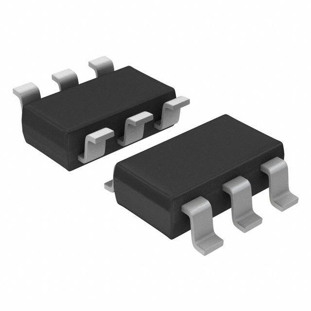
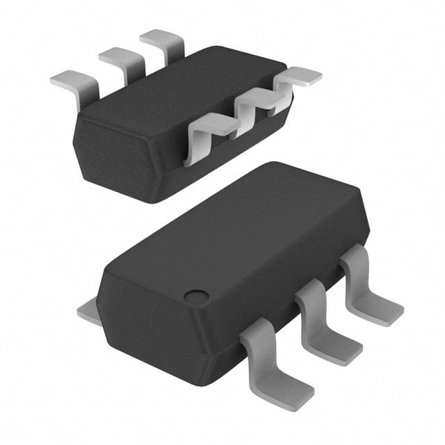
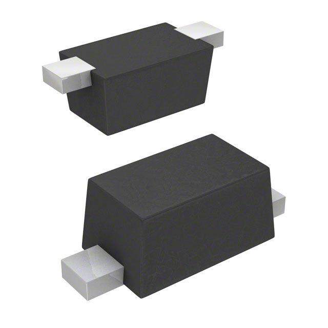
| 产品图片 |
|
| rohs | 符合RoHS无铅 / 符合限制有害物质指令(RoHS)规范要求 |
| 产品系列 | 二极管与整流器,TVS二极管,TVS二极管阵列,ON Semiconductor SMS12CT1G- |
| 数据手册 | |
| 产品型号 | SMS12CT1G |
| 不同频率时的电容 | 120pF @ 1MHz |
| 产品种类 | TVS二极管阵列 |
| 供应商器件封装 | 6-TSOP |
| 其它名称 | SMS12CT1GOS |
| 击穿电压 | 13.3 V |
| 功率-峰值脉冲 | 350W |
| 包装 | 带卷 (TR) |
| 单向通道 | 5 |
| 双向通道 | - |
| 商标 | ON Semiconductor |
| 安装类型 | 表面贴装 |
| 安装风格 | SMD/SMT |
| 封装 | Reel |
| 封装/外壳 | SC-74,SOT-457 |
| 封装/箱体 | TSOP-6 |
| 尺寸 | 1.5 mm W x 3 mm L |
| 峰值浪涌电流 | 15 A |
| 峰值脉冲功率耗散 | 350 W |
| 工作温度 | -40°C ~ 125°C (TJ) |
| 工作电压 | 12 V |
| 工厂包装数量 | 3000 |
| 应用 | 通用 |
| 最大工作温度 | + 125 C |
| 最小工作温度 | - 40 C |
| 极性 | Unidirectional |
| 标准包装 | 3,000 |
| 电压-击穿(最小值) | 13.3V |
| 电压-反向关态(典型值) | 12V (最小值) |
| 电压-箝位(最大值)@Ipp | 23V |
| 电容 | 120 pF |
| 电流-峰值脉冲(10/1000µs) | 15A (8/20µs) |
| 电源线路保护 | 无 |
| 端接类型 | SMD/SMT |
| 类型 | 齐纳 |
| 系列 | SMSxxC |
| 通道 | 5 Channels |
| 钳位电压 | 23 V |


- 商务部:美国ITC正式对集成电路等产品启动337调查
- 曝三星4nm工艺存在良率问题 高通将骁龙8 Gen1或转产台积电
- 太阳诱电将投资9.5亿元在常州建新厂生产MLCC 预计2023年完工
- 英特尔发布欧洲新工厂建设计划 深化IDM 2.0 战略
- 台积电先进制程称霸业界 有大客户加持明年业绩稳了
- 达到5530亿美元!SIA预计今年全球半导体销售额将创下新高
- 英特尔拟将自动驾驶子公司Mobileye上市 估值或超500亿美元
- 三星加码芯片和SET,合并消费电子和移动部门,撤换高东真等 CEO
- 三星电子宣布重大人事变动 还合并消费电子和移动部门
- 海关总署:前11个月进口集成电路产品价值2.52万亿元 增长14.8%


PDF Datasheet 数据手册内容提取
SMS05C, SMS12C, SMS15C, SMS24C ESD Protection Diode Array, 5-Line This 5−line surge protection array is designed for application requiring transient voltage protection capability. It is intended for use wwwwww..oonnsseemmii..ccoomm in over−transient voltage and ESD sensitive equipment such as computers, printers, automotive electronics, networking TSOP−6 FIVE SURGE communication and other applications. This device features a PROTECTION monolithic common anode design which protects five independent 350 W PEAK POWER lines in a single TSOP−6 package. PIN ASSIGNMENT Features • Protects up to 5 Lines in a Single TSOP−6 Package • Peak Power Dissipation − 350 W (8 (cid:2) 20 (cid:2)s Waveform) 1 6 • ESD Rating of Class 3B (Exceeding 8.0 kV) per Human Body Model 6 2 5 and Class C (Exceeding 400 V) per Machine Model • 1 3 4 Compliance with IEC 61000−4−2 (ESD) 15 kV (Air), 8.0 kV TSOP−6 (Contact) CASE 318G PIN 1.CATHODE • Flammability Rating of UL 94 V−0 SCALE 2:1 2.ANODE • 3.CATHODE These are Pb−Free Devices 4.CATHODE 5.CATHODE Applications 6.CATHODE • Hand−Held Portable Applications • MARKING DIAGRAM Networking and Telecom • Automotive Electronics • Serial and Parallel Ports 6x M(cid:2) • (cid:2) Notebooks, Desktops, Servers MAXIMUM RATINGS (TJ = 25°C unless otherwise specified) x = SMS05C:J Symbol Rating Value Unit = SMS12C:K = SMS15C:L PPK 1 Peak Power Dissipation 350 W = SMS24C:M 8 (cid:2) 20 (cid:2)s Double Exponential Waveform M = Date Code (Note 1) (cid:2) = Pb−Free Package T Operating Junction Temperature Range −40 to 150 °C (Note: Microdot may be in either location) J TSTG Storage Temperature Range −55 to 150 °C TL Lead Solder Temperature (10 s) 260 °C ORDERING INFORMATION ESD Human Body Model ( HBM) >8000 V Device Package Shipping† Machine Model (MM) >400 IEC 61000−4−2 Air (ESD) >15000 SMS05CT1G IEC 61000−4−2 Contact (ESD) >8000 Stresses exceeding those listed in the Maximum Ratings table may damage the SMS12CT1G TSOP−6 3000/Tape & Reel device. If any of these limits are exceeded, device functionality should not be (Pb−Free) SMS15CT1G assumed, damage may occur and reliability may be affected. 1. Non−repetitive current pulse per Figure 3. SMS24CT1G †For information on tape and reel specifications, including part orientation and tape sizes, please refer to our Tape and Reel Packaging Specification Brochure, BRD8011/D. © Semiconductor Components Industries, LLC, 2011 1 Publication Order Number: November, 2017 − Rev. 8 SMS05C/D
SMS05C, SMS12C, SMS15C, SMS24C SMS05C ELECTRICAL CHARACTERISTICS (TJ = 25°C unless otherwise specified) Parameter Symbol Conditions Min Typ Max Unit Reverse Working Voltage VRWM (Note 2) 5.0 V Breakdown Voltage VBR IT = 1.0 mA (Note 3) 6.2 7.2 V Reverse Leakage Current IR VRWM = 5.0 V 5.0 (cid:2)A Clamping Voltage VC IPP = 5.0 A (8 (cid:2) 20 (cid:2)s Waveform) 9.8 V Clamping Voltage VC IPP = 24 A (8 (cid:2) 20 (cid:2)s Waveform) 14.5 V Maximum Peak Pulse Current IPP 8 (cid:2) 20 (cid:2)s Waveform 24 A Capacitance CJ VR = 0 V, f = 1.0 MHz (Line to GND) 260 400 pF SMS12C ELECTRICAL CHARACTERISTICS (TJ = 25°C unless otherwise specified) Parameter Symbol Conditions Min Typ Max Unit Reverse Working Voltage VRWM (Note 2) 12 V Breakdown Voltage VBR IT = 1.0 mA (Note 3) 13.3 15 V Reverse Leakage Current IR VRWM = 12 V 0.001 1.0 (cid:2)A Clamping Voltage VC IPP = 5.0 A (8 (cid:2) 20 (cid:2)s Waveform) 19 V Clamping Voltage VC IPP = 15 A (8 (cid:2) 20 (cid:2)s Waveform) 23 V Maximum Peak Pulse Current IPP 8 (cid:2) 20 (cid:2)s Waveform 15 A Capacitance CJ VR = 0 V, f = 1.0 MHz (Line to GND) 120 150 pF SMS15C ELECTRICAL CHARACTERISTICS (TJ = 25°C, unless otherwise specified) (See Note 4) Parameter Symbol Conditions Min Typ Max Unit Reverse Working Voltage VRWM (Note 2) 15 V Breakdown Voltage VBR IT = 1.0 mA (Note 3) 17 19 V Reverse Leakage Current IR VRWM = 15 V 0.05 1.0 (cid:2)A Clamping Voltage VC IPP = 5.0 A (8 (cid:2) 20 (cid:2)s Waveform) 24 V Clamping Voltage VC IPP = 12 A (8 (cid:2) 20 (cid:2)s Waveform) 29 V Maximum Peak Pulse Current IPP 8 (cid:2) 20 (cid:2)s Waveform 12 A Capacitance CJ VR = 0 V, f = 1.0 MHz (Line to GND) 95 125 pF SMS24C ELECTRICAL CHARACTERISTICS (TJ = 25°C, unless otherwise specified) Parameter Symbol Conditions Min Typ Max Unit Reverse Working Voltage VRWM (Note 2) 24 V Breakdown Voltage VBR IT = 1.0 mA (Note 3) 26.7 32 V Reverse Leakage Current IR VRWM = 24 V 0.001 1.0 (cid:2)A Clamping Voltage VC IPP = 5.0 A (8 (cid:2) 20 (cid:2)s Waveform) 40 V Clamping Voltage VC IPP = 8 A (8 (cid:2) 20 (cid:2)s Waveform) 44 V Maximum Peak Pulse Current IPP 8 (cid:2) 20 (cid:2)s Waveform 8.0 A Capacitance CJ VR = 0 V, f = 1.0 MHz (Line to GND) 60 75 pF 2. Surge protection devices are normally selected according to the working peak reverse voltage (VRWM), which should be equal or greater than the DC or continuous peak operating voltage level. 3. VBR is measured at pulse test current IT. 4. Parametrics are the same for the Pb−Free packages, which are suffixed with a “G’’. www.onsemi.com 2
SMS05C, SMS12C, SMS15C, SMS24C TYPICAL PERFORMANCE CURVES (TJ = 25°C unless otherwise specified) OWER 19000 T19000 tr PEAK VALUE IRSM @ 8 (cid:2)s K P 80 EN 80 PULSE WIDTH (tP) IS DEFINED NG IN % OF PEA°C= 25NT @ TA 765000 PULSE CURR 765000 HAAPLSEF A TVKAH LACUTU ERP OIRREISNNMT/T2 W D@HE EC2R0A EY(cid:2) s=T H8E (cid:2)s E DERATIR CURRE 4300 F PEAK 4300 tP SO 20 O 20 UL % K P 10 10 A E 0 0 P 0 25 50 75 100 125 150 175 200 0 20 40 60 80 TA, AMBIENT TEMPERATURE (°C) t, TIME ((cid:2)s) Figure 1. Pulse Derating Curve Figure 2. 8 × 20 (cid:2)s Pulse Waveform 50 300 SMS24C 8 x 20 (cid:2)s f = 1.0 MHz V) 45 PULSE WAVEFORM pF)250 E ( 40 E ( G C A 35 N T SMS15C A200 VOL 30 SMS12C CIT SMS05C G 25 PA150 N A MPI 20 N C CLA 15 SMS05C CTIO100 , C 10 N SMS12C V U 50 5 J SMS15C SMS24C 0 0 0 5 10 15 20 25 0 5 10 15 20 25 IPP, PEAK PULSE CURRENT (A) VBR, REVERSE VOLTAGE (V) Figure 3. Clamping Voltage vs. Peak Pulse Current Figure 4. Junction Capacitance vs. Reverse Voltage Figure 5. ESD Pulse IEC 61000−4−2 Figure 6. SMS15CT1 ESD Response for IEC (8.0 kV Contact) 61000−4−2 (+8.0 kV Contact) www.onsemi.com 3
SMS05C, SMS12C, SMS15C, SMS24C TYPICAL COMMON ANODE APPLICATIONS A 5 surge protection junction common anode design in a especially when board space is at a premium. A simplified TSOP−6 package protects four separate lines using only one example of SMS05C Series Device applications is package. This adds flexibility and creativity to PCB design illustrated below. A KEYBOARD B TERMINAL FUNCTIONAL I/O C PRINTER DECODER D ETC. E GND SMS05C SERIES DEVICE Figure 7. Computer Interface Protection VDD VGG ADDRESS BUS RAM ROM DATA BUS CPU I/O CLOCK CONTROL BUS GND SMS05C SERIES DEVICE Figure 8. Microprocessor Protection www.onsemi.com 4
SMS05C, SMS12C, SMS15C, SMS24C PACKAGE DIMENSIONS TSOP−6 CASE 318G−02 ISSUE V D NOTES: 1. DIMENSIONING AND TOLERANCING PER ASME Y14.5M, 1994. H 2. CONTROLLING DIMENSION: MILLIMETERS. 3. MAXIMUM LEAD THICKNESS INCLUDES LEAD FINISH. MINIMUM LEAD THICKNESS IS THE MINIMUM THICKNESS OF BASE MATERIAL. É6 É5 4 L2 4. DIMENSIONS D AND E1 DO NOT INCLUDE MOLD FLASH, GAUGE PROTRUSIONS, OR GATE BURRS. MOLD FLASH, PROTRUSIONS, OR E1 E PLANE GATE BURRS SHALL NOT EXCEED 0.15 PER SIDE. DIMENSIONS D ÉÉ AND E1 ARE DETERMINED AT DATUM H. 1 2 3 5. PIN ONE INDICATOR MUST BE LOCATED IN THE INDICATED ZONE. L NOTE 5 b M C PSLEAANTIENG DIM MIN MILLNIMOEMTERSMAX DETAIL Z A 0.90 1.00 1.10 e A1 0.01 0.06 0.10 b 0.25 0.38 0.50 c 0.10 0.18 0.26 c D 2.90 3.00 3.10 0.05 A EE1 21..5300 21..7550 31..0700 e 0.85 0.95 1.05 A1 L 0.20 0.40 0.60 DETAIL Z L2 0.25 BSC M 0(cid:2) − 10(cid:2) RECOMMENDED SOLDERING FOOTPRINT* 6X 0.60 3.20 6X 0.95 0.95 PITCH DIMENSIONS: MILLIMETERS *For additional information on our Pb−Free strategy and soldering details, please download the ON Semiconductor Soldering and Mounting Techniques Reference Manual, SOLDERRM/D. ON Semiconductor and are trademarks of Semiconductor Components Industries, LLC dba ON Semiconductor or its subsidiaries in the United States and/or other countries. ON Semiconductor owns the rights to a number of patents, trademarks, copyrights, trade secrets, and other intellectual property. A listing of ON Semiconductor’s product/patent coverage may be accessed at www.onsemi.com/site/pdf/Patent−Marking.pdf. ON Semiconductor reserves the right to make changes without further notice to any products herein. ON Semiconductor makes no warranty, representation or guarantee regarding the suitability of its products for any particular purpose, nor does ON Semiconductor assume any liability arising out of the application or use of any product or circuit, and specifically disclaims any and all liability, including without limitation special, consequential or incidental damages. Buyer is responsible for its products and applications using ON Semiconductor products, including compliance with all laws, regulations and safety requirements or standards, regardless of any support or applications information provided by ON Semiconductor. “Typical” parameters which may be provided in ON Semiconductor data sheets and/or specifications can and do vary in different applications and actual performance may vary over time. All operating parameters, including “Typicals” must be validated for each customer application by customer’s technical experts. ON Semiconductor does not convey any license under its patent rights nor the rights of others. ON Semiconductor products are not designed, intended, or authorized for use as a critical component in life support systems or any FDA Class 3 medical devices or medical devices with a same or similar classification in a foreign jurisdiction or any devices intended for implantation in the human body. Should Buyer purchase or use ON Semiconductor products for any such unintended or unauthorized application, Buyer shall indemnify and hold ON Semiconductor and its officers, employees, subsidiaries, affiliates, and distributors harmless against all claims, costs, damages, and expenses, and reasonable attorney fees arising out of, directly or indirectly, any claim of personal injury or death associated with such unintended or unauthorized use, even if such claim alleges that ON Semiconductor was negligent regarding the design or manufacture of the part. ON Semiconductor is an Equal Opportunity/Affirmative Action Employer. This literature is subject to all applicable copyright laws and is not for resale in any manner. PUBLICATION ORDERING INFORMATION LITERATURE FULFILLMENT: N. American Technical Support: 800−282−9855 Toll Free ON Semiconductor Website: www.onsemi.com Literature Distribution Center for ON Semiconductor USA/Canada 19521 E. 32nd Pkwy, Aurora, Colorado 80011 USA Europe, Middle East and Africa Technical Support: Order Literature: http://www.onsemi.com/orderlit Phone: 303−675−2175 or 800−344−3860 Toll Free USA/Canada Phone: 421 33 790 2910 Fax: 303−675−2176 or 800−344−3867 Toll Free USA/Canada Japan Customer Focus Center For additional information, please contact your local Email: orderlit@onsemi.com Phone: 81−3−5817−1050 Sales Representative ◊ www.onsemi.com SMS05C/D 5
Mouser Electronics Authorized Distributor Click to View Pricing, Inventory, Delivery & Lifecycle Information: O N Semiconductor: SMS05CT1G SMS12CT1G SMS15CT1G SMS24CT1G