 Datasheet下载
- 型号: SMF51A
- 制造商: Littelfuse
- 库位|库存: xxxx|xxxx
- 要求:
| 数量阶梯 | 香港交货 | 国内含税 |
| +xxxx | $xxxx | ¥xxxx |
查看当月历史价格
查看今年历史价格
SMF51A产品简介:
ICGOO电子元器件商城为您提供SMF51A由Littelfuse设计生产,在icgoo商城现货销售,并且可以通过原厂、代理商等渠道进行代购。 SMF51A价格参考。LittelfuseSMF51A封装/规格:TVS - 二极管, 。您可以下载SMF51A参考资料、Datasheet数据手册功能说明书,资料中有SMF51A 详细功能的应用电路图电压和使用方法及教程。
Littelfuse Inc. 的SMF51A TVS二极管(瞬态电压抑制二极管)主要用于保护电子设备免受瞬态电压尖峰的损害。它具有快速响应时间、高浪涌电流承受能力以及低箝位电压等特点,适用于多种应用场景。

 1. 消费电子
   - 智能手机和平板电脑:在这些便携式设备中,SMF51A可以保护电源线和数据接口(如USB、HDMI等)免受静电放电(ESD)和雷击引起的电压浪涌。
   - 家用电器:如电视、音响系统等,SMF51A可用于保护内部电路,防止因电网波动或外部干扰导致的损坏。

 2. 工业自动化
   - 传感器和控制器:在工业环境中,传感器和控制器经常暴露于电磁干扰(EMI)和电压浪涌。SMF51A能够有效保护这些关键组件,确保系统的稳定性和可靠性。
   - 通信模块:用于保护RS-485、CAN总线等通信接口,防止信号传输过程中受到外界干扰。

 3. 汽车电子
   - 车载娱乐系统:保护音频、视频和导航系统免受汽车电气系统中的瞬态电压影响。
   - 车身控制模块:如车窗、门锁、灯光控制系统等,SMF51A可以防止因电池电压波动或其他电气故障导致的损坏。
   - 发动机控制单元(ECU):保护ECU免受点火系统和其他高压部件产生的瞬态电压影响。

 4. 通信设备
   - 基站和路由器:在无线通信设备中,SMF51A可以保护天线、射频前端和其他关键电路,防止雷击或电源波动引起的损坏。
   - 有线通信设备:如以太网交换机、调制解调器等,SMF51A可以保护数据线和电源线,确保网络连接的稳定性。

 5. 医疗设备
   - 便携式医疗设备:如血糖仪、心率监测仪等,SMF51A可以保护这些设备免受静电放电和其他瞬态电压的影响,确保测量结果的准确性。
   - 大型医疗设备:如X光机、超声波设备等,SMF51A可以保护其内部电路,确保设备的安全运行。

总之,Littelfuse SMF51A TVS二极管凭借其优异的性能和可靠性,广泛应用于各种需要电压保护的场景,特别是在那些对瞬态电压敏感的电子设备中。
| 参数 | 数值 |
| 产品目录 | |
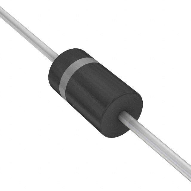
| 描述 | TVS DIODE 51VWM 82.4VC SOD123FTVS 二极管 - 瞬态电压抑制器 51V 200W 2.4A 5% Unidirectional |
| 产品分类 | |
| 品牌 | Littelfuse |
| 产品手册 | |
| 产品图片 |
|
| rohs | 符合RoHS含铅 / 符合限制有害物质指令(RoHS)规范要求 |
| 产品系列 | 二极管与整流器,TVS二极管,TVS 二极管 - 瞬态电压抑制器,Littelfuse SMF51ASMF |
| 数据手册 | |
| 产品型号 | SMF51A |
| 不同频率时的电容 | - |
| 产品培训模块 | http://www.digikey.cn/PTM/IndividualPTM.page?site=cn&lang=zhs&ptm=22970http://www.digikey.cn/PTM/IndividualPTM.page?site=cn&lang=zhs&ptm=25590 |
| 产品种类 | TVS 二极管 - 瞬态电压抑制器 |
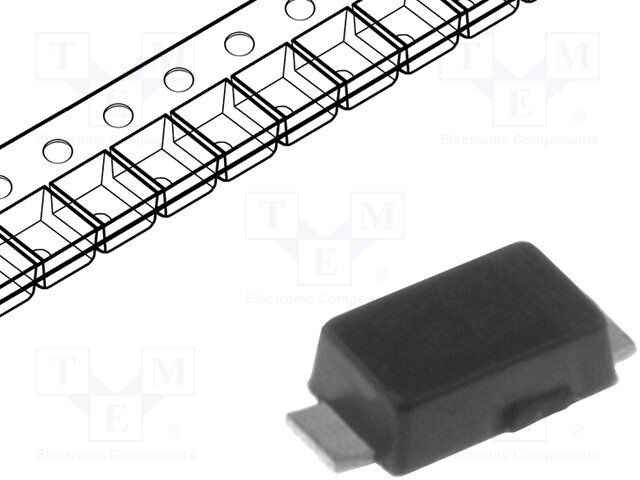
| 供应商器件封装 | SOD-123F |
| 其它名称 | F5833DKR |
| 击穿电压 | 56.7 V to 62.7 V |
| 功率-峰值脉冲 | 200W |
| 包装 | Digi-Reel® |
| 单向通道 | 1 |
| 双向通道 | - |
| 商标 | Littelfuse |
| 安装类型 | 表面贴装 |
| 安装风格 | SMD/SMT |
| 封装 | Reel |
| 封装/外壳 | SOD-123F |
| 封装/箱体 | SOD-123 |
| 峰值浪涌电流 | 2.4 A |
| 峰值脉冲功率耗散 | 200 W |
| 工作温度 | -55°C ~ 150°C (TJ) |
| 工厂包装数量 | 3000 |
| 应用 | 通用 |
| 最大工作温度 | + 150 C |
| 最小工作温度 | - 55 C |
| 极性 | Unidirectional |
| 标准包装 | 1 |
| 电压-击穿(最小值) | 56.7V |
| 电压-反向关态(典型值) | 51V |
| 电压-箝位(最大值)@Ipp | 82.4V |
| 电流-峰值脉冲(10/1000µs) | 2.4A |
| 电源线路保护 | 无 |
| 端接类型 | SMD/SMT |
| 类型 | 齐纳 |
| 系列 | SMF |
| 钳位电压 | 82.4 V |


- 商务部:美国ITC正式对集成电路等产品启动337调查
- 曝三星4nm工艺存在良率问题 高通将骁龙8 Gen1或转产台积电
- 太阳诱电将投资9.5亿元在常州建新厂生产MLCC 预计2023年完工
- 英特尔发布欧洲新工厂建设计划 深化IDM 2.0 战略
- 台积电先进制程称霸业界 有大客户加持明年业绩稳了
- 达到5530亿美元!SIA预计今年全球半导体销售额将创下新高
- 英特尔拟将自动驾驶子公司Mobileye上市 估值或超500亿美元
- 三星加码芯片和SET,合并消费电子和移动部门,撤换高东真等 CEO
- 三星电子宣布重大人事变动 还合并消费电子和移动部门
- 海关总署:前11个月进口集成电路产品价值2.52万亿元 增长14.8%


PDF Datasheet 数据手册内容提取
Transient Voltage Suppression Diodes Surface Mount – 200W > SMF Series SMF Series RoHS Pb e3 Description Uni-directional The SMF series is designed specifically to protect sensitive electronic equipment from voltage transients induced by lightning and other transient voltage events. SMF package is 50% smaller in footprint when compare to SMA package and deliverying one of the low height profiles (1.1mm) in the industry. Features • 200W peak pulsepower • ESD protection of data Agency Approvals capability at 10/1000µs lines in accordance with waveform, repetition rate IEC 61000-4-2 AGENCY AGENCY FILE NUMBER (duty cycle): 0.01% • EFT protection of data •Compatible with lines in accordance with E230531 industrial standard IEC 61000-4-4 package SOD-123FL • Fast response time: Maximum Ratings and Thermal Characteristics typically less than 1.0ns (T =25OC unless otherwise noted) • Low profile: maximum A height of 1.1mm. from 0 Volts to VBR min • Glass passivated junction • Low inductance, excellent Parameter Symbol Value Unit clamping capability • Built-in strain relief • For surface mounted • Plastic package is Peak Pulse Power Dissipation at P 200 W applications to optimize flammability rated T=25ºC by 10/1000µs (Note 1) PPM A board space V-0 per Underwriters Laboratories Thermal Resistance Junction- to- • High temperature R 220 °C/W Ambient θJA to reflow soldering • Meet MSL level1, per Thermal Resistance Junction- to- guaranteed: 260°C/40sec J-STD-020, LF maximun R 100 °C/W Lead θJL • Typical failure mode is peak of 260°C short from over-specified • Matte tin lead–free plated Operating Temperature Range T -65 to 150 °C J voltage or current • Halogen-free and RoHS • Whisker test is conducted compliant Storage Temperature Range T -65 to 175 °C STG based on JEDEC • Pb-free E3 means 2nd JESD201A per its table 4a level interconnect is Notes: 1. Non-repetitive current pulse, per Fig. 4 and derated above T (initial) =25ºC per Fig. 3. and 4c Pb-free and the terminal J • IEC-61000-4-2 ESD finish material is tin(Sn) 30kV(Air), 30kV (Contact) (IPC/ JEDEC J-STD- 609A.01) Functional Diagram Applications Bi-directional SMF devices are ideal for the protection of I/O interfaces, V bus and other vulnerable circuit used in cellular Cathode Anode CC phones, portable devices, business machines, power Uni-directional supplies and other consumer applications. Additional Infomarion Datasheet Resources Samples © 2017 Littelfuse, Inc. Specifications are subject to change without notice. Revised: 12/06/17
Transient Voltage Suppression Diodes Surface Mount – 200W > SMF Series Electrical Characteristics (T=25°C unless otherwise noted) A Breakdown Part Marking Voltage VBR Test Reverse Stand Maximum Maximum Maximum Agency (Volts) @ I Current Reverse Peak Pulse Clamping Approval Number Code T off Voltage I Leakage @ V Current I Voltage @I T VR (V) I (µA) R (A) pp V (V) pp MIN MAX (mA) R C SMF5.0A AE 6.40 7.00 10 5.0 400 21.7 9.2 X SMF6.0A AG 6.67 7.37 10 6.0 400 19.4 10.3 X SMF6.5A AK 7.22 7.98 10 6.5 250 17.9 11.2 X SMF7.0A AM 7.78 8.60 10 7.0 100 16.7 12.0 X SMF7.5A AP 8.33 9.21 1 7.5 50 15.5 12.9 X SMF8.0A AR 8.89 9.83 1 8.0 25 14.7 13.6 X SMF8.5A AT 9.44 10.40 1 8.5 10 13.9 14.4 X SMF9.0A AV 10.00 11.10 1 9.0 5 13.0 15.4 X SMF10A AX 11.10 12.30 1 10 2.5 11.8 17.0 X SMF11A AZ 12.20 13.50 1 11 2.5 11.0 18.2 X SMF12A BE 13.30 14.70 1 12 2.5 10.1 19.9 X SMF13A BG 14.40 15.90 1 13 1.0 9.3 21.5 X SMF14A BK 15.60 17.20 1 14 1.0 8.6 23.2 X SMF15A BM 16.70 18.50 1 15 1.0 8.2 24.4 X SMF16A BP 17.80 19.70 1 16 1.0 7.7 26.0 X SMF17A BR 18.90 20.90 1 17 1.0 7.2 27.6 X SMF18A BT 20.0 0 22.10 1 18 1.0 6.8 29.2 X SMF20A BV 22.20 24.50 1 20 1.0 6.2 32.4 X SMF22A BX 24.40 26.90 1 22 1.0 5.6 35.5 X SMF24A BZ 26.70 29.50 1 24 1.0 5.1 38.9 X SMF26A CE 28.90 31.90 1 26 1.0 4.8 42.1 X SMF28A CG 31.10 34.40 1 28 1.0 4.4 45.4 X SMF30A CK 33.30 36.80 1 30 1.0 4.1 48.4 X SMF33A CM 36.70 40.60 1 33 1.0 3.8 53.3 X SMF36A CP 40.00 44.20 1 36 1.0 3.4 58.1 X SMF40A CR 44.40 49.10 1 40 1.0 3.1 64.5 X SMF43A CT 47.80 52.80 1 43 1.0 2.9 69.4 X SMF45A CV 50.00 55.30 1 45 1.0 2.8 72.7 X SMF48A CX 53.30 58.90 1 48 1.0 2.6 77.4 X SMF51A CZ 56.70 62.70 1 51 1.0 2.4 82.4 X SMF54A DE 60.00 66.30 1 54 1.0 2.3 87.1 X SMF58A RG 64.40 71.20 1 58 1.0 2.1 93.6 SMF60A RK 66.70 73.70 1 60 1.0 1.8 96.8 SMF64A RM 71.10 78.60 1 64 1.0 1.7 103.0 SMF70A RP 77.80 86.00 1 70 1.0 1.5 113.0 SMF75A RR 83.30 92.10 1 75 1.0 1.4 121.0 SMF78A RT 86.70 95.80 1 78 1.0 1.4 126.0 SMF85A RV 94.40 104.00 1 85 1.0 1.3 137.0 SMF90A RW 100.00 111.00 1 90 1.0 1.2 146.0 SMF100A RX 111.00 123.00 1 100 1.0 1.1 162.0 Notes: 1. V measured after I applied for 300µs, I = square wave pulse or equivalent. BR T T 2. Surge current waveform per 10/1000µs exponential wave and derated per Fig.2. 3. All terms and symbols are consistent with ANSI/IEEE C62.35. © 2017 Littelfuse, Inc. Specifications are subject to change without notice. Revised: 12/06/17
Transient Voltage Suppression Diodes Surface Mount – 200W > SMF Series I-V Curve Characteristics Uni-directional Vc VBRVR V IRVF IT Ipp P Peak Pulse Power Dissipation -- Max power dissipation PPM V Stand-off Voltage -- Maximum voltage that can be applied to the TVS without operation R V Breakdown Voltage -- Maximum voltage that flows though the TVS at a specified test current (I) BR T V Clamping Voltage -- Peak voltage measured across the TVS at a specified Ippm (peak impulse current) C I Reverse Leakage Current -- Current measured at V R R V Forward Voltage Drop for Uni-directional F Ratings and Characteristic Curves (T=25°C unless otherwise noted) A Figure 1 - TVS Transients Clamping Waveform Figure 2 - Peak Pulse Power Rating Curve Voltage Transients 10 W) k Voltage Across TVS wer ( nt Po Curre Current Through TVS ulse 1 e or ak P Voltag P-PePPM 0.1 0.000001 0.00001 0.0001 0.001 t-Pulse Width (sec.) d Time continues on next page. © 2017 Littelfuse, Inc. Specifications are subject to change without notice. Revised: 12/06/17
Transient Voltage Suppression Diodes Surface Mount – 200W > SMF Series Ratings and Characteristic Curves (T=25°C unless otherwise noted) (Continued) A Figure 3 - Peak Pulse Power Derating Curve Figure 4 - Pulse Waveform - 10/1000µS 100 150 e Power (P) or Current (I)PPPPating in Percentage % 468000 eak Pulse Current, % IRSM 15000 tr=1PI0PeµPasMke cVaHIlPuaPelMf Va(lI Pu P12eTPac0M usuJ/ r1=)ltrsh02eee50n W °0tpC dµiodeistncehtac( wyt.ds hW) teiosar ev5d 0eteh%ffieon orpemfde IaPkP M ak PulsDer 20 I- PPPM as defined by R.E.A e P td 0 0 0 25 50 75 100 125 150 175 0 1.0 2.0 3.0 4.0 TJ - Initial Junction Temperature (ºC) t-Time (ms) Figure 5 - Forward Voltage Figure 6 - Typical Junction Capacitance 10000 0.9 e g olta 0.8 v d pe 0.7 p o 1000 dr d 0.6 ar Measured@Vr=0v w or cal f 0.5 pf) pi ( Ty 0.4 C j Measured@50%Vr V - f 100 0 -55 10 75 140 Temperature (ºC) Figure 7 - Peak Forward Voltage Drop vs. Figure 8 - Maximum Non-Repetitive Forward Surge 10 Peak Forward Current Current Uni-Directional Only 1 10 100 V - Reverse breakdown voltage br 35 A) A) 10 nt(30 Current( ve Curre25 ward 1 d Sur20 For war15 k or a F Pe 0.1 ak 10 -F Pe I M - 5 S F I 0.01 0 0 0.5 1 1.5 2 2.5 3 3.5 4 1 10 100 VF-Peak Forward Voltage(V) Number of Cycles at 60 Hz © 2017 Littelfuse, Inc. Specifications are subject to change without notice. Revised: 12/06/17
Transient Voltage Suppression Diodes Surface Mount – 200W > SMF Series Soldering Parameters Lead–free Reflow Condition assembly - Temperature Min (T ) 150°C TP tp s(min) Pre Heat -- TTeimmep e(mraitnu rteo Mmaaxx) ((Ttss()max)) 6200 0–° C180 secs (T)e Ts(mTaLx) Ramp-up tL CrTitiLc atol ZToPne Average ramp up rate (Liquidus Temp (T ) ur tTo pea tko T - Ramp-up Rate A 33°°CC//sseeccoonndd mmaaxx TemperatTs(min) Prethseat Ramp-down S(max) A - Temperature (T ) (Liquidus) 217°C Reflow A 25˚C - Time (min to max) (t) 60 – 150 seconds t 25˚C to Peak s Time (t) Peak Temperature (T) 260+0/-5 °C P Time within 5°C of actual peak 20 – 40 seconds Temperature (t) p Ramp-down Rate 6°C/second max Environmental Specifications Time 25°C to peak Temperature (T) 8 minutes Max. P Do not exceed 260°C High Temp. Storage JESD22-A103 HTRB JESD22-A108 Physical Specifications Temperature Cycling JESD22-A104 SOD-123FL plastic over glass passivated Case junction MSL JEDEC-J-STD-020, Level 1 Color band denotes cathode except Polarity bipolar H3TRB JESD22-A101 Matte tin-plated leads, solderable per Terminal JESD22-B102 RSH JESD22-A111 Dimensions - SOD-123FL Package Millimeters Inches Dimensions E Min Max Min Max A 2.50 2.90 0.0984 0.1142 A B B 3.40 3.90 0.1339 0.1535 C 0.70 1.20 0.0275 0.0472 D 1.50 2.00 0.0591 0.0787 E F E 0.35 0.90 0.0138 0.0354 C D F 0.05 0.26 0.0020 0.0102 G 0.00 0.10 0.000 0.0039 GH H 0.95 1.10 0.0374 0.0433 Mounting Pad Layout 1.6 (0.062) 1.3 (0.051) 1.4 (0.055) © 2017 Littelfuse, Inc. Specifications are subject to change without notice. Revised: 12/06/17
Transient Voltage Suppression Diodes Surface Mount – 200W > SMF Series Part Numbering System Part Marking System SMF xx A LF Cathode Band (for uni-directional products only) XX 5% VBR VOLTAGE TOLERANCE YM Marking Code Trace Code Marking Y:Year Code V VOLTAGE M: Month Code R SERIES Packaging Options Component Packaging Part number Quantity Packaging Option Package Specification SMFXXX SOD-123FL 3000 Tape & Reel – 8mm tape/7” reel EIA RS-481 SMFXXX-T13 SOD-123FL 10000 Tape & Reel – 8mm tape/13” reel EIA RS-481 Tape and Reel Specification 0.157 (4.0) Cathode 0.31 (8.0) 0.157 0.059 DIA Cover tape (4.0) (1.5) 7.0 (178) Dimensions are in inches 0.80 (20.2) (and millimeters). Arbor Hole Dia. Direction of Feed 0.33 (8.5) Disclaimer Notice - Information furnished is believed to be accurate and reliable. However, users should independently evaluate the suitability of and test each product selected for their own applications. Littelfuse products are not designed for, and may not be used in, all applications. Read complete Disclaimer Notice at www.littelfuse.com/disclaimer-electronics. © 2017 Littelfuse, Inc. Specifications are subject to change without notice. Revised: 12/06/17