ICGOO在线商城 > 分立半导体产品 > 晶体管 - FET,MOSFET - 单 > SI7617DN-T1-GE3
 Datasheet下载
- 型号: SI7617DN-T1-GE3
- 制造商: Vishay
- 库位|库存: xxxx|xxxx
- 要求:
| 数量阶梯 | 香港交货 | 国内含税 |
| +xxxx | $xxxx | ¥xxxx |
查看当月历史价格
查看今年历史价格
SI7617DN-T1-GE3产品简介:
ICGOO电子元器件商城为您提供SI7617DN-T1-GE3由Vishay设计生产,在icgoo商城现货销售,并且可以通过原厂、代理商等渠道进行代购。 SI7617DN-T1-GE3价格参考¥询价-¥询价。VishaySI7617DN-T1-GE3封装/规格:晶体管 - FET,MOSFET - 单, 表面贴装 P 沟道 30V 35A(Tc) 3.7W(Ta),52W(Tc) PowerPAK® 1212-8。您可以下载SI7617DN-T1-GE3参考资料、Datasheet数据手册功能说明书,资料中有SI7617DN-T1-GE3 详细功能的应用电路图电压和使用方法及教程。
Vishay Siliconix的SI7617DN-T1-GE3是一款N沟道增强型MOSFET(金属氧化物场效应晶体管),具有低导通电阻和快速开关特性,适用于多种电力电子应用。以下是该型号的主要应用场景:

 1. 电源管理
   SI7617DN-T1-GE3广泛应用于各种电源管理系统中,包括DC-DC转换器、降压/升压转换器、线性稳压器等。其低导通电阻(Rds(on))有助于减少功率损耗,提高效率,尤其适合需要高效能、低功耗的应用场景。

 2. 电机驱动
   在小型电机驱动电路中,如步进电机、直流无刷电机(BLDC)、伺服电机等,SI7617DN-T1-GE3可以作为开关元件,控制电机的启动、停止和调速。其快速开关特性和低导通电阻能够有效降低发热,延长设备寿命。

 3. 电池管理系统(BMS)
   在电池管理系统中,MOSFET用于电池充放电控制、过流保护和短路保护。SI7617DN-T1-GE3的低导通电阻和高可靠性使其成为理想的开关选择,确保电池在安全范围内工作,同时提高系统的整体效率。

 4. 消费电子产品
   该型号MOSFET常用于智能手机、平板电脑、笔记本电脑等消费电子产品的电源管理模块中。它能够提供高效的电源切换,支持快速充电功能,并且占用空间小,适合便携式设备的设计需求。

 5. 工业自动化
   在工业自动化领域,如PLC(可编程逻辑控制器)、传感器接口、继电器替代等应用中,SI7617DN-T1-GE3可以用作信号隔离和功率传输的开关元件。其耐用性和稳定性能够在恶劣的工业环境中保持可靠运行。

 6. 汽车电子
   在汽车电子系统中,如电动助力转向(EPS)、车身控制系统、LED照明驱动等,SI7617DN-T1-GE3能够承受较大的电流波动和温度变化,确保系统的稳定性和安全性。

总之,SI7617DN-T1-GE3凭借其出色的性能参数和可靠性,适用于广泛的电力电子应用场景,特别是在对效率和可靠性要求较高的场合。
| 参数 | 数值 |
| 产品目录 | |
| ChannelMode | Enhancement |
| 描述 | MOSFET P-CH 30V 35A 1212-8 PPAKMOSFET 30V 35A 52W 12.3mohm @ 10V |
| 产品分类 | FET - 单分离式半导体 |
| FET功能 | 标准 |
| FET类型 | MOSFET P 通道,金属氧化物 |
| Id-ContinuousDrainCurrent | - 35 A |
| Id-连续漏极电流 | - 35 A |
| 品牌 | Vishay / SiliconixVishay Siliconix |
| 产品手册 | |
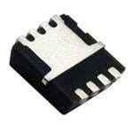
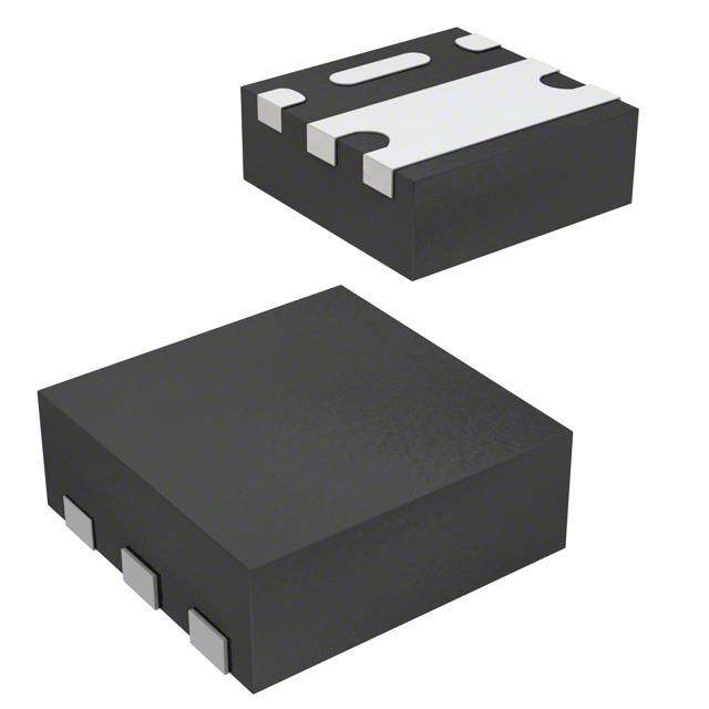
| 产品图片 |
|
| rohs | RoHS 合规性豁免无铅 / 符合限制有害物质指令(RoHS)规范要求 |
| 产品系列 | 晶体管,MOSFET,Vishay / Siliconix SI7617DN-T1-GE3TrenchFET® |
| 数据手册 | |
| 产品型号 | SI7617DN-T1-GE3SI7617DN-T1-GE3 |
| Pd-PowerDissipation | 52 W |
| Pd-功率耗散 | 52 W |
| Qg-GateCharge | 20.5 nC |
| Qg-栅极电荷 | 20.5 nC |
| RdsOn-Drain-SourceResistance | 12.3 mOhms |
| RdsOn-漏源导通电阻 | 12.3 mOhms |
| Vds-Drain-SourceBreakdownVoltage | - 30 V |
| Vds-漏源极击穿电压 | - 30 V |
| Vgs-Gate-SourceBreakdownVoltage | +/- 25 V |
| Vgs-栅源极击穿电压 | 25 V |
| 上升时间 | 43 ns |
| 下降时间 | 11 ns |
| 不同Id时的Vgs(th)(最大值) | 2.5V @ 250µA |
| 不同Vds时的输入电容(Ciss) | 1800pF @ 15V |
| 不同Vgs时的栅极电荷(Qg) | 59nC @ 10V |
| 不同 Id、Vgs时的 RdsOn(最大值) | 12.3 毫欧 @ 13.9A,10V |
| 产品种类 | MOSFET |
| 供应商器件封装 | PowerPAK® 1212-8 |
| 其它名称 | SI7617DN-T1-GE3CT |
| 典型关闭延迟时间 | 30 ns |
| 功率-最大值 | 52W |
| 包装 | 剪切带 (CT) |
| 商标 | Vishay / Siliconix |
| 安装类型 | 表面贴装 |
| 安装风格 | SMD/SMT |
| 封装 | Reel |
| 封装/外壳 | PowerPAK® 1212-8 |
| 封装/箱体 | PowerPAK 1212-8 |
| 工厂包装数量 | 3000 |
| 晶体管极性 | P-Channel |
| 最大工作温度 | + 150 C |
| 最小工作温度 | - 55 C |
| 标准包装 | 1 |
| 正向跨导-最小值 | 35 S |
| 漏源极电压(Vdss) | 30V |
| 电流-连续漏极(Id)(25°C时) | 35A (Tc) |
| 通道模式 | Enhancement |
| 配置 | Single |
| 零件号别名 | SI7617DN-GE3 |


PDF Datasheet 数据手册内容提取
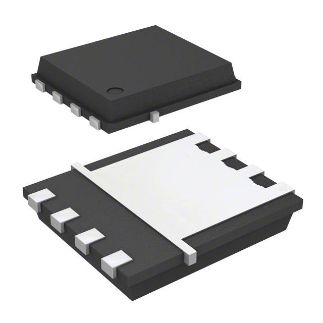
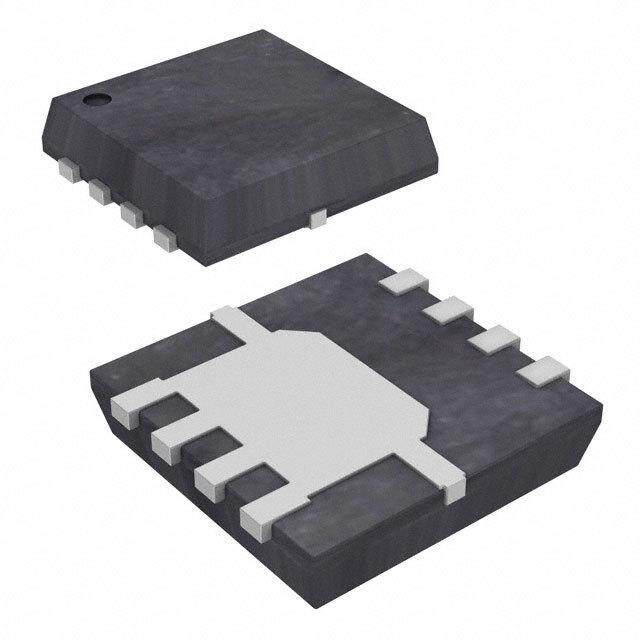
Si7617DN www.vishay.com Vishay Siliconix P-Channel 30-V (D-S) MOSFET FEATURES PRODUCT SUMMARY • TrenchFET® power MOSFET V (V) R (Ω) I (A) d, g Q (TYP.) DS DS(on) D g • 100 % R and UIS tested 0.0123 at V = -10 V -35 g GS -30 20.5 nC • Material categorization: 0.0222 at V = -4.5 V -35 GS for definitions of compliance please see PowerPAK® 1212-8 Single www.vishay.com/doc?99912 D D D7 8 APPLICATIONS S D 6 5 • Notebook battery charging • Notebook adapter switch G 3.3 2 SS11 mm 1 3.3 m m 4 S3 S G Top View Bottom View D Ordering Information: P-Channel MOSFET Si7617DN-T1-GE3 (Lead (Pb)-free and halogen-free) ABSOLUTE MAXIMUM RATINGS (T = 25 °C, unless otherwise noted) A PARAMETER SYMBOL LIMIT UNIT Drain-Source Voltage V -30 DS V Gate-Source Voltage V ± 25 GS T = 25 °C -35 d C T = 70 °C -35 d C Continuous Drain Current (T = 150 °C) I J T = 25 °C D -13.9 a, b A T = 70 °C -11.1 a, b A A Pulsed Drain Current I -60 DM T = 25 °C -35 d C Continuous Source-Drain Diode Current I T = 25 °C S -3 a, b A Avalanche Current I -29 AS L = 0.1 mH Single-Pulse Avalanche Energy E 42 mJ AS T = 25 °C 52 C T = 70 °C 33 C Maximum Power Dissipation P W T = 25 °C D 3.7 a, b A T = 70 °C 2.4 a, b A Operating Junction and Storage Temperature Range T , T -55 to +150 J stg °C Soldering Recommendations (Peak Temperature) e, f 260 THERMAL RESISTANCE RATINGS PARAMETER SYMBOL TYPICAL MAXIMUM UNIT Maximum Junction-to-Ambient a, c t ≤ 10 s R 26 33 thJA °C/W Maximum Junction-to-Case Steady State R 1.9 2.4 thJC Notes a. Surface mounted on 1" x 1" FR4 board. b. t = 10 s. c. Maximum under steady state conditions is 81 °C/W. d. Package limited. e. See solder profile (www.vishay.com/doc?73257). The PowerPAK 1212-8 is a leadless package. The end of the lead terminal is exposed copper (not plated) as a result of the singulation process in manufacturing. A solder fillet at the exposed copper tip cannot be guaranteed and is not required to ensure adequate bottom side solder interconnection. f. Rework conditions: manual soldering with a soldering iron is not recommended for leadless components. g. Based on T = 25 °C. C S15-1032-Rev. B, 04-May-15 1 Document Number: 65164 For technical questions, contact: pmostechsupport@vishay.com THIS DOCUMENT IS SUBJECT TO CHANGE WITHOUT NOTICE. THE PRODUCTS DESCRIBED HEREIN AND THIS DOCUMENT ARE SUBJECT TO SPECIFIC DISCLAIMERS, SET FORTH AT www.vishay.com/doc?91000
Si7617DN www.vishay.com Vishay Siliconix SPECIFICATIONS (T = 25 °C, unless otherwise noted) J PARAMETER SYMBOL TEST CONDITIONS MIN. TYP. MAX. UNIT Static Drain-Source Breakdown Voltage V V = 0 V, I = -250 μA -30 - - V DS GS D V Temperature Coefficient ΔV /T - -25 - DS DS J I = -250 μA mV/°C V Temperature Coefficient ΔV /T D - 4.7 - GS(th) GS(th) J Gate-Source Threshold Voltage V V = V , I = -250 μA -1.2 - -2.5 V GS(th) DS GS D Gate-Source Leakage I V = 0 V, V = ± 25 V - - ± 100 nA GSS DS GS V = -30 V, V = 0 V - - -1 DS GS Zero Gate Voltage Drain Current I μA DSS V = -30 V, V = 0 V, T = 55 °C - - -5 DS GS J On-State Drain Current a I V ≥ -10 V, V = -10 V -30 - - A D(on) DS GS V = -10 V, I = -13.9 A - 0.0103 0.0123 Drain-Source On-State Resistance a R GS D Ω DS(on) V = -4.5 V, I = -10.3 A - 0.0185 0.0222 GS D Forward Transconductance a g V = -15 V, I = -13.9 A - 35 - S fs DS D Dynamic b Input Capacitance C - 1800 - iss Output Capacitance C V = -15 V, V = 0 V, f = 1 MHz - 370 - pF oss DS GS Reverse Transfer Capacitance C - 312 - rss V = -15 V, V = -10 V, I = -13.9 A - 39 59 DS GS D Total Gate Charge Q g - 20.5 31 nC Gate-Source Charge Q V = -15 V, V = -4.5 V, I = -13.9 A - 6 - gs DS GS D Gate-Drain Charge Q - 11 - gd Gate Resistance R f = 1 MHz 0.4 2 4 Ω g Turn-On Delay Time t - 11 22 d(on) Rise Time tr VDD = -15 V, RL = 1.35 Ω - 9 18 Turn-Off DelayTime td(off) ID ≅ -11.1 A, VGEN = -10 V, Rg = 1 Ω - 32 50 Fall Time t - 9 18 f ns Turn-On Delay Time t - 40 60 d(on) Rise Time tr VDD = -15 V, RL = 1.35 Ω - 43 65 Turn-Off DelayTime td(off) ID ≅ -11.1 A, VGEN = -4.5 V, Rg = 1 Ω - 30 45 Fall Time t - 11 22 f Drain-Source Body Diode Characteristics Continuous Source-Drain Diode I T = 25 °C - - -35 Current S C A Pulse Diode Forward Current I - - -60 SM Body Diode Voltage V I = -11.1 A, V = 0 V - -0.8 -1.2 V SD S GS Body Diode Reverse Recovery Time t - 33 50 ns rr Body Diode Reverse Recovery Charge Qrr IF = -11.1 A, dI/dt = 100 A/μs, - 30 45 nC Reverse Recovery Fall Time ta TJ = 25 °C - 18 - ns Reverse Recovery Rise Time t - 16 - b Notes a. Pulse test; pulse width ≤ 300 μs, duty cycle ≤ 2 %. b. Guaranteed by design, not subject to production testing. Stresses beyond those listed under “Absolute Maximum Ratings” may cause permanent damage to the device. These are stress ratings only, and functional operation of the device at these or any other conditions beyond those indicated in the operational sections of the specifications is not implied. Exposure to absolute maximum rating conditions for extended periods may affect device reliability. S15-1032-Rev. B, 04-May-15 2 Document Number: 65164 For technical questions, contact: pmostechsupport@vishay.com THIS DOCUMENT IS SUBJECT TO CHANGE WITHOUT NOTICE. THE PRODUCTS DESCRIBED HEREIN AND THIS DOCUMENT ARE SUBJECT TO SPECIFIC DISCLAIMERS, SET FORTH AT www.vishay.com/doc?91000
Si7617DN www.vishay.com Vishay Siliconix TYPICAL CHARACTERISTICS (25 °C, unless otherwise noted) 60 1.0 VGS=10Vthru5V 0.8 45 A) A) ent ( VGS=4V ent ( 0.6 Curr 30 Curr TC=125 °C n n Drai Drai 0.4 - D - D TC=25 °C I 15 I 0.2 VGS=3V TC=- 55 °C 0 0.0 0 1 2 3 4 0 1 2 3 4 VDS- Drain-to-SourceVoltage(V) VGS- Gate-to-Source Voltage (V) Output Characteristics Transfer Characteristics 0.030 3000 Ciss 0.024 2400 Ωe () VGS=4.5V F) c p an 0.018 e ( 1800 sist anc Re cit n- pa O 0.012 a 1200 - S(on) VGS=10V C - C Coss D R 0.006 600 Crss 0.000 0 0 15 30 45 60 0 5 10 15 20 25 30 ID - Drain Current (A) VDS- Drain-to-SourceVoltage(V) On-Resistance vs. Drain Current Capacitance 10 1.8 ID=13.9A d) ID=13.9A e e(V) 8 maliz 1.5 VGS=4.5V oltag VDS=8V (Nor VGS=10V V 6 e Source VDS=15V sistanc 1.2 e-to- 4 n-Re - GatGS 2 VDS=24V - OS(on) 0.9 V D R 0 0.6 0 10 20 30 40 - 50 - 25 0 25 50 75 100 125 150 Qg- TotalGateCharge(nC) TJ- JunctionTemperature(°C) Gate Charge On-Resistance vs. Junction Temperature S15-1032-Rev. B, 04-May-15 3 Document Number: 65164 For technical questions, contact: pmostechsupport@vishay.com THIS DOCUMENT IS SUBJECT TO CHANGE WITHOUT NOTICE. THE PRODUCTS DESCRIBED HEREIN AND THIS DOCUMENT ARE SUBJECT TO SPECIFIC DISCLAIMERS, SET FORTH AT www.vishay.com/doc?91000
Si7617DN www.vishay.com Vishay Siliconix TYPICAL CHARACTERISTICS (25 °C, unless otherwise noted) 100 0.04 nt(A) 10 Ωance () 0.03 urceCurre On-Resist 0.02 TJ=125 °C - SoIS 1 TJ=150 °C TJ=25 °C - DS(on) 0.01 R TJ=25 °C 0.1 0 0.0 0.2 0.4 0.6 0.8 1.0 1.2 2 4 6 8 10 VSD- Source-to-DrainVoltage(V) VGS- Gate-to-SourceVoltage(V) Source-Drain Diode Forward Voltage On-Resistance vs. Gate-to-Source Voltage 2.2 50 ID=250µA 40 1.9 V) W) 30 V( GS(th) 1.6 Power ( 20 1.3 10 1.0 0 - 50 - 25 0 25 50 75 100 125 150 0.01 0.1 1 10 100 1000 TJ- Temperature(°C) Time (s) Threshold Voltage Single Pulse Power, Junction-to-Ambient 100 LimitedbyRDS(on)* 100µs 10 A) 1ms ent ( 10ms urr 1 C n 100ms ai Dr 1s - D 10s I 0.1 DC TA=25 °C BVDSS SinglePulse Limited 0.01 0.1 1 10 100 VDS- Drain-to-SourceVoltage(V) *VGS>minimumVGSatwhichRDS(on)isspecified Safe Operating Area S15-1032-Rev. B, 04-May-15 4 Document Number: 65164 For technical questions, contact: pmostechsupport@vishay.com THIS DOCUMENT IS SUBJECT TO CHANGE WITHOUT NOTICE. THE PRODUCTS DESCRIBED HEREIN AND THIS DOCUMENT ARE SUBJECT TO SPECIFIC DISCLAIMERS, SET FORTH AT www.vishay.com/doc?91000
Si7617DN www.vishay.com Vishay Siliconix TYPICAL CHARACTERISTICS (25 °C, unless otherwise noted) 60 45 A) nt ( PackageLimited e Curr 30 n ai Dr - D I 15 0 0 25 50 75 100 125 150 TC- CaseTemperature(°C) Current Derating* 75 2.0 60 1.5 W) 45 W) wer ( wer ( 1.0 Po 30 Po 0.5 15 0 0.0 0 25 50 75 100 125 150 0 25 50 75 100 125 150 TC- CaseTemperature(°C) TA- AmbientTemperature(°C) Power Derating, Junction-to-Case Power Derating, Junction-to-Ambient * The power dissipation P is based on T (max.) = 150 °C, using junction-to-case thermal resistance, and is more useful in settling the upper D J dissipation limit for cases where additional heatsinking is used. It is used to determine the current rating, when this rating falls below the package limit. S15-1032-Rev. B, 04-May-15 5 Document Number: 65164 For technical questions, contact: pmostechsupport@vishay.com THIS DOCUMENT IS SUBJECT TO CHANGE WITHOUT NOTICE. THE PRODUCTS DESCRIBED HEREIN AND THIS DOCUMENT ARE SUBJECT TO SPECIFIC DISCLAIMERS, SET FORTH AT www.vishay.com/doc?91000
Si7617DN www.vishay.com Vishay Siliconix TYPICAL CHARACTERISTICS (25 °C, unless otherwise noted) 1 DutyCycle=0.5 nt e Transiance 0.2 ctivemped 0.1 0.1 Notes: eI Effmal 0.05 PDM eder NormalizTh 0.02 1.DutyCyt1clet,2D= tt12 2.PerUnitBase=RthJA=81 °C/W SinglePulse 3.TJM-TA=PDMZthJA(t) 4.SurfaceMounted 0.01 10-4 10-3 10-2 10-1 1 10 100 1000 SquareWavePulseDuration(s) Normalized Thermal Transient Impedance, Junction-to-Ambient 1 DutyCycle=0.5 nt EffectiveTransiemalImpedance 0.1 00.1.2 0.05 eder 0.02 zh aliT m or SinglePulse N 0.01 10-4 10-3 10-2 10-1 1 SquareWavePulseDuration(s) Normalized Thermal Transient Impedance, Junction-to-Case Vishay Siliconix maintains worldwide manufacturing capability. Products may be manufactured at one of several qualified locations. Reliability data for Silicon Technology and Package Reliability represent a composite of all qualified locations. For related documents such as package/tape drawings, part marking, and reliability data, see www.vishay.com/ppg?65164. S15-1032-Rev. B, 04-May-15 6 Document Number: 65164 For technical questions, contact: pmostechsupport@vishay.com THIS DOCUMENT IS SUBJECT TO CHANGE WITHOUT NOTICE. THE PRODUCTS DESCRIBED HEREIN AND THIS DOCUMENT ARE SUBJECT TO SPECIFIC DISCLAIMERS, SET FORTH AT www.vishay.com/doc?91000
Package Information www.vishay.com Vishay Siliconix PowerPAK® 1212-8, (Single / Dual) L H E2 K W D4 E4 θ 8 M 1 1 e Z 2 2 D1 D D2 D5 3 4 5 4b θ L1 E3 θ θ A1 Backside view of single pad L A H E2 K E4 c H 4 2 D 1 E1 Detail Z 2x) D1 E D3( 2 2 5 D D Notes 3 1 1. Inch will govern K 2 Dimensions exclusive of mold gate burrs D2 4b 3. Dimensions exclusive of mold flash and cutting burrs E3 Backside view of dual pad MILLIMETERS INCHES DIM. MIN. NOM. MAX. MIN. NOM. MAX. A 0.97 1.04 1.12 0.038 0.041 0.044 A1 0.00 - 0.05 0.000 - 0.002 b 0.23 0.30 0.41 0.009 0.012 0.016 c 0.23 0.28 0.33 0.009 0.011 0.013 D 3.20 3.30 3.40 0.126 0.130 0.134 D1 2.95 3.05 3.15 0.116 0.120 0.124 D2 1.98 2.11 2.24 0.078 0.083 0.088 D3 0.48 - 0.89 0.019 - 0.035 D4 0.47 typ. 0.0185 typ D5 2.3 typ. 0.090 typ E 3.20 3.30 3.40 0.126 0.130 0.134 E1 2.95 3.05 3.15 0.116 0.120 0.124 E2 1.47 1.60 1.73 0.058 0.063 0.068 E3 1.75 1.85 1.98 0.069 0.073 0.078 E4 0.034 typ. 0.013 typ. e 0.65 BSC 0.026 BSC K 0.86 typ. 0.034 typ. K1 0.35 - - 0.014 - - H 0.30 0.41 0.51 0.012 0.016 0.020 L 0.30 0.43 0.56 0.012 0.017 0.022 L1 0.06 0.13 0.20 0.002 0.005 0.008 0° - 12° 0° - 12° W 0.15 0.25 0.36 0.006 0.010 0.014 M 0.125 typ. 0.005 typ. ECN: S16-2667-Rev. M, 09-Jan-17 DWG: 5882 Revison: 09-Jan-17 1 Document Number: 71656 For technical questions, contact: pmostechsupport@vishay.com THIS DOCUMENT IS SUBJECT TO CHANGE WITHOUT NOTICE. THE PRODUCTS DESCRIBED HEREIN AND THIS DOCUMENT ARE SUBJECT TO SPECIFIC DISCLAIMERS, SET FORTH AT www.vishay.com/doc?91000
AN822 Vishay Siliconix ® PowerPAK 1212 Mounting and Thermal Considerations Johnson Zhao MOSFETs for switching applications are now available The PowerPAK 1212-8 has a footprint area compara- with die on resistances around 1 mΩ and with the ble to TSOP-6. It is over 40 % smaller than standard capability to handle 85 A. While these die capabilities TSSOP-8. Its die capacity is more than twice the size represent a major advance over what was available of the standard TSOP-6’s. It has thermal performance just a few years ago, it is important for power MOSFET an order of magnitude better than the SO-8, and 20 packaging technology to keep pace. It should be obvi- times better than TSSOP-8. Its thermal performance is ous that degradation of a high performance die by the better than all current SMT packages in the market. It package is undesirable. PowerPAK is a new package will take the advantage of any PC board heat sink technology that addresses these issues. The PowerPAK capability. Bringing the junction temperature down also 1212-8 provides ultra-low thermal impedance in a increases the die efficiency by around 20 % compared small package that is ideal for space-constrained with TSSOP-8. For applications where bigger pack- applications. In this application note, the PowerPAK ages are typically required solely for thermal consider- 1212-8’s construction is described. Following this, ation, the PowerPAK 1212-8 is a good option. mounting information is presented. Finally, thermal Both the single and dual PowerPAK 1212-8 utilize the and electrical performance is discussed. same pin-outs as the single and dual PowerPAK SO-8. The low 1.05 mm PowerPAK height profile makes both THE PowerPAK PACKAGE versions an excellent choice for applications with The PowerPAK 1212-8 package (Figure 1) is a deriva- space constraints. tive of PowerPAK SO-8. It utilizes the same packaging technology, maximizing the die area. The bottom of the PowerPAK 1212 SINGLE MOUNTING die attach pad is exposed to provide a direct, low resis- To take the advantage of the single PowerPAK 1212-8’s tance thermal path to the substrate the device is thermal performance see Application Note 826, mounted on. The PowerPAK 1212-8 thus translates the benefits of the PowerPAK SO-8 into a smaller Recommended Minimum Pad Patterns With Outline package, with the same level of thermal performance. Drawing Access for Vishay Siliconix MOSFETs. Click on the PowerPAK 1212-8 single in the index of this (Please refer to application note “PowerPAK SO-8 document. Mounting and Thermal Considerations.”) In this figure, the drain land pattern is given to make full contact to the drain pad on the PowerPAK package. This land pattern can be extended to the left, right, and top of the drawn pattern. This extension will serve to increase the heat dissipation by decreasing the ther- mal resistance from the foot of the PowerPAK to the PC board and therefore to the ambient. Note that increasing the drain land area beyond a certain point will yield little decrease in foot-to-board and foot-to- ambient thermal resistance. Under specific conditions of board configuration, copper weight, and layer stack, experiments have found that adding copper beyond an area of about 0.3 to 0.5 in2 of will yield little improve- ment in thermal performance. Figure 1. PowerPAK 1212 Devices Document Number 71681 www.vishay.com 03-Mar-06 1
AN822 Vishay Siliconix PowerPAK 1212 DUAL To take the advantage of the dual PowerPAK 1212-8’s ture profile used, and the temperatures and time thermal performance, the minimum recommended duration, are shown in Figures 2 and 3. For the lead land pattern can be found in Application Note 826, (Pb)-free solder profile, see http://www.vishay.com/ Recommended Minimum Pad Patterns With Outline doc?73257. Drawing Access for Vishay Siliconix MOSFETs. Click on the PowerPAK 1212-8 dual in the index of this doc- ument. The gap between the two drain pads is 10 mils. This matches the spacing of the two drain pads on the Pow- erPAK 1212-8 dual package. This land pattern can be extended to the left, right, and top of the drawn pattern. This extension will serve to increase the heat dissipation by decreasing the ther- mal resistance from the foot of the PowerPAK to the PC board and therefore to the ambient. Note that increasing the drain land area beyond a certain point will yield little decrease in foot-to-board and foot-to- ambient thermal resistance. Under specific conditions of board configuration, copper weight, and layer stack, experiments have found that adding copper beyond an Ramp-Up Rate + 6 °C /Second Maximum area of about 0.3 to 0.5 in2 of will yield little improve- Temperature at 155 ± 15 °C 120 Seconds Maximum ment in thermal performance. Temperature Above 180 °C 70 - 180 Seconds Maximum Temperature 240 + 5/- 0 °C Time at Maximum Temperature 20 - 40 Seconds REFLOW SOLDERING Ramp-Down Rate + 6 °C/Second Maximum Vishay Siliconix surface-mount packages meet solder reflow reliability requirements. Devices are subjected Figure 2. Solder Reflow Temperature Profile to solder reflow as a preconditioning test and are then reliability-tested using temperature cycle, bias humid- ity, HAST, or pressure pot. The solder reflow tempera- 10 s (max) 210 - 220 °C 3 °C/s (max) 4 °C/s (max) 183 °C 140 - 170 °C 50 s (max) 3° C/s (max) 60 s (min) Reflow Zone Pre-Heating Zone Maximum peak temperature at 240 °C is allowed. Figure 3. Solder Reflow Temperatures and Time Durations www.vishay.com Document Number 71681 2 03-Mar-06
AN822 Vishay Siliconix TABLE 1: EQIVALENT STEADY STATE PERFORMANCE Package SO-8 TSSOP-8 TSOP-8 PPAK 1212 PPAK SO-8 Configuration Single Dual Single Dual Single Dual Single Dual Single Dual Thermal Resiatance R (C/W) 20 40 52 83 40 90 2.4 5.5 1.8 5.5 thJC PowerPAK 1212 Standard SO-8 Standard TSSOP-8 TSOP-6 49.8 °C 85 °C 149 °C 125 °C 2.4 °C/W 20 °C/W 52 °C/W 40 °C/W PC Board at 45 °C Figure 4. Temperature of Devices on a PC Board THERMAL PERFORMANCE Introduction Spreading Copper A basic measure of a device’s thermal performance is Designers add additional copper, spreading copper, to the junction-to-case thermal resistance, Rθjc, or the the drain pad to aid in conducting heat from a device. It junction to- foot thermal resistance, Rθjf. This parameter is helpful to have some information about the thermal is measured for the device mounted to an infinite heat performance for a given area of spreading copper. sink and is therefore a characterization of the device Figure 5 and Figure 6 show the thermal resistance of a only, in other words, independent of the properties of the PowerPAK 1212-8 single and dual devices mounted on object to which the device is mounted. Table 1 shows a a 2-in. x 2-in., four-layer FR-4 PC boards. The two inter- comparison of the PowerPAK 1212-8, PowerPAK SO-8, nal layers and the backside layer are solid copper. The standard TSSOP-8 and SO-8 equivalent steady state internal layers were chosen as solid copper to model the performance. large power and ground planes common in many appli- By minimizing the junction-to-foot thermal resistance, the cations. The top layer was cut back to a smaller area and MOSFET die temperature is very close to the tempera- at each step junction-to-ambient thermal resistance ture of the PC board. Consider four devices mounted on measurements were taken. The results indicate that an a PC board with a board temperature of 45 °C (Figure 4). area above 0.2 to 0.3 square inches of spreading copper Suppose each device is dissipating 2 W. Using the junc- gives no additional thermal performance improvement. tion-to-foot thermal resistance characteristics of the A subsequent experiment was run where the copper on PowerPAK 1212-8 and the other SMT packages, die the back-side was reduced, first to 50 % in stripes to temperatures are determined to be 49.8 °C for the Pow- mimic circuit traces, and then totally removed. No signif- erPAK 1212-8, 85 °C for the standard SO-8, 149 °C for icant effect was observed. standard TSSOP-8, and 125 °C for TSOP-6. This is a 4.8 °C rise above the board temperature for the Power- PAK 1212-8, and over 40 °C for other SMT packages. A 4.8 °C rise has minimal effect on r whereas a rise DS(ON) of over 40 °C will cause an increase in r as high DS(ON) as 20 %. Document Number 71681 www.vishay.com 03-Mar-06 3
AN822 Vishay Siliconix 105 130 Spreading Copper (sq. in.) 120 Spreading Copper (sq. in.) 95 110 85 100 W) W) C/ 75 C/ 90 R(°AJht 65 R(°AJ ht 80 50 % 100 % 70 100 % 55 0 % 50 % 60 0 % 45 50 0.00 0.25 0.50 0.75 1.00 1.25 1.50 1.75 2.00 0.00 0.25 0.50 0.75 1.00 1.25 1.50 1.75 2.00 Figure 5. Spreading Copper - Si7401DN Figure 6. Spreading Copper - Junction-to-Ambient Performance CONCLUSIONS As a derivative of the PowerPAK SO-8, the PowerPAK The PowerPAK 1212-8 combines small size with attrac- 1212-8 uses the same packaging technology and has tive thermal characteristics. By minimizing the thermal been shown to have the same level of thermal perfor- rise above the board temperature, PowerPAK simplifies mance while having a footprint that is more than 40 % thermal design considerations, allows the device to run smaller than the standard TSSOP-8. cooler, keeps r low, and permits the device to DS(ON) Recommended PowerPAK 1212-8 land patterns are handle more current than a same- or larger-size MOS- provided to aid in PC board layout for designs using this FET die in the standard TSSOP-8 or SO-8 packages. new package. www.vishay.com Document Number 71681 4 03-Mar-06
Application Note 826 Vishay Siliconix RECOMMENDED MINIMUM PADS FOR PowerPAK® 1212-8 Single 0.152 (3.860) 0.039 0.068 0.010 (0.990) (1.725) (0.255) 0.016 (0.405) 8 5) 4 0) 8 3 9 9 0 2 0 3 0. 2. 0. 2. ( ( 0.026 (0.660) 0.025 0.030 (0.635) (0.760) Recommended Minimum Pads Dimensions in Inches/(mm) Return to Index Return to Index A P P L I C A T I O N N O T E Document Number: 72597 www.vishay.com Revision: 21-Jan-08 7
Legal Disclaimer Notice www.vishay.com Vishay Disclaimer ALL PRODUCT, PRODUCT SPECIFICATIONS AND DATA ARE SUBJECT TO CHANGE WITHOUT NOTICE TO IMPROVE RELIABILITY, FUNCTION OR DESIGN OR OTHERWISE. Vishay Intertechnology, Inc., its affiliates, agents, and employees, and all persons acting on its or their behalf (collectively, “Vishay”), disclaim any and all liability for any errors, inaccuracies or incompleteness contained in any datasheet or in any other disclosure relating to any product. Vishay makes no warranty, representation or guarantee regarding the suitability of the products for any particular purpose or the continuing production of any product. To the maximum extent permitted by applicable law, Vishay disclaims (i) any and all liability arising out of the application or use of any product, (ii) any and all liability, including without limitation special, consequential or incidental damages, and (iii) any and all implied warranties, including warranties of fitness for particular purpose, non-infringement and merchantability. Statements regarding the suitability of products for certain types of applications are based on Vishay’s knowledge of typical requirements that are often placed on Vishay products in generic applications. Such statements are not binding statements about the suitability of products for a particular application. It is the customer’s responsibility to validate that a particular product with the properties described in the product specification is suitable for use in a particular application. Parameters provided in datasheets and / or specifications may vary in different applications and performance may vary over time. All operating parameters, including typical parameters, must be validated for each customer application by the customer’s technical experts. Product specifications do not expand or otherwise modify Vishay’s terms and conditions of purchase, including but not limited to the warranty expressed therein. Except as expressly indicated in writing, Vishay products are not designed for use in medical, life-saving, or life-sustaining applications or for any other application in which the failure of the Vishay product could result in personal injury or death. Customers using or selling Vishay products not expressly indicated for use in such applications do so at their own risk. Please contact authorized Vishay personnel to obtain written terms and conditions regarding products designed for such applications. No license, express or implied, by estoppel or otherwise, to any intellectual property rights is granted by this document or by any conduct of Vishay. Product names and markings noted herein may be trademarks of their respective owners. © 2017 VISHAY INTERTECHNOLOGY, INC. ALL RIGHTS RESERVED Revision: 08-Feb-17 1 Document Number: 91000
Mouser Electronics Authorized Distributor Click to View Pricing, Inventory, Delivery & Lifecycle Information: V ishay: SI7617DN-T1-GE3