ICGOO在线商城 > 分立半导体产品 > 晶体管 - FET,MOSFET - 单 > SI7106DN-T1-GE3
 Datasheet下载
- 型号: SI7106DN-T1-GE3
- 制造商: Vishay
- 库位|库存: xxxx|xxxx
- 要求:
| 数量阶梯 | 香港交货 | 国内含税 |
| +xxxx | $xxxx | ¥xxxx |
查看当月历史价格
查看今年历史价格
SI7106DN-T1-GE3产品简介:
ICGOO电子元器件商城为您提供SI7106DN-T1-GE3由Vishay设计生产,在icgoo商城现货销售,并且可以通过原厂、代理商等渠道进行代购。 SI7106DN-T1-GE3价格参考。VishaySI7106DN-T1-GE3封装/规格:晶体管 - FET,MOSFET - 单, 表面贴装 N 沟道 20V 12.5A(Ta) 1.5W(Ta) PowerPAK® 1212-8。您可以下载SI7106DN-T1-GE3参考资料、Datasheet数据手册功能说明书,资料中有SI7106DN-T1-GE3 详细功能的应用电路图电压和使用方法及教程。
| 参数 | 数值 |
| 产品目录 | |
| ChannelMode | Enhancement |
| 描述 | MOSFET N-CH 20V 12.5A 1212-8MOSFET 20V 19.5A 3.8W 6.2mohm @ 4.5V |
| 产品分类 | FET - 单分离式半导体 |
| FET功能 | 逻辑电平栅极,2.5V 驱动 |
| FET类型 | MOSFET N 通道,金属氧化物 |
| Id-ContinuousDrainCurrent | 12.5 A |
| Id-连续漏极电流 | 12.5 A |
| 品牌 | Vishay / SiliconixVishay Siliconix |
| 产品手册 | |
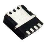
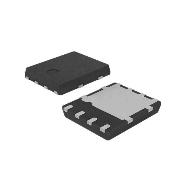
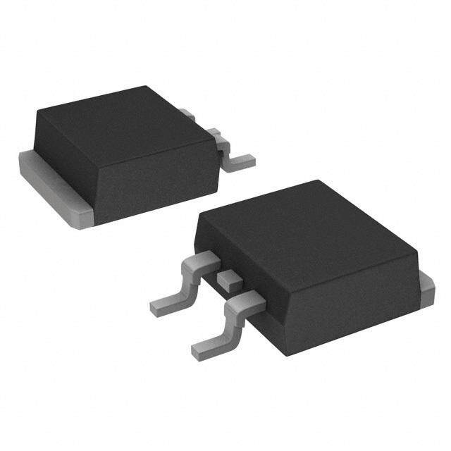
| 产品图片 |
|
| rohs | 符合RoHS无铅 / 符合限制有害物质指令(RoHS)规范要求 |
| 产品系列 | 晶体管,MOSFET,Vishay / Siliconix SI7106DN-T1-GE3TrenchFET® |
| 数据手册 | |
| 产品型号 | SI7106DN-T1-GE3SI7106DN-T1-GE3 |
| Pd-PowerDissipation | 1.5 W |
| Pd-功率耗散 | 1.5 W |
| RdsOn-Drain-SourceResistance | 6.2 mOhms |
| RdsOn-漏源导通电阻 | 6.2 mOhms |
| Vds-Drain-SourceBreakdownVoltage | 20 V |
| Vds-漏源极击穿电压 | 20 V |
| Vgs-Gate-SourceBreakdownVoltage | +/- 12 V |
| Vgs-栅源极击穿电压 | 12 V |
| 上升时间 | 15 ns |
| 下降时间 | 15 ns |
| 不同Id时的Vgs(th)(最大值) | 1.5V @ 250µA |
| 不同Vds时的输入电容(Ciss) | - |
| 不同Vgs时的栅极电荷(Qg) | 27nC @ 4.5V |
| 不同 Id、Vgs时的 RdsOn(最大值) | 6.2 毫欧 @ 19.5A,4.5V |
| 产品目录页面 | |
| 产品种类 | MOSFET |
| 供应商器件封装 | PowerPAK® 1212-8 |
| 其它名称 | SI7106DN-T1-GE3TR |
| 典型关闭延迟时间 | 50 ns |
| 功率-最大值 | 1.5W |
| 包装 | 带卷 (TR) |
| 商标 | Vishay / Siliconix |
| 商标名 | TrenchFET/PowerPAK |
| 安装类型 | 表面贴装 |
| 安装风格 | SMD/SMT |
| 封装 | Reel |
| 封装/外壳 | PowerPAK® 1212-8 |
| 封装/箱体 | PowerPAK 1212-8 |
| 工厂包装数量 | 3000 |
| 晶体管极性 | N-Channel |
| 最大工作温度 | + 150 C |
| 最小工作温度 | - 55 C |
| 标准包装 | 3,000 |
| 漏源极电压(Vdss) | 20V |
| 电流-连续漏极(Id)(25°C时) | 12.5A (Ta) |
| 系列 | SI71xxDx |
| 通道模式 | Enhancement |
| 配置 | Single |
| 零件号别名 | SI7106DN-GE3 |


PDF Datasheet 数据手册内容提取
Si7106DN Vishay Siliconix N-Channel 20-V (D-S) Fast Switching MOSFET FEATURES PRODUCT SUMMARY • Halogen-free Option Available VDS (V) RDS(on) (Ω) ID (A) Qg (Typ.) 20 0.0062 at VGS = 4.5 V 19.5 17.5 nC (cid:129)(cid:129) TNreewn cLhoFwE TTh®e Prmowael Rr MesOisStaFnEcTe PowerPAK® RCOMoPHLIASNT 0.0098 at VGS = 2.5 V 15.5 Package with Low 1.07 mm Profile (cid:129) PWM Optimized (cid:129) 100 % R Tested g PowerPAK 1212-8 APPLICATIONS (cid:129) Synchronous Rectification 3.30 mm S 3.30 mm 1 S 2 D S 3 G 4 D 8 D 7 D 6 G D 5 Bottom View S Ordering Information: Si7106DN-T1-E3 (Lead (Pb)-free) Si7106DN-T1-GE3 (Lead (Pb)-free and Halogen-free) N-Channel MOSFET ABSOLUTE MAXIMUM RATINGS T = 25 °C, unless otherwise noted A Parameter Symbol 10 s Steady State Unit Drain-Source Voltage VDS 20 V Gate-Source Voltage VGS ± 12 Continuous Drain Current (TJ = 150 °C)a TTAA == 2750 °°CC ID 1195..56 1120..50 Pulsed Drain Current IDM 60 A Continuous Source Current (Diode Conduction)a IS 3.2 1.3 Single Avalanche Current IAS 30 L = 0 1 mH Single Avalanche Energy EAS 45 mJ TA = 25 °C 3.8 1.5 Maximum Power Dissipationa PD W TA = 70 °C 2.0 0.8 Operating Junction and Storage Temperature Range TJ, Tstg - 55 to 150 °C Soldering Recommendations (Peak Temperature)b, c 260 THERMAL RESISTANCE RATINGS Parameter Symbol Typical Maximum Unit t ≤ 10 s 24 33 Maximum Junction-to-Ambienta RthJA Steady State 65 81 °C/W Maximum Junction-to-Case (Drain) Steady State RthJC 1.9 2.4 Notes: a.Surface Mounted on 1" x 1" FR4 board. b.See Solder Profile (http://www.vishay.com/ppg?73257). The PowerPAK 1212-8 is a leadless package. The end of the lead terminal is exposed copper (not plated) as a result of the singulation process in manufacturing. A solder fillet at the exposed copper tip cannot be guaranteed and is not required to ensure adequate bottom side solder interconnection. c. Rework Conditions: manual soldering with a soldering iron is not recommended for leadless components. Document Number: 73142 www.vishay.com S-81529-Rev. E, 30-Jun-08 1
Si7106DN Vishay Siliconix MOSFET SPECIFICATIONS T = 25 °C, unless otherwise noted J Parameter Symbol Test Conditions Min. Typ. Max. Unit Static Gate Threshold Voltage VGS(th) VDS = VGS, ID = 250 µA 0.6 1.5 V Gate-Body Leakage IGSS VDS = 0 V, VGS = ± 12 V ± 100 nA VDS = 20 V, VGS = 0 V 1 Zero Gate Voltage Drain Current IDSS µA VDS = 20 V, VGS = 0 V, TJ = 55 °C 5 On-State Drain Currenta ID(on) VDS ≥ 5 V, VGS = 4.5 V 40 A VGS = 4.5 V, ID = 19.5 A 0.0051 0.0062 Drain-Source On-State Resistancea RDS(on) Ω VGS = 2.5 V, ID = 15.5 A 0.0081 0.0098 Forward Transconductancea gfs VDS = 15 V, ID = 19.5 A 105 S Diode Forward Voltagea VSD IS = 3.2 A, VGS = 0 V 0.8 1.2 V Dynamicb Total Gate Charge Qg 17.5 27 Gate-Source Charge Qgs VDS = 10 V, VGS = 4.5 V, ID = 19.5 A 6.6 nC Gate-Drain Charge Qgd 2.8 Gate Resistance Rg f = 1 MHz 0.7 1.4 2.1 Ω Turn-On Delay Time td(on) 25 40 Rise Time tr VDD = 10 V, RL = 10 Ω 15 25 Turn-Off Delay Time td(off) ID ≅ 1 A, VGEN = 10 V, Rg = 6 Ω 50 75 ns Fall Time tf 12 20 Source-Drain Reverse Recovery Time trr IF = 3.2 A, dI/dt = 100 A/µs 30 60 Notes: a. Pulse test; pulse width ≤ 300 µs, duty cycle ≤ 2 %. b. Guaranteed by design, not subject to production testing. Stresses beyond those listed under “Absolute Maximum Ratings” may cause permanent damage to the device. These are stress ratings only, and functional operation of the device at these or any other conditions beyond those indicated in the operational sections of the specifications is not implied. Exposure to absolute maximum rating conditions for extended periods may affect device reliability. TYPICAL CHARACTERISTICS 25°C, unless otherwise noted 60 60 VGS = 10 thru 2.5 V 48 48 A) A) Current ( 36 Current ( 36 Drain 24 Drain 24 - ID - ID TC = 125 °C 2 V 12 12 25 °C - 55 °C 1.5 V 0 0 0.0 0.5 1.0 1.5 2.0 2.5 3.0 0.0 0.5 1.0 1.5 2.0 2.5 VDS - Drain-to-Source Voltage (V) VGS - Gate-to-Source Voltage (V) Output Characteristics Transfer Characteristics www.vishay.com Document Number: 73142 2 S-81529-Rev. E, 30-Jun-08
Si7106DN Vishay Siliconix TYPICAL CHARACTERISTICS 25°C, unless otherwise noted 0.016 3500 0.014 Ciss 2800 esistance ()Ω 00..001102 VGS = 2.5 V ance(pF) 2100 n-R 0.008 acit O p - on) 0.006 VGS = 4.5 V C - Ca 1400 S( D 0.004 R 700 Coss 0.002 Crss 0.000 0 0 10 20 30 40 50 60 0 5 10 15 20 ID - Drain Current (A) VDS-Drain-to-SourceVoltage(V) On-Resistance vs. Drain Current Capacitance 5 1.6 VDS = 10 V VGS = 4.5 V e (V) 4 ID = 19.5 A 1.4 ID = 19.5 A g e olta anc - Gate-to-Source V 23 R - On-ResistDS(on)(Normalized) 11..02 S G 1 0.8 V 0 0.6 0 4 8 12 16 20 - 50 - 25 0 25 50 75 100 125 150 Qg - Total Gate Charge (nC) TJ - Junction Temperature (°C) Gate Charge On-Resistance vs. Junction Temperature 60 0.024 0.020 )Ω A) e ( ID = 5 A nt ( TJ = 150 °C anc 0.016 ource Curre 10 - On-Resist 0.012 ID = 19.5 A - S on) 0.008 IS TJ = 25 °C DS( R 0.004 1 0.000 0.0 0.2 0.4 0.6 0.8 1.0 1.2 0 1 2 3 4 5 VSD - Source-to-Drain Voltage (V) VGS - Gate-to-Source Voltage (V) Source-Drain Diode Forward Voltage On-Resistance vs. Gate-to-Source Voltage Document Number: 73142 www.vishay.com S-81529-Rev. E, 30-Jun-08 3
Si7106DN Vishay Siliconix TYPICAL CHARACTERISTICS 25°C, unless otherwise noted 0.4 50 ID = 250 µA 0.2 40 nce (V) 0.0 W) 30 Varia - 0.2 wer ( S(th) Po 20 G - 0.4 V 10 - 0.6 - 0.8 0 - 50 - 25 0 25 50 75 100 125 150 0.01 0.1 1 10 100 600 TJ - Temperature (°C) Time (s) Threshold Voltage Single Pulse Power, Junction-to-Ambient 100 IDM Limited P(t) = 0.0001 Limited by RDS(on)* 10 P(t) = 0.001 A) urrent ( 1 LIiDm(oitne)d P(t) = 0.01 C P(t) = 0.1 n ai Dr P(t) = 1 - ID 0.1 STinAg =le 2 P5u °lCse PD(Ct) = 10 BVDSS Limited 0.01 0.1 1 10 100 VDS - Drain-to-Source Voltage (V) * VGS > minimum VGS at which RDS(on) is specified Safe Operating Area 2 1 nt Duty Cycle = 0.5 e e Transiedance 0.2 ctivmp Notes: ed Effeermal I 0.1 0.1 PDM zh maliT 0.05 t1 Nor 0.02 1. Duty Cyclet,2 D = tt12 2. Per Unit Base = RthJA = 65 °C/W Single Pulse 3. TJM - TA = PDMZthJA(t) 4. Surface Mounted 0.01 10-4 10-3 10-2 10-1 1 10 100 600 Square Wave Pulse Duration (s) Normalized Thermal Transient Impedance, Junction-to-Ambient www.vishay.com Document Number: 73142 4 S-81529-Rev. E, 30-Jun-08
Si7106DN Vishay Siliconix TYPICAL CHARACTERISTICS 25°C, unless otherwise noted 2 1 nt Duty Cycle = 0.5 e e Transiedance 0.2 ed Effectivermal Imp 0.1 0.1 Single Pulse zh aliT 0.05 m or 0.02 N 0.01 10-4 10-3 10-2 10-1 1 Square Wave Pulse Duration (s) Normalized Thermal Transient Impedance, Junction-to-Case Vishay Siliconix maintains worldwide manufacturing capability. Products may be manufactured at one of several qualified locations. Reliability data for Silicon Technology and Package Reliability represent a composite of all qualified locations. For related documents such as package/tape drawings, part marking, and reliability data, see http://www.vishay.com/ppg?73142. Document Number: 73142 www.vishay.com S-81529-Rev. E, 30-Jun-08 5
Legal Disclaimer Notice Vishay Disclaimer All product specifications and data are subject to change without notice. Vishay Intertechnology, Inc., its affiliates, agents, and employees, and all persons acting on its or their behalf (collectively, “Vishay”), disclaim any and all liability for any errors, inaccuracies or incompleteness contained herein or in any other disclosure relating to any product. Vishay disclaims any and all liability arising out of the use or application of any product described herein or of any information provided herein to the maximum extent permitted by law. The product specifications do not expand or otherwise modify Vishay’s terms and conditions of purchase, including but not limited to the warranty expressed therein, which apply to these products. No license, express or implied, by estoppel or otherwise, to any intellectual property rights is granted by this document or by any conduct of Vishay. The products shown herein are not designed for use in medical, life-saving, or life-sustaining applications unless otherwise expressly indicated. Customers using or selling Vishay products not expressly indicated for use in such applications do so entirely at their own risk and agree to fully indemnify Vishay for any damages arising or resulting from such use or sale. Please contact authorized Vishay personnel to obtain written terms and conditions regarding products designed for such applications. Product names and markings noted herein may be trademarks of their respective owners. Document Number: 91000 www.vishay.com Revision: 18-Jul-08 1
Mouser Electronics Authorized Distributor Click to View Pricing, Inventory, Delivery & Lifecycle Information: V ishay: SI7106DN-T1-GE3