ICGOO在线商城 > 分立半导体产品 > 晶体管 - FET,MOSFET - 单 > SI4488DY-T1-E3
 Datasheet下载
- 型号: SI4488DY-T1-E3
- 制造商: Vishay
- 库位|库存: xxxx|xxxx
- 要求:
| 数量阶梯 | 香港交货 | 国内含税 |
| +xxxx | $xxxx | ¥xxxx |
查看当月历史价格
查看今年历史价格
SI4488DY-T1-E3产品简介:
ICGOO电子元器件商城为您提供SI4488DY-T1-E3由Vishay设计生产,在icgoo商城现货销售,并且可以通过原厂、代理商等渠道进行代购。 SI4488DY-T1-E3价格参考。VishaySI4488DY-T1-E3封装/规格:晶体管 - FET,MOSFET - 单, 表面贴装 N 沟道 150V 3.5A(Ta) 1.56W(Ta) 8-SO。您可以下载SI4488DY-T1-E3参考资料、Datasheet数据手册功能说明书,资料中有SI4488DY-T1-E3 详细功能的应用电路图电压和使用方法及教程。
Vishay Siliconix的SI4488DY-T1-E3是一款N沟道增强型MOSFET(金属氧化物场效应晶体管),属于晶体管 - FET,MOSFET - 单类。该型号具有低导通电阻、快速开关速度和高电流承载能力等优点,适用于多种应用场景。

 1. 电源管理
SI4488DY-T1-E3常用于DC-DC转换器、线性稳压器和电池充电电路中。其低导通电阻(Rds(on))有助于减少功率损耗,提高效率。在便携式设备如智能手机、平板电脑和其他移动设备中,它能够有效管理电源分配,延长电池寿命。

 2. 负载开关
该MOSFET可以用作负载开关,控制电路中的电流流动。通过快速开关特性,它可以实现对不同负载的精确控制,广泛应用于消费电子、工业控制系统和汽车电子等领域。例如,在USB接口保护电路中,它可以在检测到异常电流时迅速切断电源,保护下游设备免受损坏。

 3. 电机驱动
在小型电机驱动应用中,SI4488DY-T1-E3可以作为功率级元件,控制电机的启动、停止和调速。其高电流承载能力和快速响应速度使其适合用于无人机、机器人、智能家居设备等需要精确电机控制的场合。

 4. 信号切换
在通信设备和音频系统中,该MOSFET可用于信号切换。它的低电容和快速开关特性确保了信号的完整性,减少了噪声干扰。例如,在多路复用器或音频放大器中,它可以实现高效且无失真的信号传输。

 5. 过流保护
由于其内置的热关断和过流保护功能,SI4488DY-T1-E3还可以用于过流保护电路。当检测到电流超过设定阈值时,它会自动关闭以防止损坏其他电路元件。这种特性使其成为电源适配器、充电器和各种电源模块的理想选择。

总之,SI4488DY-T1-E3凭借其优异的电气性能和可靠性,广泛应用于各类电子设备中,特别是在需要高效电源管理和精确电流控制的场合。
| 参数 | 数值 |
| 产品目录 | |
| ChannelMode | Enhancement |
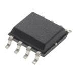
| 描述 | MOSFET N-CH 150V 3.5A 8-SOICMOSFET 150V 5A 3.1W |
| 产品分类 | FET - 单分离式半导体 |
| FET功能 | 标准 |
| FET类型 | MOSFET N 通道,金属氧化物 |
| Id-ContinuousDrainCurrent | 3.5 A |
| Id-连续漏极电流 | 3.5 A |
| 品牌 | Vishay SiliconixVishay / Siliconix |
| 产品手册 | |
| 产品图片 |
|
| rohs | RoHS 合规性豁免无铅 / 符合限制有害物质指令(RoHS)规范要求 |
| 产品系列 | 晶体管,MOSFET,Vishay / Siliconix SI4488DY-T1-E3TrenchFET® |
| 数据手册 | http://www.vishay.com/doc?71240 |
| 产品型号 | SI4488DY-T1-E3SI4488DY-T1-E3 |
| Pd-PowerDissipation | 1.56 W |
| Pd-功率耗散 | 1.56 W |
| RdsOn-Drain-SourceResistance | 50 mOhms |
| RdsOn-漏源导通电阻 | 50 mOhms |
| Vds-Drain-SourceBreakdownVoltage | 150 V |
| Vds-漏源极击穿电压 | 150 V |
| Vgs-Gate-SourceBreakdownVoltage | +/- 20 V |
| Vgs-栅源极击穿电压 | 20 V |
| 上升时间 | 7 ns |
| 下降时间 | 7 ns |
| 不同Id时的Vgs(th)(最大值) | 2V @ 250µA (最小) |
| 不同Vds时的输入电容(Ciss) | - |
| 不同Vgs时的栅极电荷(Qg) | 36nC @ 10V |
| 不同 Id、Vgs时的 RdsOn(最大值) | 50 毫欧 @ 5A,10V |
| 产品目录页面 | |
| 产品种类 | MOSFET |
| 供应商器件封装 | 8-SO |
| 其它名称 | SI4488DY-T1-E3TR |
| 典型关闭延迟时间 | 22 ns |
| 功率-最大值 | 1.56W |
| 包装 | 带卷 (TR) |
| 商标 | Vishay / Siliconix |
| 商标名 | TrenchFET |
| 安装类型 | 表面贴装 |
| 安装风格 | SMD/SMT |
| 封装 | Reel |
| 封装/外壳 | 8-SOIC(0.154",3.90mm 宽) |
| 封装/箱体 | SO-8 |
| 工厂包装数量 | 2500 |
| 晶体管极性 | N-Channel |
| 最大工作温度 | + 150 C |
| 最小工作温度 | - 55 C |
| 标准包装 | 2,500 |
| 漏源极电压(Vdss) | 150V |
| 电流-连续漏极(Id)(25°C时) | 3.5A (Ta) |
| 通道模式 | Enhancement |
| 配置 | Single |
| 零件号别名 | SI4488DY-E3 |


- 商务部:美国ITC正式对集成电路等产品启动337调查
- 曝三星4nm工艺存在良率问题 高通将骁龙8 Gen1或转产台积电
- 太阳诱电将投资9.5亿元在常州建新厂生产MLCC 预计2023年完工
- 英特尔发布欧洲新工厂建设计划 深化IDM 2.0 战略
- 台积电先进制程称霸业界 有大客户加持明年业绩稳了
- 达到5530亿美元!SIA预计今年全球半导体销售额将创下新高
- 英特尔拟将自动驾驶子公司Mobileye上市 估值或超500亿美元
- 三星加码芯片和SET,合并消费电子和移动部门,撤换高东真等 CEO
- 三星电子宣布重大人事变动 还合并消费电子和移动部门
- 海关总署:前11个月进口集成电路产品价值2.52万亿元 增长14.8%


PDF Datasheet 数据手册内容提取
Si4488DY Vishay Siliconix N-Channel 150-V (D-S) MOSFET FEATURES PRODUCT SUMMARY • Halogen-free According to IEC 61249-2-21 V (V) R (Ω) I (A) DS DS(on) D Definition 150 0.050 at VGS = 10 V 5.0 (cid:129) TrenchFET® Power MOSFETs (cid:129) Compliant to RoHS Directive 2002/95/EC D SO-8 S 1 8 D S 2 7 D G S 3 6 D G 4 5 D Top View S Ordering Information: Si4488DY-T1-E3 (Lead (Pb)-free) Si4488DY-T1-GE3 (Lead (Pb)-free and Halogen-free) N-Channel MOSFET ABSOLUTE MAXIMUM RATINGS T = 25 °C, unless otherwise noted A Parameter Symbol 10 s Steady State Unit Drain-Source Voltage VDS 150 V Gate-Source Voltage VGS ± 20 Continuous Drain Current (TJ = 150 °C)a TTAA == 2750 °°CC ID 54..00 32..58 Pulsed Drain Current IDM 50 A Avalanche Current L = 0.1 mH IAS 25 Continuous Source Current (Diode Conduction)a IS 2.8 1.4 TA = 25 °C 3.1 1.56 Maximum Power Dissipationa PD W TA = 70 °C 2.0 1.0 Operating Junction and Storage Temperature Range TJ, Tstg - 55 to 150 °C THERMAL RESISTANCE RATINGS Parameter Symbol Typical Maximum Unit t ≤ 10 s 33 40 Maximum Junction-to-Ambienta RthJA Steady State 65 80 °C/W Maximum Junction-to-Foot (Drain) Steady State RthJF 17 21 Notes: a. Surface Mounted on 1" x 1" FR4 board. Document Number: 71240 www.vishay.com S09-0705-Rev. C, 27-Apr-09 1
Si4488DY Vishay Siliconix SPECIFICATIONS T = 25 °C, unless otherwise noted J Parameter Symbol Test Conditions Min. Typ. Max. Unit Static Gate Threshold Voltage VGS(th) VDS = VGS, ID = 250 µA 2.0 V Gate-Body Leakage IGSS VDS = 0 V, VGS = ± 20 V ± 100 nA VDS = 120 V, VGS = 0 V 1 Zero Gate Voltage Drain Current IDSS µA VDS = 120 V, VGS = 0 V, TJ = 55 °C 5 On-State Drain Currenta ID(on) VDS ≥ 5 V, VGS = 10 V 50 A Drain-Source On-State Resistancea RDS(on) VGS = 10 V, ID = 5 A 0.041 0.050 Ω Forward Transconductancea gfs VDS = 15 V, ID = 5 A 18 S Diode Forward Voltagea VSD IS = 2.8 A, VGS = 0 V 0.75 1.1 V Dynamicb Total Gate Charge Qg 30 36 Gate-Source Charge Qgs VDS = 75 V, VGS = 10 V, ID = 5 A 8.5 nC Gate-Drain Charge Qgd 8.5 Gate Resistance Rg 0.2 0.85 1.2 Ω Turn-On Delay Time td(on) 12 18 Rise Time tr VDD = 75 V, RL = 15 Ω 7 11 Turn-Off Delay Time td(off) ID ≅ 5 A, VGEN = 10 V, Rg = 6 Ω 22 33 ns Fall Time tf 10 15 Source-Drain Reverse Recovery Time trr IF = 2.8 A, dI/dt = 100 A/µs 40 70 Notes: a. Pulse test; pulse width ≤ 300 µs, duty cycle ≤ 2 %. b. Guaranteed by design, not subject to production testing. Stresses beyond those listed under “Absolute Maximum Ratings” may cause permanent damage to the device. These are stress ratings only, and functional operation of the device at these or any other conditions beyond those indicated in the operational sections of the specifications is not implied. Exposure to absolute maximum rating conditions for extended periods may affect device reliability. TYPICAL CHARACTERISTICS 25°C, unless otherwise noted 50 50 VGS = 10 V thru 7 V 40 40 Current (A) 30 6 V urrent (A) 30 n C - DraiD 20 - Drain 20 TC = 125 °C I D I 10 10 5 V 25 °C - 55 °C 3, 4 V 0 0 0 2 4 6 8 10 0 1 2 3 4 5 6 7 VDS - Drain-to-Source Voltage (V) VGS - Gate-to-Source Voltage (V) Output Characteristics Transfer Characteristics www.vishay.com Document Number: 71240 2 S09-0705-Rev. C, 27-Apr-09
Si4488DY Vishay Siliconix TYPICAL CHARACTERISTICS 25°C, unless otherwise noted 0.10 3000 2500 0.08 F) p e ( 2000 c 0.06 an Ciss cit VGS = 10 V pa 1500 a C -on) 0.04 C - 1000 S( D R 0.02 500 Crss Coss 0.00 0 0 10 20 30 40 50 0 30 60 90 120 150 ID - Drain Current (A) VDS - Drain-to-Source Voltage (V) On-Resistance vs. Drain Current Capacitance 20 2.5 VDS = 75 V VGS = 10 V ID = 5 A ID = 5 A V) 16 2.0 ge ( e a c olt an e-to-Source V 182 - On-Resistn)(Normalized) 11..05 Gat S(o - RD S G 4 0.5 V 0 0.0 0 15 30 45 60 - 50 - 25 0 25 50 75 100 125 150 Qg - Total Gate Charge (nC) TJ - Junction Temperature (°C) Gate Charge On-Resistance vs. Junction Temperature 50 0.15 0.12 e Current (A) 10 TJ = 150 °C esistance ()Ω 0.09 ID = 5 A c R Sour On- 0.06 - IS TJ = 25 °C - S(on) D R 0.03 1 0.00 0.0 0.2 0.4 0.6 0.8 1.0 1.2 0 2 4 6 8 10 VSD - Source-to-Drain Voltage (V) VGS - Gate-to-Source Voltage (V) Source-Drain Diode Forward Voltage On-Resistance vs. Gate-to-Source Voltage Document Number: 71240 www.vishay.com S09-0705-Rev. C, 27-Apr-09 3
Si4488DY Vishay Siliconix TYPICAL CHARACTERISTICS 25°C, unless otherwise noted 1.0 100 0.5 ID = 250 µA e (V) (A) 10 T = 25 °C c 0.0 V n A a D ari I V S(th) -0.5 T = 125 °C VG 1 -1.0 -1.5 0.1 -50 -25 0 25 50 75 100 125 150 10-5 10-4 10-3 10-2 10-1 1 TJ - Temperature (°C) Time (s) Threshold Voltage Avalanche Current vs. Time 60 50 40 W) er ( 30 w o P 20 10 0 0.01 0.1 1 10 100 Time (s) Single Pulse Power 2 1 nt Duty Cycle = 0.5 e e Transiedance 0.2 ctivmp Notes: ed Effeermal I 0.1 0.1 PDM malizTh 0.05 t1 Nor 0.02 1. Duty Cyclet,2 D = t1 t2 2. Per Unit Base = RthJA = 65 °C/W 3. TJM - TA = PDMZthJA(t) Single Pulse 4. Surface Mounted 0.01 10-4 10-3 10-2 10-1 1 10 100 600 Square Wave Pulse Duration (s) Normalized Thermal Transient Impedance, Junction-to-Ambient www.vishay.com Document Number: 71240 4 S09-0705-Rev. C, 27-Apr-09
Si4488DY Vishay Siliconix TYPICAL CHARACTERISTICS 25°C, unless otherwise noted 2 1 nt Duty Cycle = 0.5 e e Transiedance 0.2 ctivmp zed Effehermal I 0.1 00..105 aliT m or 0.02 N Single Pulse 0.01 10-4 10-3 10-2 10-1 1 10 100 1000 Square Wave Pulse Duration (s) Normalized Thermal Transient Impedance, Junction-to-Foot Vishay Siliconix maintains worldwide manufacturing capability. Products may be manufactured at one of several qualified locations. Reliability data for Silicon Technology and Package Reliability represent a composite of all qualified locations. For related documents such as package/tape drawings, part marking, and reliability data, see www.vishay.com/ppg?71240. Document Number: 71240 www.vishay.com S09-0705-Rev. C, 27-Apr-09 5
Package Information Vishay Siliconix SOIC (NARROW): 8-LEAD JEDEC Part Number: MS-012 8 7 6 5 E H 1 2 3 4 S D h x 45 C 0.25 mm (Gage Plane) A All Leads q 0.101 mm e B A1 L 0.004" MILLIMETERS INCHES DIM Min Max Min Max A 1.35 1.75 0.053 0.069 A 0.10 0.20 0.004 0.008 1 B 0.35 0.51 0.014 0.020 C 0.19 0.25 0.0075 0.010 D 4.80 5.00 0.189 0.196 E 3.80 4.00 0.150 0.157 e 1.27 BSC 0.050 BSC H 5.80 6.20 0.228 0.244 h 0.25 0.50 0.010 0.020 L 0.50 0.93 0.020 0.037 q 0° 8° 0° 8° S 0.44 0.64 0.018 0.026 ECN: C-06527-Rev. I, 11-Sep-06 DWG: 5498 Document Number: 71192 www.vishay.com 11-Sep-06 1
Application Note 826 Vishay Siliconix RECOMMENDED MINIMUM PADS FOR SO-8 0.172 (4.369) 0.028 (0.711) 6 8) 2 1) 4 4 5 6 2 2 1 8 0. 6. 0. 3. ( ( 7 4) 4 9 0 1 0. 1. ( 0.022 0.050 (0.559) (1.270) Recommended Minimum Pads Dimensions in Inches/(mm) Return to Index Return to Index E T O N N O I T A C I L P P A www.vishay.com Document Number: 72606 22 Revision: 21-Jan-08
Legal Disclaimer Notice www.vishay.com Vishay Disclaimer ALL PRODUCT, PRODUCT SPECIFICATIONS AND DATA ARE SUBJECT TO CHANGE WITHOUT NOTICE TO IMPROVE RELIABILITY, FUNCTION OR DESIGN OR OTHERWISE. Vishay Intertechnology, Inc., its affiliates, agents, and employees, and all persons acting on its or their behalf (collectively, “Vishay”), disclaim any and all liability for any errors, inaccuracies or incompleteness contained in any datasheet or in any other disclosure relating to any product. Vishay makes no warranty, representation or guarantee regarding the suitability of the products for any particular purpose or the continuing production of any product. To the maximum extent permitted by applicable law, Vishay disclaims (i) any and all liability arising out of the application or use of any product, (ii) any and all liability, including without limitation special, consequential or incidental damages, and (iii) any and all implied warranties, including warranties of fitness for particular purpose, non-infringement and merchantability. Statements regarding the suitability of products for certain types of applications are based on Vishay’s knowledge of typical requirements that are often placed on Vishay products in generic applications. Such statements are not binding statements about the suitability of products for a particular application. It is the customer’s responsibility to validate that a particular product with the properties described in the product specification is suitable for use in a particular application. Parameters provided in datasheets and / or specifications may vary in different applications and performance may vary over time. All operating parameters, including typical parameters, must be validated for each customer application by the customer’s technical experts. Product specifications do not expand or otherwise modify Vishay’s terms and conditions of purchase, including but not limited to the warranty expressed therein. Except as expressly indicated in writing, Vishay products are not designed for use in medical, life-saving, or life-sustaining applications or for any other application in which the failure of the Vishay product could result in personal injury or death. Customers using or selling Vishay products not expressly indicated for use in such applications do so at their own risk. Please contact authorized Vishay personnel to obtain written terms and conditions regarding products designed for such applications. No license, express or implied, by estoppel or otherwise, to any intellectual property rights is granted by this document or by any conduct of Vishay. Product names and markings noted herein may be trademarks of their respective owners. © 2017 VISHAY INTERTECHNOLOGY, INC. ALL RIGHTS RESERVED Revision: 08-Feb-17 1 Document Number: 91000
Mouser Electronics Authorized Distributor Click to View Pricing, Inventory, Delivery & Lifecycle Information: V ishay: SI4488DY-T1 SI4488DY-T1-GE3 SI4488DY-T1-E3 SI4488DY-E3 SI4488DY