ICGOO在线商城 > 分立半导体产品 > 晶体管 - FET,MOSFET - 单 > SI4124DY-T1-GE3
 Datasheet下载
- 型号: SI4124DY-T1-GE3
- 制造商: Vishay
- 库位|库存: xxxx|xxxx
- 要求:
| 数量阶梯 | 香港交货 | 国内含税 |
| +xxxx | $xxxx | ¥xxxx |
查看当月历史价格
查看今年历史价格
SI4124DY-T1-GE3产品简介:
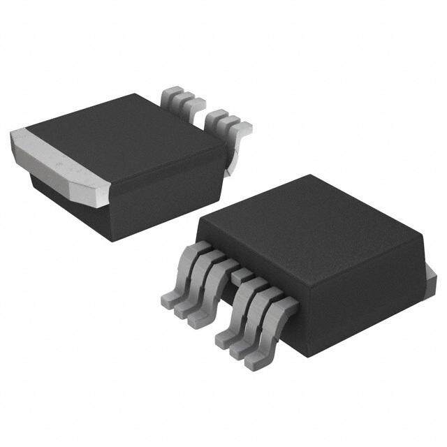
ICGOO电子元器件商城为您提供SI4124DY-T1-GE3由Vishay设计生产,在icgoo商城现货销售,并且可以通过原厂、代理商等渠道进行代购。 SI4124DY-T1-GE3价格参考。VishaySI4124DY-T1-GE3封装/规格:晶体管 - FET,MOSFET - 单, 表面贴装 N 沟道 40V 20.5A(Tc) 2.5W(Ta),5.7W(Tc) 8-SO。您可以下载SI4124DY-T1-GE3参考资料、Datasheet数据手册功能说明书,资料中有SI4124DY-T1-GE3 详细功能的应用电路图电压和使用方法及教程。
| 参数 | 数值 |
| 产品目录 | |
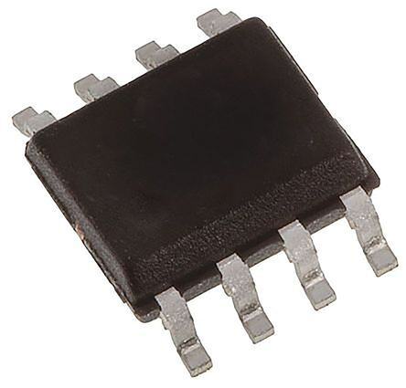
| 描述 | MOSFET N-CH 40V 20.5A 8-SOIC |
| 产品分类 | FET - 单 |
| FET功能 | 标准 |
| FET类型 | MOSFET N 通道,金属氧化物 |
| 品牌 | Vishay Siliconix |
| 数据手册 | |
| 产品图片 |
|
| 产品型号 | SI4124DY-T1-GE3 |
| rohs | 无铅 / 符合限制有害物质指令(RoHS)规范要求 |
| 产品系列 | TrenchFET® |
| 不同Id时的Vgs(th)(最大值) | 3V @ 250µA |
| 不同Vds时的输入电容(Ciss) | 3540pF @ 20V |
| 不同Vgs时的栅极电荷(Qg) | 77nC @ 10V |
| 不同 Id、Vgs时的 RdsOn(最大值) | 7.5 毫欧 @ 14A,10V |
| 供应商器件封装 | 8-SO |
| 其它名称 | SI4124DY-T1-GE3DKR |
| 功率-最大值 | 5.7W |
| 包装 | Digi-Reel® |
| 安装类型 | 表面贴装 |
| 封装/外壳 | 8-SOIC(0.154",3.90mm 宽) |
| 标准包装 | 1 |
| 漏源极电压(Vdss) | 40V |
| 电流-连续漏极(Id)(25°C时) | 20.5A (Tc) |


- 商务部:美国ITC正式对集成电路等产品启动337调查
- 曝三星4nm工艺存在良率问题 高通将骁龙8 Gen1或转产台积电
- 太阳诱电将投资9.5亿元在常州建新厂生产MLCC 预计2023年完工
- 英特尔发布欧洲新工厂建设计划 深化IDM 2.0 战略
- 台积电先进制程称霸业界 有大客户加持明年业绩稳了
- 达到5530亿美元!SIA预计今年全球半导体销售额将创下新高
- 英特尔拟将自动驾驶子公司Mobileye上市 估值或超500亿美元
- 三星加码芯片和SET,合并消费电子和移动部门,撤换高东真等 CEO
- 三星电子宣布重大人事变动 还合并消费电子和移动部门
- 海关总署:前11个月进口集成电路产品价值2.52万亿元 增长14.8%


PDF Datasheet 数据手册内容提取
New Product Si4124DY Vishay Siliconix N-Channel 40-V (D-S) MOSFET FEATURES PRODUCT SUMMARY • Halogen-free According to IEC 61249-2-21 VDS (V) RDS(on) (Ω) ID (A)d Qg (Typ.) Available 0.0075 at VGS = 10 V 20.5 (cid:129) TrenchFET® Power MOSFET 40 21 nC (cid:129) 100 % R Tested 0.009 at VGS = 4.5 V 18.7 g APPLICATIONS (cid:129) Synchronous Rectification SO-8 (cid:129) DC/DC D S 1 8 D S 2 7 D S 3 6 D G 4 5 D G Top View S Ordering Information: Si4124DY-T1-E3 (Lead (Pb)-free) Si4124DY-T1-GE3 (Lead (Pb)-free and Halogen-free) N-Channel MOSFET ABSOLUTE MAXIMUM RATINGS T = 25 °C, unless otherwise noted A Parameter Symbol Limit Unit Drain-Source Voltage V 40 DS V Gate-Source Voltage V ± 20 GS T = 25 °C 20.5 C T = 70 °C 16.4 C Continuous Drain Current (T = 150 °C) I J T = 25 °C D 13.6a, b A A T = 70 °C 10.9a, b A Pulsed Drain Current I 50 DM Avalanche Current I 33 AS L = 0.1 mH Avalanche Energy E 54 mJ AS T = 25 °C 4.7 C Continuous Source-Drain Diode Current I A T = 25 °C S 2.1a, b A T = 25 °C 5.7 C T = 70 °C 3.6 C Maximum Power Dissipation P W T = 25 °C D 2.5a, b A T = 70 °C 1.6a, b A Operating Junction and Storage Temperature Range T , T - 55 to 150 °C J stg THERMAL RESISTANCE RATINGS Parameter Symbol Typical Maximum Unit Maximum Junction-to-Ambienta, c t ≤ 10 s R 39 50 thJA °C/W Maximum Junction-to-Foot (Drain) Steady State R 18 22 thJF Notes: a. Surface Mounted on 1" x 1" FR4 board. b. t = 10 s. c. Maximum under Steady State conditions is 85 °C/W. d. Based on T = 25 °C. C Document Number: 68601 www.vishay.com S09-0392-Rev. B, 09-Mar-09 1
New Product Si4124DY Vishay Siliconix SPECIFICATIONS T = 25 °C, unless otherwise noted J Parameter Symbol Test Conditions Min. Typ. Max. Unit Static Drain-Source Breakdown Voltage VDS VGS = 0 V, ID = 250 µA 40 V VDS Temperature Coefficient ΔVDS/TJ ID = 250 µA 46 mV/°C VGS(th) Temperature Coefficient ΔVGS(th)/TJ - 6.7 Gate-Source Threshold Voltage VGS(th) VDS = VGS , ID = 250 µA 1 3 V Gate-Source Leakage IGSS VDS = 0 V, VGS = ± 20 V ± 100 nA VDS = 40 V, VGS = 0 V 1 Zero Gate Voltage Drain Current IDSS µA VDS = 40 V, VGS = 0 V, TJ = 55 °C 5 On-State Drain Currenta ID(on) VDS ≥ 5 V, VGS = 10 V 50 A Drain-Source On-State Resistancea RDS(on) VGS = 10 V, ID = 14 A 0.0062 0.0075 Ω VGS = 4.5 V, ID = 12 A 0.0073 0.009 Forward Transconductancea gfs VDS = 15 V, ID = 16 A 55 S Dynamicb Input Capacitance Ciss 3540 Output Capacitance Coss VDS = 20 V, VGS = 0 V, f = 1 MHz 335 pF Reverse Transfer Capacitance Crss 142 Total Gate Charge Qg VDS = 10 V, VGS = 10 V, ID = 16 A 51 77 21 32 nC Gate-Source Charge Qgs VDS = 10 V, VGS = 4.5 V, ID = 16 A 10.7 Gate-Drain Charge Qgd 3.0 Gate Resistance Rg f = 1 MHz 0.75 1.5 Ω Turn-on Delay Time td(on) 30 45 Rise Time tr VDD = 20 V, RL = 2 Ω 14 21 Turn-Off Delay Time td(off) ID ≅ 10 A, VGEN = 4.5 V, Rg = 1 Ω 38 60 Fall Time tf 11 17 ns Turn-on Delay Time td(on) 14 21 Rise Time tr VDD = 20 V, RL = 2 Ω 10 15 Turn-Off Delay Time td(off) ID ≅ 10 A, VGEN = 10 V, Rg = 1 Ω 32 50 Fall Time tf 8 15 Drain-Source Body Diode Characteristics Continuous Source-Drain Diode Current IS TC = 25 °C 32 A Pulse Diode Forward Current ISM 50 Body Diode Voltage VSD IS = 10 A, VGS = 0 V 0.8 1.2 V Body Diode Reverse Recovery Time trr 25 50 ns Body Diode Reverse Recovery Charge Qrr 19 38 nC I = 10 A, dI/dt = 100 A/µs, T = 25 °C F J Reverse Recovery Fall Time ta 13 ns Reverse Recovery Rise Time tb 12 Notes: a. Pulse test; pulse width ≤ 300 µs, duty cycle ≤ 2 %. b. Guaranteed by design, not subject to production testing. Stresses beyond those listed under “Absolute Maximum Ratings” may cause permanent damage to the device. These are stress ratings only, and functional operation of the device at these or any other conditions beyond those indicated in the operational sections of the specifications is not implied. Exposure to absolute maximum rating conditions for extended periods may affect device reliability. www.vishay.com Document Number: 68601 2 S09-0392-Rev. B, 09-Mar-09
New Product Si4124DY Vishay Siliconix TYPICAL CHARACTERISTICS 25°C, unless otherwise noted 50 10 V = 10 V thru 4 V GS 40 8 A) A) nt ( 30 nt ( 6 e e Curr VGS=3V Curr n n Drai 20 Drai 4 - D - D TC=125 °C I I 10 2 TC=25 °C TC=- 55 °C 0 0 0.0 0.5 1.0 1.5 2.0 0 1 2 3 4 V - Drain-to-Source Voltage (V) V - Gate-to-Source Voltage (V) DS GS Output Characteristics Transfer Characteristics 0.010 4000 C iss 0.008 VGS=4.5V 3200 Ω) nce ( pF) sista 0.006 VGS=10V nce ( 2400 e a n-R acit - OS(on) 0.004 C - Cap 1600 D R 0.002 800 Coss C rss 0.000 0 0 10 20 30 40 50 0 10 20 30 40 ID - Drain Current (A) VDS - Drain-to-Source Voltage (V) On-Resistance vs. Drain Current and Gate Voltage Capacitance 10 2.0 ID=16A VDS=10 V ID=14A VGS=10V V) 8 ate-to-Source Voltage ( 46 VDS=20V VDS=30 V - On-ResistanceS(on)(Normalized) 11..26 VGS=4.5V G D - GS 2 R 0.8 V 0 0.4 0 11 22 33 44 55 - 50 - 25 0 25 50 75 100 125 150 Q - Total Gate Charge (nC) T - Junction Temperature (°C) g J Gate Charge On-Resistance vs. Junction Temperature Document Number: 68601 www.vishay.com S09-0392-Rev. B, 09-Mar-09 3
New Product Si4124DY Vishay Siliconix TYPICAL CHARACTERISTICS 25°C, unless otherwise noted 100 0.03 T = 150 °C ID=14A J 10 Ω) Current (A) 1 TJ = 25 °C esistance ( 0.02 I - Source S 0.1 - On-RDS(on) 0.01 TJ=125 °C R 0.01 TJ=25 °C 0.001 0.00 0.0 0.2 0.4 0.6 0.8 1.0 1.2 0 1 2 3 4 5 6 7 8 9 10 V - Source-to-Drain Voltage (V) V - Gate-to-Source Voltage (V) SD GS Source-Drain Diode Forward Voltage On-Resistance vs. Gate-to-Source Voltage 0.6 170 0.3 ID=250 µA 136 V) nce ( 0.0 ID=5mA W) 102 - VariaS(th) - 0.3 Power ( 68 G V - 0.6 34 - 0.9 0 - 50 - 25 0 25 50 75 100 125 150 0.001 0.01 0.1 1 10 T - Junction Temperature (°C) Time (s) J Threshold Voltage Single Pulse Power (Junction-to-Ambient) 100 Limited by R * DS(on) 100 µs 10 A) nt ( 1 ms e Curr 1 10 ms n ai Dr 100 ms I - D 1 s 0.1 10 s T = 25 °C 100 s, DC A BVDSS Single Pulse Limited 0.01 0.1 1 10 100 V - Drain-to-Source Voltage (V) DS * V > minimum V at which R is specified DS GS DS(on) Safe Operating Area, Junction-to-Ambient www.vishay.com Document Number: 68601 4 S09-0392-Rev. B, 09-Mar-09
New Product Si4124DY Vishay Siliconix TYPICAL CHARACTERISTICS 25°C, unless otherwise noted 25 20 A) ent ( 15 urr C n Drai 10 - D I 5 0 0 25 50 75 100 125 150 T - Case Temperature (°C) C Current Derating*, Junction-to-Foot 7.0 1.80 5.6 1.44 W) 4.2 W) 1.08 er ( er ( w w Po 2.8 Po 0.72 1.4 0.36 0.0 0.00 0 25 50 75 100 125 150 0 25 50 75 100 125 150 TC - Case Temperature (°C) TA - Ambient Temperature (°C) Power Derating, Junction-to-Foot Power Derating, Junction-to-Ambient * The power dissipation P is based on T = 150 °C, using junction-to-case thermal resistance, and is more useful in settling the upper D J(max) dissipation limit for cases where additional heatsinking is used. It is used to determine the current rating, when this rating falls below the package limit. Document Number: 68601 www.vishay.com S09-0392-Rev. B, 09-Mar-09 5
New Product Si4124DY Vishay Siliconix TYPICAL CHARACTERISTICS 25°C, unless otherwise noted 1 Duty Cycle = 0.5 nt e Transiance 0.2 ctive mped 0.1 Notes: ed Effeermal I 0.1 0.05 PDM zh maliT t1 Nor 0.02 1. Duty Cyclet,2 D = t1 t2 2. Per Unit Base = RthJA = 85 °C/W 3. TJM - TA = PDMZthJA(t) 0.01 Single Pulse 4. Surface Mounted 10-1 10-3 10-2 10-1 1 10 100 1000 Square Wave Pulse Duration (s) Normalized Thermal Transient Impedance, Junction-to-Ambient 1 Duty Cycle = 0.5 nt e Transiance 0.2 ctive mped 0.1 ed Effeermal I 0.1 0.05 zh aliT m or N 0.02 Single Pulse 0.01 10-4 10-3 10-2 10-1 1 10 Square Wave Pulse Duration (s) Normalized Thermal Transient Impedance, Junction-to-Foot Vishay Siliconix maintains worldwide manufacturing capability. Products may be manufactured at one of several qualified locations. Reliability data for Silicon Technology and Package Reliability represent a composite of all qualified locations. For related documents such as package/tape drawings, part marking, and reliability data, see www.vishay.com/ppg?68601. www.vishay.com Document Number: 68601 6 S09-0392-Rev. B, 09-Mar-09
Package Information Vishay Siliconix SOIC (NARROW): 8-LEAD JEDEC Part Number: MS-012 8 7 6 5 E H 1 2 3 4 S D h x 45 C 0.25 mm (Gage Plane) A All Leads q 0.101 mm e B A1 L 0.004" MILLIMETERS INCHES DIM Min Max Min Max A 1.35 1.75 0.053 0.069 A 0.10 0.20 0.004 0.008 1 B 0.35 0.51 0.014 0.020 C 0.19 0.25 0.0075 0.010 D 4.80 5.00 0.189 0.196 E 3.80 4.00 0.150 0.157 e 1.27 BSC 0.050 BSC H 5.80 6.20 0.228 0.244 h 0.25 0.50 0.010 0.020 L 0.50 0.93 0.020 0.037 q 0° 8° 0° 8° S 0.44 0.64 0.018 0.026 ECN: C-06527-Rev. I, 11-Sep-06 DWG: 5498 Document Number: 71192 www.vishay.com 11-Sep-06 1
Application Note 826 Vishay Siliconix RECOMMENDED MINIMUM PADS FOR SO-8 0.172 (4.369) 0.028 (0.711) 6 8) 2 1) 4 4 5 6 2 2 1 8 0. 6. 0. 3. ( ( 7 4) 4 9 0 1 0. 1. ( 0.022 0.050 (0.559) (1.270) Recommended Minimum Pads Dimensions in Inches/(mm) Return to Index Return to Index E T O N N O I T A C I L P P A www.vishay.com Document Number: 72606 22 Revision: 21-Jan-08
Legal Disclaimer Notice www.vishay.com Vishay Disclaimer ALL PRODUCT, PRODUCT SPECIFICATIONS AND DATA ARE SUBJECT TO CHANGE WITHOUT NOTICE TO IMPROVE RELIABILITY, FUNCTION OR DESIGN OR OTHERWISE. Vishay Intertechnology, Inc., its affiliates, agents, and employees, and all persons acting on its or their behalf (collectively, “Vishay”), disclaim any and all liability for any errors, inaccuracies or incompleteness contained in any datasheet or in any other disclosure relating to any product. Vishay makes no warranty, representation or guarantee regarding the suitability of the products for any particular purpose or the continuing production of any product. To the maximum extent permitted by applicable law, Vishay disclaims (i) any and all liability arising out of the application or use of any product, (ii) any and all liability, including without limitation special, consequential or incidental damages, and (iii) any and all implied warranties, including warranties of fitness for particular purpose, non-infringement and merchantability. Statements regarding the suitability of products for certain types of applications are based on Vishay’s knowledge of typical requirements that are often placed on Vishay products in generic applications. Such statements are not binding statements about the suitability of products for a particular application. It is the customer’s responsibility to validate that a particular product with the properties described in the product specification is suitable for use in a particular application. Parameters provided in datasheets and / or specifications may vary in different applications and performance may vary over time. All operating parameters, including typical parameters, must be validated for each customer application by the customer’s technical experts. Product specifications do not expand or otherwise modify Vishay’s terms and conditions of purchase, including but not limited to the warranty expressed therein. Except as expressly indicated in writing, Vishay products are not designed for use in medical, life-saving, or life-sustaining applications or for any other application in which the failure of the Vishay product could result in personal injury or death. Customers using or selling Vishay products not expressly indicated for use in such applications do so at their own risk. Please contact authorized Vishay personnel to obtain written terms and conditions regarding products designed for such applications. No license, express or implied, by estoppel or otherwise, to any intellectual property rights is granted by this document or by any conduct of Vishay. Product names and markings noted herein may be trademarks of their respective owners. © 2017 VISHAY INTERTECHNOLOGY, INC. ALL RIGHTS RESERVED Revision: 08-Feb-17 1 Document Number: 91000
Mouser Electronics Authorized Distributor Click to View Pricing, Inventory, Delivery & Lifecycle Information: V ishay: SI4124DY-T1-E3 SI4124DY-T1-GE3