ICGOO在线商城 > 分立半导体产品 > 晶体管 - FET,MOSFET - 单 > SI2334DS-T1-GE3

 Datasheet下载
- 型号: SI2334DS-T1-GE3
- 制造商: Vishay
- 库位|库存: xxxx|xxxx
- 要求:
| 数量阶梯 | 香港交货 | 国内含税 |
| +xxxx | $xxxx | ¥xxxx |
查看当月历史价格
查看今年历史价格
SI2334DS-T1-GE3产品简介:
ICGOO电子元器件商城为您提供SI2334DS-T1-GE3由Vishay设计生产,在icgoo商城现货销售,并且可以通过原厂、代理商等渠道进行代购。 SI2334DS-T1-GE3价格参考。VishaySI2334DS-T1-GE3封装/规格:晶体管 - FET,MOSFET - 单, 表面贴装 N 沟道 30V 4.9A(Tc) 1.3W(Ta),1.7W(Tc) SOT-23-3(TO-236)。您可以下载SI2334DS-T1-GE3参考资料、Datasheet数据手册功能说明书,资料中有SI2334DS-T1-GE3 详细功能的应用电路图电压和使用方法及教程。
| 参数 | 数值 |
| 产品目录 | |
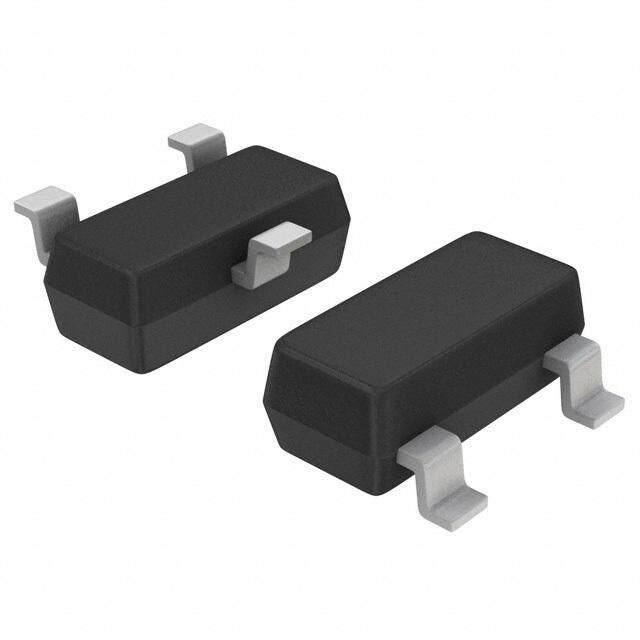
| 描述 | MOSFET N-CH 30V 4.9A SOT-23 |
| 产品分类 | FET - 单 |
| FET功能 | 逻辑电平门 |
| FET类型 | MOSFET N 通道,金属氧化物 |
| 品牌 | Vishay Siliconix |
| 数据手册 | |
| 产品图片 |
|
| 产品型号 | SI2334DS-T1-GE3 |
| rohs | 无铅 / 符合限制有害物质指令(RoHS)规范要求 |
| 产品系列 | TrenchFET® |
| 不同Id时的Vgs(th)(最大值) | 1V @ 250µA |
| 不同Vds时的输入电容(Ciss) | 634pF @ 15V |
| 不同Vgs时的栅极电荷(Qg) | 10nC @ 4.5V |
| 不同 Id、Vgs时的 RdsOn(最大值) | 44 毫欧 @ 4.2A,4.5V |
| 供应商器件封装 | SOT-23-3(TO-236) |
| 其它名称 | SI2334DS-T1-GE3TR |
| 功率-最大值 | 1.7W |
| 包装 | 带卷 (TR) |
| 安装类型 | 表面贴装 |
| 封装/外壳 | TO-236-3,SC-59,SOT-23-3 |
| 标准包装 | 3,000 |
| 漏源极电压(Vdss) | 30V |
| 电流-连续漏极(Id)(25°C时) | 4.9A (Tc) |


PDF Datasheet 数据手册内容提取
New Product Si2334DS Vishay Siliconix N-Channel 30 V (D-S) MOSFET FEATURES PRODUCT SUMMARY • Halogen-free According to IEC 61249-2-21 V (V) R () I (A)a Q (Typ.) DS DS(on) D g Definition 0.044 at VGS = 4.5 V 4.9 (cid:129) TrenchFET® Power MOSFET 30 3.7 nC 0.050 at VGS = 2.5 V 4.6 (cid:129) 100 % Rg Tested (cid:129) Compliant to RoHS Directive 2002/95/EC APPLICATIONS (cid:129) DC/DC Converter for Portable Devices TO-236 (cid:129) Load Switch (SOT-23) D G 1 3 D S 2 G Top View Si2334DS (PS)* * Marking Code S Ordering Information: Si2334DS-T1-GE3 (Lead (Pb)-free and Halogen-free) N-Channel MOSFET ABSOLUTE MAXIMUM RATINGS T = 25 °C, unless otherwise noted A Parameter Symbol Limit Unit Drain-Source Voltage V 30 DS V Gate-Source Voltage V ± 8 GS T = 25 °C 4.9 C T = 70 °C 3.9 C Continuous Drain Current (T = 150 °C) I J T = 25 °C D 4.2b, c A T = 70 °C 3.4b, c A A Pulsed Drain Current I 10 DM T = 25 °C 1.4 C Continuous Source-Drain Diode Current I T = 25 °C S 1.1b, c A T = 25 °C 1.7 C T = 70 °C 1.1 C Maximum Power Dissipation P W T = 25 °C D 1.3b, c A T = 70 °C 0.8b, c A Operating Junction and Storage Temperature Range TJ, Tstg - 55 to 150 °C THERMAL RESISTANCE RATINGS Parameter Symbol Typical Maximum Unit Maximum Junction-to-Ambientb, d t 5 s RthJA 80 100 °C/W Maximum Junction-to-Foot (Drain) Steady State R 60 75 thJF Notes: a. Based on T = 25 °C. C b. Surface mounted on 1" x 1" FR4 board. c. t = 5 s. d. Maximum under steady state conditions is 166 °C/W. Document Number: 66802 www.vishay.com S10-1533-Rev. A, 19-Jul-10 1
New Product Si2334DS Vishay Siliconix SPECIFICATIONS T = 25 °C, unless otherwise noted J Parameter Symbol Test Conditions Min. Typ. Max. Unit Static Drain-Source Breakdown Voltage VDS VGS = 0 V, ID = 250 µA 30 V VDS Temperature Coefficient VDS/TJ 2.8 ID = 250 µA mV/°C VGS(th) Temperature Coefficient VGS(th)/TJ - 0.2 Gate-Source Threshold Voltage VGS(th) VDS = VGS , ID = 250 µA 0.4 1.0 V Gate-Source Leakage IGSS VDS = 0 V, VGS = ± 8 V ± 100 nA VDS = 30 V, VGS = 0 V 1 Zero Gate Voltage Drain Current IDSS µA VDS = 30 V, VGS = 0 V, TJ = 55 °C 10 On-State Drain Currenta ID(on) VDS 5 V, VGS = 10 V 10 A VGS 4.5 V, ID = 4.2 A 0.035 0.044 Drain-Source On-State Resistancea RDS(on) VGS 2.5 V, ID = 4.0 A 0.040 0.050 Forward Transconductancea gfs VDS = 15 V, ID = 4.2 A 27 S Dynamicb Input Capacitance Ciss 634 Output Capacitance Coss VDS = 15 V, VGS = 0 V, f = 1 MHz 65 pF Reverse Transfer Capacitance Crss 30 Total Gate Charge Qg VDS = 15 V, VGS = 4.5 V, ID = 4.2 A 6.5 10 3.7 6 nC Gate-Source Charge Qgs VDS = 15 V, VGS = 2.5 V, ID = 4.2 A 1.2 Gate-Drain Charge Qgd 0.8 Gate Resistance Rg f = 1 MHz 0.5 2.7 5.4 Turn-On Delay Time td(on) 6 12 Rise Time tr VDD = 15 V, RL = 4.4 10 20 Turn-Off Delay Time td(off) ID 3.4 A, VGEN = 4.5 V, Rg = 1 16 24 Fall Time tf 8 16 ns Turn-On Delay Time td(on) 4 8 Rise Time tr VDD = 15 V, RL = 4.4 10 20 Turn-Off Delay Time td(off) ID 3.4 A, VGEN = 8 V, Rg = 1 18 27 Fall Time tf 8 16 Drain-Source Body Diode Characteristics Continuous Source-Drain Diode Current IS TC = 25 °C 1.4 A Pulse Diode Forward Current ISM 10 Body Diode Voltage VSD IS = 3.4 A, VGS 0 V 0.8 1.2 V Body Diode Reverse Recovery Time trr 11 20 ns Body Diode Reverse Recovery Charge Qrr 5 10 nC I = 3.4 A, dI/dt = 100 A/µs, T = 25 °C F J Reverse Recovery Fall Time ta 7 ns Reverse Recovery Rise Time tb 4 Notes: a. Pulse test; pulse width 300 µs, duty cycle 2 %. b. Guaranteed by design, not subject to production testing. Stresses beyond those listed under “Absolute Maximum Ratings” may cause permanent damage to the device. These are stress ratings only, and functional operation of the device at these or any other conditions beyond those indicated in the operational sections of the specifications is not implied. Exposure to absolute maximum rating conditions for extended periods may affect device reliability. www.vishay.com Document Number: 66802 2 S10-1533-Rev. A, 19-Jul-10
New Product Si2334DS Vishay Siliconix TYPICAL CHARACTERISTICS 25 °C, unless otherwise noted 10 5 VGS=5Vthru1.5V 8 4 A) A) ent ( 6 ent ( 3 Curr Curr TC=25 °C n n Drai 4 Drai 2 I- D I - D 2 1 VGS=1V TC=125 °C TC=-55 °C 0 0 0.0 0.5 1.0 1.5 2.0 0.0 0.3 0.6 0.9 1.2 1.5 V - Drain-to-Source Voltage (V) V - Gate-to-Source Voltage (V) DS GS Output Characteristics Transfer Characteristics 0.050 880 Ω) 0.045 660 Ciss stance ( 0.040 VGS=2.5V ce (pF) - On-ResiS(on) 0.035 VGS=4.5V C - Capacitan 440 RD 220 0.030 Coss 0.025 0 Crss 0 2 4 6 8 10 0 6 12 18 24 30 ID - Drain Current (A) VDS - Drain-to-Source Voltage (V) On-Resistance vs. Drain Current Capacitance 4.5 1.85 ge (V) ID=4.2A VDS=15V e 1.60 VGS=2.5V;ID=4A a c olt 3.0 an ate-to-Source V 1.5 VDS=8V VDS=24V - On-ResistS(on)(Normalized) 11..1305 VGS=4.5V;ID=4.2A G D - GS R 0.85 V 0 0.60 0 2 4 6 8 - 50 - 25 0 25 50 75 100 125 150 Q - Total Gate Charge (nC) T - Junction Temperature (°C) g J Gate Charge On-Resistance vs. Junction Temperature Document Number: 66802 www.vishay.com S10-1533-Rev. A, 19-Jul-10 3
New Product Si2334DS Vishay Siliconix TYPICAL CHARACTERISTICS 25°C, unless otherwise noted 100 0.080 ID=4.2A Ω) 0.065 nt (A) 10 TJ=150 °C nce ( e a e Curr Resist 0.050 TJ=125 °C I - SourcS 1 TJ=25 °C R - On-DS(on) 0.035 TJ=25 °C 0.1 0.020 0 0.3 0.6 0.9 1.2 0 2 4 6 8 V - Source-to-Drain Voltage (V) V - Gate-to-Source Voltage (V) SD GS Source-Drain Diode Forward Voltage On-Resistance vs. Gate-to-Source Voltage 0.8 24 0.7 18 V) 0.6 W) (S(th) ID=250 μA wer ( 12 VG 0.5 Po 6 0.4 0.3 0 - 50 - 25 0 25 50 75 100 125 150 0.001 0.01 0.1 1 10 100 T - Temperature (°C) Time (s) J Threshold Voltage Single Pulse Power 100 LimitedbyRDS(on)* 10 A) nt ( 100μs e urr C 1 n 1ms ai Dr - D 10ms I 0.1 TA=25 °C SinglePulse 100ms 1s,10s BVDSSLimited DC 0.01 0.1 1 10 100 V - Drain-to-Source Voltage (V) DS * V > minimum V at which R is specified GS GS DS(on) Safe Operating Area, Junction-to-Ambient www.vishay.com Document Number: 66802 4 S10-1533-Rev. A, 19-Jul-10
New Product Si2334DS Vishay Siliconix TYPICAL CHARACTERISTICS 25°C, unless otherwise noted 6.0 4.5 A) nt ( e urr C 3.0 n ai Dr - D I 1.5 0 0 25 50 75 100 125 150 T - Case Temperature (°C) C Current Derating* 2.0 1.0 0.8 1.5 W) W) 0.6 wer ( 1.0 wer ( Po Po 0.4 0.5 0.2 0 0 0 25 50 75 100 125 150 0 25 50 75 100 125 150 TC - Case Temperature (°C) TA - Ambient Temperature (°C) Power, Junction-to-Foot Power, Junction-to-Ambient * The power dissipation P is based on T = 150 °C, using junction-to-case thermal resistance, and is more useful in settling the upper D J(max) dissipation limit for cases where additional heatsinking is used. It is used to determine the current rating, when this rating falls below the package limit. Document Number: 66802 www.vishay.com S10-1533-Rev. A, 19-Jul-10 5
New Product Si2334DS Vishay Siliconix TYPICAL CHARACTERISTICS 25 °C, unless otherwise noted 1 DutyCycle=0.5 nt e Transiance 0.2 ctivemped 0.1 Notes: edEffeermalI 0.1 0.05 PDM zh maliT t1 Nor 0.02 1.DutyCyclet,2D= t1 t2 2.PerUnitBase=RthJA=166 °C/W 3.TJM-TA=PDMZthJA(t) SinglePulse 4.SurfaceMounted 0.01 10-4 10-3 10-2 10-1 1 10 100 1000 SquareWavePulseDuration(s) Normalized Thermal Transient Impedance, Junction-to-Ambient 1 DutyCycle=0.5 nt e Transiance 0.2 ctivemped 0.1 EffemalI 0.1 eder 0.05 zh aliT m or 0.02 N SinglePulse 0.01 10-4 10-3 10-2 10-1 1 SquareWavePulseDuration(s) Normalized Thermal Transient Impedance, Junction-to-Foot Vishay Siliconix maintains worldwide manufacturing capability. Products may be manufactured at one of several qualified locations. Reliability data for Silicon Technology and Package Reliability represent a composite of all qualified locations. For related documents such as package/tape drawings, part marking, and reliability data, see www.vishay.com/ppg?66802. www.vishay.com Document Number: 66802 6 S10-1533-Rev. A, 19-Jul-10
Package Information Vishay Siliconix SOT-23 (TO-236): 3-LEAD b 3 E1 E 1 2 e S e1 D 0.10 mm C A A2 0.004" C q 0.25 mm Gauge Plane Seating Plane Seating Plane A1 C L L1 MILLIMETERS INCHES Dim Min Max Min Max A 0.89 1.12 0.035 0.044 A1 0.01 0.10 0.0004 0.004 A2 0.88 1.02 0.0346 0.040 b 0.35 0.50 0.014 0.020 c 0.085 0.18 0.003 0.007 D 2.80 3.04 0.110 0.120 E 2.10 2.64 0.083 0.104 E1 1.20 1.40 0.047 0.055 e 0.95 BSC 0.0374 Ref e1 1.90 BSC 0.0748 Ref L 0.40 0.60 0.016 0.024 L1 0.64 Ref 0.025 Ref S 0.50 Ref 0.020 Ref q 3° 8° 3° 8° ECN: S-03946-Rev. K, 09-Jul-01 DWG: 5479 Document Number: 71196 www.vishay.com 09-Jul-01 1
AN807 Vishay Siliconix (cid:1) Mounting LITTLE FOOT SOT-23 Power MOSFETs Wharton McDaniel Surface-mounted LITTLE FOOT power MOSFETs use integrated ambient air. This pattern uses all the available area underneath the circuit and small-signal packages which have been been modified body for this purpose. to provide the heat transfer capabilities required by power devices. Leadframe materials and design, molding compounds, and die attach materials have been changed, while the footprint of the packages remains the same. 0.114 2.9 0.081 See Application Note 826, Recommended Minimum Pad 2.05 Patterns With Outline Drawing Access for Vishay Siliconix 0.150 3.8 MOSFETs, (http://www.vishay.com/doc?72286), for the basis of the pad design for a LITTLE FOOT SOT-23 power MOSFET 0.059 footprint . In converting this footprint to the pad set for a power 1.5 device, designers must make two connections: an electrical connection and a thermal connection, to draw heat away from the package. 0.0394 0.037 1.0 0.95 FIGURE 1. Footprint With Copper Spreading The electrical connections for the SOT-23 are very simple. Pin 1 is the gate, pin 2 is the source, and pin 3 is the drain. As in the other LITTLE FOOT packages, the drain pin serves the additional Since surface-mounted packages are small, and reflow soldering function of providing the thermal connection from the package to is the most common way in which these are affixed to the PC the PC board. The total cross section of a copper trace connected board, “thermal” connections from the planar copper to the pads to the drain may be adequate to carry the current required for the have not been used. Even if additional planar copper area is used, application, but it may be inadequate thermally. Also, heat spreads there should be no problems in the soldering process. The actual in a circular fashion from the heat source. In this case the drain pin solder connections are defined by the solder mask openings. By is the heat source when looking at heat spread on the PC board. combining the basic footprint with the copper plane on the drain pins, the solder mask generation occurs automatically. Figure 1 shows the footprint with copper spreading for the SOT-23 A final item to keep in mind is the width of the power traces. The package. This pattern shows the starting point for utilizing the absolute minimum power trace width must be determined by the board area available for the heat spreading copper. To create this amount of current it has to carry. For thermal reasons, this pattern, a plane of copper overlies the drain pin and provides minimum width should be at least 0.020 inches. The use of wide planar copper to draw heat from the drain lead and start the traces connected to the drain plane provides a low-impedance process of spreading the heat so it can be dissipated into the path for heat to move away from the device. Document Number: 70739 www.vishay.com 26-Nov-03 1
Application Note 826 Vishay Siliconix RECOMMENDED MINIMUM PADS FOR SOT-23 0.037 0.022 (0.950) (0.559) 6 2) 9 5) 0 9 4 4 1 6 0 2 0. 2. 0. 1. ( ( 9 4) 2 2 0 7 0. 0. ( 0.053 (1.341) 0.097 (2.459) Recommended Minimum Pads Dimensions in Inches/(mm) Return to Index Return to Index A P P L I C A T I O N N O T E Document Number: 72609 www.vishay.com Revision: 21-Jan-08 25
Legal Disclaimer Notice www.vishay.com Vishay Disclaimer ALL PRODUCT, PRODUCT SPECIFICATIONS AND DATA ARE SUBJECT TO CHANGE WITHOUT NOTICE TO IMPROVE RELIABILITY, FUNCTION OR DESIGN OR OTHERWISE. Vishay Intertechnology, Inc., its affiliates, agents, and employees, and all persons acting on its or their behalf (collectively, “Vishay”), disclaim any and all liability for any errors, inaccuracies or incompleteness contained in any datasheet or in any other disclosure relating to any product. Vishay makes no warranty, representation or guarantee regarding the suitability of the products for any particular purpose or the continuing production of any product. To the maximum extent permitted by applicable law, Vishay disclaims (i) any and all liability arising out of the application or use of any product, (ii) any and all liability, including without limitation special, consequential or incidental damages, and (iii) any and all implied warranties, including warranties of fitness for particular purpose, non-infringement and merchantability. Statements regarding the suitability of products for certain types of applications are based on Vishay’s knowledge of typical requirements that are often placed on Vishay products in generic applications. Such statements are not binding statements about the suitability of products for a particular application. It is the customer’s responsibility to validate that a particular product with the properties described in the product specification is suitable for use in a particular application. Parameters provided in datasheets and / or specifications may vary in different applications and performance may vary over time. All operating parameters, including typical parameters, must be validated for each customer application by the customer’s technical experts. Product specifications do not expand or otherwise modify Vishay’s terms and conditions of purchase, including but not limited to the warranty expressed therein. Except as expressly indicated in writing, Vishay products are not designed for use in medical, life-saving, or life-sustaining applications or for any other application in which the failure of the Vishay product could result in personal injury or death. Customers using or selling Vishay products not expressly indicated for use in such applications do so at their own risk. Please contact authorized Vishay personnel to obtain written terms and conditions regarding products designed for such applications. No license, express or implied, by estoppel or otherwise, to any intellectual property rights is granted by this document or by any conduct of Vishay. Product names and markings noted herein may be trademarks of their respective owners. © 2017 VISHAY INTERTECHNOLOGY, INC. ALL RIGHTS RESERVED Revision: 08-Feb-17 1 Document Number: 91000