ICGOO在线商城 > 集成电路(IC) > PMIC - 稳压器 - DC DC 开关稳压器 > SI-8001FDE-TL

 Datasheet下载
- 型号: SI-8001FDE-TL
- 制造商: Sanken
- 库位|库存: xxxx|xxxx
- 要求:
| 数量阶梯 | 香港交货 | 国内含税 |
| +xxxx | $xxxx | ¥xxxx |
查看当月历史价格
查看今年历史价格
SI-8001FDE-TL产品简介:
ICGOO电子元器件商城为您提供SI-8001FDE-TL由Sanken设计生产,在icgoo商城现货销售,并且可以通过原厂、代理商等渠道进行代购。 SI-8001FDE-TL价格参考。SankenSI-8001FDE-TL封装/规格:PMIC - 稳压器 - DC DC 开关稳压器, 可调式 降压 开关稳压器 IC 正 0.8V 1 输出 3.5A TO-263-6,D²Pak(5 引线 + 接片),TO-263BA。您可以下载SI-8001FDE-TL参考资料、Datasheet数据手册功能说明书,资料中有SI-8001FDE-TL 详细功能的应用电路图电压和使用方法及教程。
| 参数 | 数值 |
| 产品目录 | 集成电路 (IC) |
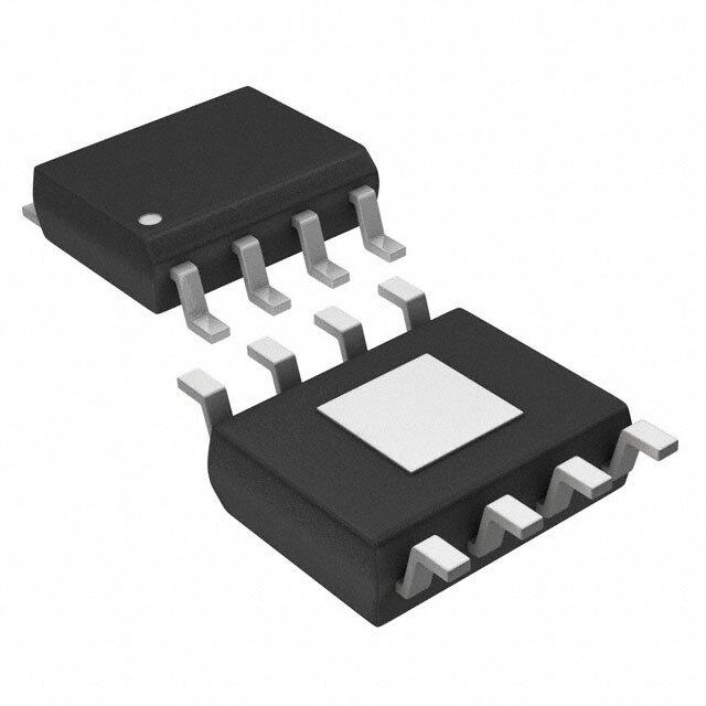
| 描述 | IC REG BUCK ADJ 3.5A TO263-5 |
| 产品分类 | |
| 品牌 | Sanken |
| 数据手册 | |
| 产品图片 | |
| 产品型号 | SI-8001FDE-TL |
| PWM类型 | 电流模式 |
| rohs | 无铅 / 符合限制有害物质指令(RoHS)规范要求 |
| 产品系列 | - |
| 供应商器件封装 | TO-263-5 |
| 其它名称 | SI-8001FDE-TLDKR |
| 包装 | Digi-Reel® |
| 同步整流器 | 无 |
| 安装类型 | 表面贴装 |
| 封装/外壳 | TO-263-6,D²Pak(5 引线+接片),TO-263BA |
| 工作温度 | -30°C ~ 85°C |
| 标准包装 | 1 |
| 电压-输入 | 4.5 V ~ 40 V |
| 电压-输出 | 0.8 V ~ 24 V |
| 电流-输出 | 3.5A |
| 类型 | 降压(降压) |
| 输出数 | 1 |
| 输出类型 | 可调式 |
| 频率-开关 | 300kHz |


- 商务部:美国ITC正式对集成电路等产品启动337调查
- 曝三星4nm工艺存在良率问题 高通将骁龙8 Gen1或转产台积电
- 太阳诱电将投资9.5亿元在常州建新厂生产MLCC 预计2023年完工
- 英特尔发布欧洲新工厂建设计划 深化IDM 2.0 战略
- 台积电先进制程称霸业界 有大客户加持明年业绩稳了
- 达到5530亿美元!SIA预计今年全球半导体销售额将创下新高
- 英特尔拟将自动驾驶子公司Mobileye上市 估值或超500亿美元
- 三星加码芯片和SET,合并消费电子和移动部门,撤换高东真等 CEO
- 三星电子宣布重大人事变动 还合并消费电子和移动部门
- 海关总署:前11个月进口集成电路产品价值2.52万亿元 增长14.8%


PDF Datasheet 数据手册内容提取
SI-8001FDE DC-to-DC Step-Down Converter Features and Benefits Description ▪ 3.5 A output current supplied in a small, surface mount The SI-8001FDE DC voltage regulator is a DC-to-DC buck power package convertor that attains an oscillation frequency of 300 kHz, ▪ High efficiency: 83% at V = 15 V, I = 2.0 A,V = 5 V and has an integrated miniaturized choke coil, allowing it to IN O O ▪ Requires only six external components (optional soft serve as a small, high efficiency power supply in a compact s start requires an additional capacitor) TO263 package. n ▪ Oscillation circuit built-in (frequency 300 kHz typical) The internal switching regulator fugnction provides high ▪ Constant-current mode overcurrent protection circuit and efficiency switching regulation withoiut any need for adjustment. overtemperature protection circuit built-in The device requires only six externsal support components. The ▪ Soft start function built-in (can be implemented as an e optional soft start function requires an additional capacitor. on/off function; output-off state at low level) D Optional on/off control can be performed using a transistor. ▪ Low current consumption during output-off state The SI-8001FDE includ es overcurrent and overtemperature w protection circuits. e Package: TO263-5 Applications include: N ▪ DVD recorder ▪ FPD TV r ▪ Telecommunications equipment o ▪ Office automation equipment, such as printers f ▪ On-board local power supply d▪ Output voltage regulator for second stage of SMPS e (switched mode power supply) d n e m Not to scale m o c Functional Block Diagram e R VIN 1 IN SW 2 L1 VOUT t oC1 PReg Overcurrent DDSPiiB-G56S C2 Protection N (Sanken) Latch and Reset Driver R1 5 SS On/Off Osc Soft Start C3 Comparator Overtemperature ADJ 4 Protection Error Amplifier R2 Reference Voltage GND 3 27469.056 SANKEN ELECTRIC CO., LTD. http://www.sanken-ele.co.jp/en/
SI-8001FDE DC-to-DC Step-Down Converter Selection Guide Output Voltage Efficiency, Input Voltage, Output Current, Part Number Adjustable Range Typ. Max. Max. Packing (V) (%) (V) (A) SI-8001FDE-TL 0.8 to 24 83 40 3.5 s800 pieces per reel n g i Absolute Maximum Ratings s e Characteristic Symbol Remarks Rating Units D DC Input Voltage V 43 V IN Mounted on 40 mm × 40 mm exposed copper area on 40 mm w Power Dissipation P × 40 mm glass-epoxy PCB; limited by internal overtemperature 3 W D protection. e Junction Temperature T Internal overtemperature protection cNircuit may enable when TJ ≥ –40 to 150 °C J 130°C. During product operation, recommended T ≤ 125°C. J Storage Temperature Tstg r –40 to 150 °C Mounted on 40 mm × 40 mom exposed copper area on 40 mm × Thermal Resistance (junction-to-case) R 3 °C/W JC 40 mm glass-epoxy PCfB. Mounted on 40 mm × 40 mm exposed copper area on 40 mm × Thermal Resistance (junction-to-ambient air) R d 33.3 °C/W JA 40 mm glass-epoxy PCB. e d n Recommended Operating Conditions* e m Characteristic Symbol Remarks Min. Max. Units DC Input Voltage Range Vm V (min) is the greater of 4.5 V or V +3 V. See 40 V IN IN O remarks DC Output Voltage Range o V 0.8 24 V O c V ≥ V + 3 V; to be used within the allowable package IN O DC Output Current Range e IO power dissipation characteristics (refer to Power Dissipation 0 3.5 A R chart). Operating Junction Temperature Range T –30 100 °C JOP t To be used within the allowable package power dissipation Operating Temperature Raonge TOP characteristics (refer to Power Dissipation chart). –30 85 °C N *Required for normal device functioning according to Electrical Characteristics table. All performance characteristics given are typical values for circuit or system baseline design only and are at the nominal operating voltage and an ambient temperature, T , of 25°C, unless oth er wise stated. A 2 27469.056 SANKEN ELECTRIC CO., LTD.
SI-8001FDE DC-to-DC Step-Down Converter ELECTRICAL CHARACTERISTICS1, valid at T = 25°C, V = 5 V (adjusted), R1 = 4.2 kΩ, R1 = 0.8 kΩ A O Characteristic Symbol Test Conditions1 Min. Typ. Max. Units Reference Voltage V V = 15 V, I = 0.2 A 0.784 0.800 0.816 V ADJ IN O Reference Voltage Temperature Coefficient ∆V /∆T V = 15 V, I = 0.2 A, T = 0 to 100 °C – ±0.1 – mV/°C ADJ IN O C Efficiency2 η V = 15 V, I = 2 A – 83 – % IN O Operating Frequency f V = 15 V, I = 2 A 270 300 330 kHz O IN O s Line Regulation V V = 10 to 30 V, I = 2 A – – 80 mV Line IN O n Load Regulation V V = 15 V, I = 0.2 to 3.5 A – – 50 mV Load IN O g Overcurrent Protection Threshold Current I V = 15 V 3.6 – – A S IN i SS Terminal On/Off Operation Threshold Voltage V s– – 0.5 V SSL e SS Terminal On/Off Operation Outflow Current I V = 0 V – 6 30 μA SSL SSL D Quiescent Current 1 I V = 15 V, I = 0 A – 6 – mA q IN O Quiescent Current 2 Iq(off) VIN = 15 V, VSS = 0 V w – 200 600 μA 1Using circuit shown in Typical Application Circuit diagram. e 2Efficiency is calculated as: η(%) = ([V × I ] × [V × I ]) × 100. O O IN IN N Pin-out Diagram Terminal List Table r Name Number o Function f IN 1 Supply voltage SW 2 Regulated supplyd output GND 3 Ground termeinal d ADJ 4 Terminal for resistor bridge feedback n The SS terminal is used to enable soft start and to control on/off operation of the IC output, VeO (see figure 2). If neither soft start nor on/off control is used, leave pin open. m To enable soft start, connect a capacitor between SS and ground. To control on/off operation, connect an NPN bipolar transistor, in a TTL open collector output configuration, m between the SS terminal and GND. Turn off is done by decreasing V below its rated SS 5 SSL level. o c When both soft start and VO on/off are used, a protection measure such as current limiting 1 2 3 4 5 is required because, if the capacitance of C3 large, the discharge current of C3 flows e across the transistor for on/off operation. Because a pull-up type resistor is provided inside R the IC, no external voltage can be applied. t o N SI-8000FDE SI-8000FDE SI-8000FDE SS SS SS 5 5 5 System C3 TTL System C3 TTL (a) (b) (c) V on/off Soft start V on/off and O O control only only soft start control Figure 2. Alternative configurations for SS pin. If neither soft start nor V on/off is required, the SS pin is left open. O 3 27469.056 SANKEN ELECTRIC CO., LTD.
SI-8001FDE DC-to-DC Step-Down Converter Performance Characteristics At T = 25°C, V = 5 V Adjusted, R1 = 4.2 kΩ, R2 = 0.8 kΩ A O 90 6.00 0 A 85 5.00 IO 8 V VIN 0.5 A s 15 V 80 4.00 1 An EOVfOuf=itcp 3iue.3tn CcVyu rvreernstus η (%)75 2300 V V LBOoeuwhtpa Vuvtoi oVltrao: glteage V (V)O3.00 i3.52g A A 70 versus 2.00 s 40 V Supply Voltage e 65 1.00 D 600 0.5 1.0 1.I5O (A)2.0 2.5 3.0 3.5 00 1w 2 3 VIN4 (V) 5 6 7 8 90 5.10 e 85 8 V 15 V VIN 55..N0086 VIN 5.04 80 Load Regulartion: 40 V EOVOfuf=itcp 5iue.0tn CcVyu rvreernstus η (%)75 2300 VV OvOeuurttsppfuuustt CVooulrtraegnet V (V) O554...009208 3105 VV 70 4.96 10 V d 40 V 4.94 65 e 8 V 4.92 d 4.90 60 0 0.5 1.0 1.I5O (A)2.0 2.5 3.n0 3.5 0 1 IO (2A) 3 100 e 10 m 95 15V 20 V VIN 8 m 90 EOVOfuf=itcp 1iue2tn. 0Cc yuV rvreernstus η (%)8850 ec30 Vo SQvSIOeSuu =rp is pe0puisn lsAyc o eVpnoet lnCtaugrerentI (mA) q46 R 40 V 2 75 o t 700 0.5 1.0 1.5IO (A)2.0 2.5 3.0 3.5 00 10 V2I0N (V) 30 40 N 400 6 5 Behavior at 300 8 V Overcurrent Turn-Off: Protection: 4 VIN Quiescent Current 15 V vIneprusut sV oltage I (μA)Q200 OvOeuurttsppuuustt CVoulrtraegnet V(V) O 3 30 V I = 0 A VO = 0 V 2 SS 40 V 100 1 0 0 0 0.5 1.0 1.5VIN (V2).0 2.5 3.0 3.5 0 1 2 IO (A)3 4 5 4 27469.056 SANKEN ELECTRIC CO., LTD.
SI-8001FDE DC-to-DC Step-Down Converter Thermal Performance Characteristics The application must be designed to ensure that the T(max) J Power Dissipation versus Ambient Temperature of the device is not exceeded during operation. To do so, it is T(max) = 125°C; Mounted on glass-epoxy PCB (40 mm × 40 mm), J with varying exposed copper areas necessary to determine values for maximum power dissipation, 3.5 P (max), and ambient temperature, T (max). D A Cu Area: 1600 mm2 The relationships of TJ, PD, TA, and case temperature, TC, are as RθJA = 33.3°C/W s shown in the following formulas: 3.0 n g T – T T – T Cu Area: 800 mm2 PD = JR C and PD = RJ A . 2.5 siRθJA = 37°C/W θJC θJA e P can be calculated from input values: D D Cu Area: 400 mm2 P =V ⋅I ⎜⎛100−1⎟⎞−V ⋅I ⎜⎛1− VO ⎟⎞ W) 2.0 w RθJA = 44°C/W D O O⎜⎝ (cid:72)x ⎟⎠ F O⎜⎝ VIN ⎟⎠ P (D e Cu Area: 100 mm2 where: 1.5 N RθJA = 53°C/W V is output voltage in V, O r 1.0 V is input supply voltage in V, IN o I is output current in A, f O d 0.5 η is IC efficiency in percent (varies with V and I ; refer to x IN O efficiency performance curves for value), and e d V is forward voltage for the input diode, Di. In these tests, the 0 F n –25 0 25 50 75 100 125 Sanken SPB-G56S was used, at 0.4 V. For application design, e TA (°C) obtain thermal data from the datasheet for the diode. m Device Thermal Resistance versus Exposed Copper Area on PCB PD is substantially affected by the heat conductance properties of Glass-epoxy PCB, 40 mm × 40 mm the application, in particular any exposed coppmer area on the PCB 55 where the device is mounted. The relationoships of PD, TA, and W) 50 copper area is represented in the Power Dissipation chart. C/ 45 c (°A 40 RθJA for a given copper area can be edetermined form the Device RθJ 35 Thermal Resistance chart. This cRan be substituted into the formula 30 above to determine the T (max) allowable in the application. J 0 200 400 600 800 1000 1200 1400 1600 1800 Generally, more than 10% tto 20% derating is required. Copper Area (mm2) o Because the heat dissipation capacity of the copper area depends N substantively on how it is used in the actual application, thermal 6 characteristics of the application must be confirmed by testing. OTP On T is determined by connecting a thermocouple to the device as 5 C shown here: Overtemperature 4 Protection: V) Output Voltage versus (O 3 Junction Temperature V Thermocouple mount V = 15 V, I = 10 mA at tab center IN O 2 1 And analyzing the results using the following formula: OTP Off T =P × R + T , 0 J D θJC C 0 20 40 60 80 100 120 140 160 180 for this device, R is 3 °C/W. TJ (°C) θJC 5 27469.056 SANKEN ELECTRIC CO., LTD.
SI-8001FDE DC-to-DC Step-Down Converter Component Selection Diode Di A Schottky-barrier diode must be used for Di. If other C2 or C3, because the extremely low ESR causes an abnormal diode types are used, such as fast recovery diodes, the IC may be oscillation. destroyed because of the reverse voltage applied by the recovery The device is stabilized, and for proper operation, C1 must be voltage or ON voltage. located close to the device (see layout diagram, below). C3 is s Choke Coil L1 If the winding resistance of the choke coil is too required only if the soft start function is usned. If not using soft- high, the efficiency may be reduced below rating. Because the start, leave the SS terminal open. A pullg-up resistor is provided overcurrent protection start current is approximately 4.2 A, atten- inside the IC. i tion must be paid to the heating of the choke coil by magnetic s Resistor Bridge R1 and R2 ceomprise the resistor bridge for the saturation due to overload or short-circuited load. output voltage, V , and are cDalculated as follows: O Capacitors C1, C2, and C3 Because for SMPS, large ripple R1=(VO−VADJ)=(VO−0 .8)(Ω) , and R2=VADJ = 0.8 =0.8(kΩ) currents flow across C1 and C2, capacitors with high frequency IADJ 1×w10−3 IADJ 1×10⁻³ and low impedance must be used. If the impedance of C2 is too I should always be set to 1 mA. Note that R2 should always be ADJ e high, the switching waveform may not be normal at low tempera- present to ensure stable operation, even if V , is set to 0.8 V (that N O tures. Do not use either OS or tantalum types of capacitors for is, even if there is no R1). V should be at least V + 8%. O IN r o f Typical Applicati on Diagram d L1 e VIN 1 2 VO Component Rating d IN SW C1 470 μF SI-8001FDE R1 n C2 680 μF SS GND ADJ 4 IADJm e CLD13i 0S4.7P1 B μμH-FG 5(F6oSr (sSoaftn skteanrt) function) C1 5 3 Di R2 C2 C3 m GND Soft Start Only GND o Recommended PCBc Layout Recommended Solder Pad Layout e R 11±0.2 t o N 9±0.2 6.8±0.1 9±0.1 3.7±0.05 4±0.1 1±0.05 All external components should be mounted as close as possible 1.7±0.1 to the SI-8001FDE. The ground of all components should be (mm) connected at one point near GND pin (pin 3). 6 27469.056 SANKEN ELECTRIC CO., LTD.
SI-8001FDE DC-to-DC Step-Down Converter PACKAGE OUTLINE DRAWING 9.90 ±0.20 0 2 4.50 ±0.20 (8.00) 0. 15º 3XR0.30 1.30+–00..0150 (0.75) n(4.4s0) (0.40) 2.20 ± g Ø1.5 ±0.20 + + Branding XXXXXXXXXXXXXXXXXXXXXXXX (4.60) 20 3XR0.303º esi(R0.45) 6.80) 0. 0 D ( XXXXXXXX 9.20 ± 5.30 ±0.3 0 ±0.10 0.10 ±0.15 w 1 0 2. e 3º 3º 2.4N0 ±0.20 0 2 0. ± 0 r 0.88 ±0.10 4.9 75) (R0.30)(0.o50) 0. ( f 0 0.80 ±0.10 6º 0.3 d 0º 4 ± 4×P1.70 ±0.25 e 2.5 d 3º 2XR0.30 n e m m 1 2 3 4 5 10.00 ±0.02 Branding codes (exact appearance at manufacturer discretion): o c Dimensions do not include moeld protrusion 1st line: SK Heastsink side flash: 0.8 mm maximum 2nd line, lot: YMW X R Where: Y is the last digit of the year of manufacture M is the month (1 to 9, O, N, D) Dimensions in millimteters W is the week of the month (1 to 5) o X is the device subtype suffix number 3rd line, type: 8001FDE N RoHS directive compliant Device pins lead (Pb) free 7 27469.056 SANKEN ELECTRIC CO., LTD.
SI-8001FDE DC-to-DC Step-Down Converter s n g i s e Cautions for Use solder bath must be groundeDd in other to prevent leak voltages • Operation of the product in parallel to increase current is not generated by them from being applied to the products. permitted. • The products should awlways be stored and transported in our • Although the product has an internal overtemperature protection shipping containers or conductive containers, or be wrapped in circuit, that is intended only to protect the product from temporary e excess heating due to overloads. Long-term reliability cannot aluminum foil. N be guaranteed when the product is operated under continuous Soldering overload conditions. Because reliability can be affected adversely by improper storage • Whenr manually soldering the products, please be sure to environments and handling methods, please observe the following minoimize the working time, within the following limits: cautions. f Cautions for Storage Soldering Iron Temperature Time • Ensure that storage conditions comply with the standard d (°C) (s) temperature (5°C to 35°C) and the standard relative humidity e 3 (around 40 to 75%); avoid storage locations that experience d 380±10 (once only) extreme changes in temperature or humidity. • Avoid locations where dust or harmful gases are present and n avoid direct sunlight. • Reflow soldering can be performed a maximum of twice, using e • Reinspect for rust on leads and solderability of products that have the following recommended profile: m been stored for a long time. Cautions for Testing and Handling When tests are carried out during inspection testming and other 250 250°C Maximum standard test periods, protect the products from power surges 230 from the testing device, shorts between adjoacent products, and C) shorts to the heatsink. c e (° Electrostatic Discharge e atur • When handling the products, opeRrator must be grounded. per180 Grounded wrist straps worn should have at least 1 MΩ of m e resistance to ground to prevent shock hazard. T 30±10s • Workbenches where the ptroducts are handled should be 150 grounded and be providoed with conductive table and floor mats. • When using measurNing equipment such as a curve tracer, the 90±30s equipment should be grounded. Time • When soldering the products, the head of soldering irons or the 8 27469.056 SANKEN ELECTRIC CO., LTD.
SI-8001FDE DC-to-DC Step-Down Converter s n g i s e D • The contents in this document are subject to changes, for improvement and other purposes, without notice. Make sure that this is the w latest revision of the document before use. e • Application and operation examples described in this document are quoted for the sole purpose of reference for the use of the prod- N ucts herein and Sanken can assume no responsibility for any infringement of industrial property rights, intellectual property rights or any other rights of Sanken or any third party which may result from its use. r • Although Sanken undertakes to enhance the quality and reliability of its poroducts, the occurrence of failure and defect of semicon- ductor products at a certain rate is inevitable. Users of Sanken products are requested to take, at their own risk, preventative measures f including safety design of the equipment or systems against any poss ible injury, death, fires or damages to the society due to device d failure or malfunction. e • Sanken products listed in this document are designed and intended for the use as components in general purpose electronic equip- d ment or apparatus (home appliances, office equipment, telecommunication equipment, measuring equipment, etc.). n When considering the use of Sanken products in the applications where higher reliability is required (transportation equipment and e its control systems, traffic signal control systems or equipment, fire/crime alarm systems, various safety devices, etc.), and whenever m long life expectancy is required even in general purpose electronic equipment or apparatus, please contact your nearest Sanken sales representative to discuss, prior to the use of thme products herein. The use of Sanken products without the written consent of Sanken in the applications where extremely high reliability is required o (aerospace equipment, nuclear power control systems, life support systems, etc.) is strictly prohibited. c • In the case that you use Sanken products or design your products by using Sanken products, the reliability largely depends on the e degree of derating to be made tRo the rated values. Derating may be interpreted as a case that an operation range is set by derating the load from each rated value or surge voltage or noise is considered for derating in order to assure or improve the reliability. In general, derating factors include electric stresses such as electric voltage, electric current, electric power etc., environmental stresses such t as ambient temperatureo, humidity etc. and thermal stress caused due to self-heating of semiconductor products. For these stresses, instantaneous valueNs, maximum values and minimum values must be taken into consideration. In addition, it should be noted that since power devices or IC's including power devices have large self-heating value, the degree of derating of junction temperature affects the reliability significantly. • When using the products specified herein by either (i) combining other products or materials therewith or (ii) physically, chemically or otherwise processing or treating the products, please duly consider all possible risks that may result from all such uses in advance and proceed therewith at your own responsibility. • Anti radioactive ray design is not considered for the products listed herein. • Sanken assumes no responsibility for any troubles, such as dropping products caused during transportation out of Sanken's distribu- tion network. • The contents in this document must not be transcribed or copied without Sanken's written consent. 9 27469.056 SANKEN ELECTRIC CO., LTD.