 Datasheet下载
- 型号: SESD0402P1BN-0450-090
- 制造商: CORCOM/TYCO ELECTRONICS
- 库位|库存: xxxx|xxxx
- 要求:
| 数量阶梯 | 香港交货 | 国内含税 |
| +xxxx | $xxxx | ¥xxxx |
查看当月历史价格
查看今年历史价格
SESD0402P1BN-0450-090产品简介:
ICGOO电子元器件商城为您提供SESD0402P1BN-0450-090由CORCOM/TYCO ELECTRONICS设计生产,在icgoo商城现货销售,并且可以通过原厂、代理商等渠道进行代购。 SESD0402P1BN-0450-090价格参考。CORCOM/TYCO ELECTRONICSSESD0402P1BN-0450-090封装/规格:TVS - 二极管, 。您可以下载SESD0402P1BN-0450-090参考资料、Datasheet数据手册功能说明书,资料中有SESD0402P1BN-0450-090 详细功能的应用电路图电压和使用方法及教程。
Littelfuse Inc. 生产的型号为 SESD0402P1BN-0450-090 的 TVS(瞬态电压抑制)二极管,主要用于保护电子设备免受瞬态电压尖峰的影响。这种二极管具有快速响应时间和低电容特性,适用于高速数据线和信号线的保护。以下是该型号的具体应用场景:

 1. 消费电子产品
   在智能手机、平板电脑、笔记本电脑等消费电子产品中,SESD0402P1BN-0450-090 可以用于保护 USB 接口、HDMI 接口、耳机插孔等外部连接器,防止静电放电(ESD)和其他瞬态电压对内部电路造成损害。由于其小尺寸(0402 封装),非常适合在紧凑的设计中使用。

 2. 通信设备
   在路由器、调制解调器、交换机等网络设备中,该 TVS 二极管可以用于保护以太网端口、Wi-Fi 模块、蓝牙模块等接口,防止雷击感应电压或电源波动引起的瞬态电压损坏设备。它还可以用于保护天线接口,防止射频信号中的瞬态干扰。

 3. 工业控制
   在工业自动化系统中,如可编程逻辑控制器(PLC)、传感器、执行器等设备中,SESD0402P1BN-0450-090 可以用于保护数字输入/输出接口、通信总线(如 RS-485、CAN 总线)等,确保在恶劣环境下设备的稳定性和可靠性。

 4. 汽车电子
   在汽车电子系统中,该 TVS 二极管可以用于保护车载信息娱乐系统、导航系统、倒车雷达等设备的接口,防止车辆启动时的电压波动或外界电磁干扰对系统的影响。此外,它还可以用于保护车内网络通信线路,确保数据传输的稳定性。

 5. 医疗设备
   在便携式医疗设备(如血糖仪、心率监测仪)和大型医疗设备(如超声波设备、CT 扫描仪)中,SESD0402P1BN-0450-090 可以用于保护患者接口、传感器接口以及通信接口,确保设备在使用过程中不会因为瞬态电压而出现故障,保障患者的安全。

总之,SESD0402P1BN-0450-090 是一种高性能的 TVS 二极管,适用于各种需要高可靠性和抗干扰能力的应用场景,尤其是在对瞬态电压敏感的电子设备中表现尤为突出。
| 参数 | 数值 |
| 产品目录 | |
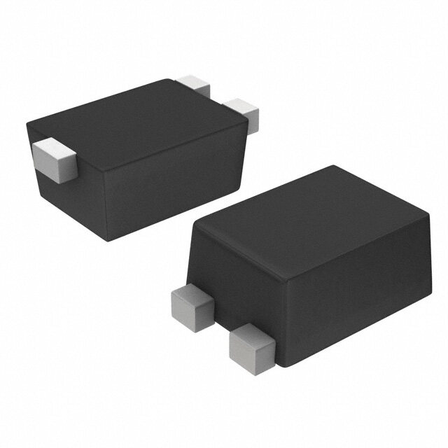
| 描述 | TVS DIODE 6VWM 12VC 0402ESD 抑制器 0402 PKG 9V 4.5pF SESD PROTECTOR |
| 产品分类 | |
| 品牌 | TE Connectivity / Raychem |
| 产品手册 | |
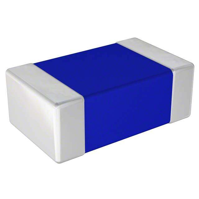
| 产品图片 |
|
| rohs | 符合RoHS无铅 / 符合限制有害物质指令(RoHS)规范要求 |
| 产品系列 | TE Connectivity / Raychem SESD0402P1BN-0450-090Raychem |
| mouser_ship_limit | 该产品可能需要其他文件才能进口到中国。 |
| 数据手册 | |
| 产品型号 | SESD0402P1BN-0450-090 |
| 不同频率时的电容 | 4.5pF @ 1MHz |
| 产品种类 | ESD 抑制器 |
| 供应商器件封装 | 0402 |
| 其它名称 | SESD0402P1BN-0450-090CT |
| 击穿电压 | 11 V |
| 功率-峰值脉冲 | - |
| 包装 | 剪切带 (CT) |
| 单向通道 | - |
| 双向通道 | 1 |
| 商标 | TE Connectivity / Raychem |
| 安装类型 | 表面贴装 |
| 封装 | Reel |
| 封装/外壳 | 0402(1005 公制) |
| 封装/箱体 | 0402 (1005 metric) |
| 工作温度 | -40°C ~ 125°C |
| 工作温度范围 | - 40 C to + 125 C |
| 工厂包装数量 | 10000 |
| 应用 | 通用 |
| 标准包装 | 1 |
| 电压-击穿(最小值) | 9V |
| 电压-反向关态(典型值) | 6V (最小值) |
| 电压-箝位(最大值)@Ipp | 12V |
| 电容 | 4.5 pF |
| 电流-峰值脉冲(10/1000µs) | 2A (8/20µs) |
| 电源线路保护 | 无 |
| 端接类型 | SMD/SMT |
| 类型 | 齐纳 |
| 系列 | SESD |
| 通道 | 1 Channel |
| 零件号别名 | RF2012-000 |


- 商务部:美国ITC正式对集成电路等产品启动337调查
- 曝三星4nm工艺存在良率问题 高通将骁龙8 Gen1或转产台积电
- 太阳诱电将投资9.5亿元在常州建新厂生产MLCC 预计2023年完工
- 英特尔发布欧洲新工厂建设计划 深化IDM 2.0 战略
- 台积电先进制程称霸业界 有大客户加持明年业绩稳了
- 达到5530亿美元!SIA预计今年全球半导体销售额将创下新高
- 英特尔拟将自动驾驶子公司Mobileye上市 估值或超500亿美元
- 三星加码芯片和SET,合并消费电子和移动部门,撤换高东真等 CEO
- 三星电子宣布重大人事变动 还合并消费电子和移动部门
- 海关总署:前11个月进口集成电路产品价值2.52万亿元 增长14.8%


PDF Datasheet 数据手册内容提取
ChipSESD PRODUCT: SESD0402P1BN-0450-090 Silicon ESD Protector DOCUMENT: SCD27764 Overvoltage Protection Device REV LETTER: B Circuit Protection Products REV DATE: JULY 26, 2016 PAGE NO.: 1 OF 5 Specification Status: Released BENEFITS Silicon ESD device in an EIA-0402 size rectangular passive component SMT package Standard PCB assembly and rework processes Bi-directional operation allows placement on PCB without orientation constraint Appropriate for ESD protection in space-constrained portable electronics and mobile handsets Suitable for +5V operating voltage applications Helps protect electronic circuits against damage from Electrostatic Discharge (ESD) events Assist equipment to pass IEC61000-4-2, level 4 testing RoHS compliant and Halogen Free PART NUMBERING FEATURES SESD 0402 P1BN- 0450- 090 Input capacitance – 4.5pF (typ) Series Breakdown Voltage Low leakage current – 1.0µA (max) EIA Size 9.0V (min) Low working reverse voltage – 6.0V (max) Input Capacitance ESD maximum rating per IEC61000-4-2 standard Package Type 4.5 pF (typ) o ± 10kV contact discharge(1) P - Packaged SMD .. o ± 16kV air discharge Capable of withstanding numerous ESD strikes 1 - one channel N - No Common pin B - Bidirectional Small package size: 1.10mm x 0.50mm (typ) MATERIALS Low package height: 0.50mm (typ) INFORMATION RoHS Compliant ELV Compliant Halogen Free * APPLICATIONS HF Cellular phones and portable electronics Digital cameras and camcorders * Halogen Free refers to: Br≤900ppm, Cl≤900ppm, Br+Cl≤1500ppm USB 2.0 and computer I/O ports Terminal finish: 100% Matte Tin (Sn) Notebooks, set top boxes, motherboards Applications requiring high ESD performance Device Characteristics @ T = 25oC Min Typ Max Unit Input Capacitance @ Vr = 0V, f = 1MHz -- 4.5 5.5 pF Working Reverse Voltage (peak) - VRWM -- -- 6.0 V Breakdown Voltage – Vbr @ It = 1mA(2) 9.0 11.0 -- V Leakage current @ VRWM = 6.0V -- -- 1.0 µA Clamping Voltage @ Ipp=2A, tp=(8/20µs) -- ±10.0 ±12.0 V ESD contact discharge per IEC61000-4-2 standard (1) -- -- ±10 kV ESD air discharge per IEC61000-4-2 standard -- -- ±16 kV Operating (Tjunction) and Storage Temperature Range -40 to +125 ˚C (1) 10kV @ 50 ± pulses under IEC61000-4-2; 8kV @ 1,000 pulses under IEC61000-4-2 (2) Vbr is measured at test current It © 2016 Littelfuse,Inc. littelfuse.com Specifications are subject to change without notice. Revised July 26, 2016
ChipSESD PRODUCT: SESD0402P1BN-0450-090 Silicon ESD Protector DOCUMENT: SCD27764 Overvoltage Protection Device REV LETTER: B Circuit Protection Products REV DATE: JULY 26, 2016 PAGE NO.: 2 OF 5 DEVICE DIMENSIONS AAAA BB CC DD DD Drawings Not To Scale Typical A B C D mm 1.10 ± 0.1 0.50 ± 0.1 0.50 ± 0.1 0.25 ± 0.15 mils* 43.31 ± 4.0 19.69 ± 4.0 19.69 ± 4.0 9.84 ± 6.0 * Round off approximation RECOMMENDED LANDING PATTERN: PPCC BBooaarrdd WW PPaadd PPaadd LL SS LL Typical L S W mm 0.61 ± 0.05 0.52 ± 0.05 0.50 ± 0.05 mils* 24.0 ± 2.0 21.0 ± 2.0 20.0 ± 2.0 * Round off approximation Recommended solder thickness: 150 to 200 um Recommended rework procedure: o Soldering iron tip temperature should be less than 350oC o Apply iron tip to solder for less than 5 seconds o Do not apply solder iron tip to the body of this product directly © 2016 Littelfuse,Inc. littelfuse.com Specifications are subject to change without notice. Revised July 26, 2016
ChipSESD PRODUCT: SESD0402P1BN-0450-090 Silicon ESD Protector DOCUMENT: SCD27764 Overvoltage Protection Device REV LETTER: B Circuit Protection Products REV DATE: JULY 26, 2016 PAGE NO.: 3 OF 5 PACKAGING Packaging Tape & Reel Standard Box SESD0402P1BN-0450-090 10,000 50,000 REEL DIMENSIONS LLaabbeell Dimension A B C D E F G (mm) 178.0 ± 2.0 2.0 ± 0.5 13.0 ± 0.5 21.0 ± 0.8 62.0 ± 1.5 9.0 ± 0.5 13.0 ± 1.0 CARRIER TAPE DIMENSIONS Dimension A B D E F W (mm) 0.58 ± 0.03 1.20 ± 0.03 1.55 ± 0.05 1.75 ± 0.05 3.5 ± 0.05 8.0 ± 0.1 Dimension P P P T 0 1 2 (mm) 4.0 ± 0.1 2.0 ± 0.05 2.0 ± 0.05 0.60 ± 0.03 © 2016 Littelfuse,Inc. littelfuse.com Specifications are subject to change without notice. Revised July 26, 2016
ChipSESD PRODUCT: SESD0402P1BN-0450-090 Silicon ESD Protector DOCUMENT: SCD27764 Overvoltage Protection Device REV LETTER: B Circuit Protection Products REV DATE: JULY 26, 2016 PAGE NO.: 4 OF 5 FIGURE 1: TYPICAL IV CURVE SESD0402 Typical IV Chart @ 1mA 1.00E-03 8.00E-04 6.00E-04 4.00E-04 A ) 2.00E-04 nt ( 0.00E+00 e urr -12 -10 -8 -6 -4 -2 0 2 4 6 8 10 12 C -2.00E-04 -4.00E-04 -6.00E-04 -8.00E-04 -1.00E-03 Voltage ( V ) FIGURE 2: ESD CLAMPING VOLTAGE – 8kV Contact SESD0402 ESD 8kV contact per IEC61000-4-2 Level 4 350 300 250 V ) e ( 200 g olta 150 V 100 50 0 0 20 40 60 80 100 Time (nSec) © 2016 Littelfuse,Inc. littelfuse.com Specifications are subject to change without notice. Revised July 26, 2016
ChipSESD PRODUCT: SESD0402P1BN-0450-090 Silicon ESD Protector DOCUMENT: SCD27764 Overvoltage Protection Device REV LETTER: B Circuit Protection Products REV DATE: JULY 26, 2016 PAGE NO.: 5 OF 5 FIGURE 3: ESD CLAMPING VOLTAGE – 8x20µs, 2A Surge SESD0402 Typical Clamping Performance under a 8x20µs, 2A Surge 14 12 10 V) 8 e ( g a olt 6 V 4 2 0 0.0E+00 1.0E-04 2.0E-04 3.0E-04 4.0E-04 5.0E-04 6.0E-04 7.0E-04 8.0E-04 9.0E-04 1.0E-03 Time (S) Littelfuse products are not designed for, and shall not be used for, any purpose (including, without limitation, automotive, military, aerospace, medical, life-saving, life-sustaining or nuclear facility applications, devices intended for surgical implant into the body, or any other application in which the failure or lack of desired operation of the product may result in personal injury, death, or property damage) other than those expressly set forth in applicable Littelfuse product documentation. Warranties granted by Littelfuse shall be deemed void for products used for any purpose not expressly set forth in applicable Littelfuse documentation. Littelfuse shall not be liable for any claims or damages arising out of products used in applications not expressly intended by Littelfuse as set forth in applicable Littelfuse documentation. The sale and use of Littelfuse products is subject to Littelfuse Terms and Conditions of Sale, unless otherwise agreed by Littelfuse. © 2016 Littelfuse,Inc. littelfuse.com Specifications are subject to change without notice. Revised July 26, 2016