ICGOO在线商城 > 电路保护 > TVS - 混合技术 > SEP0080Q38CB

 Datasheet下载
- 型号: SEP0080Q38CB
- 制造商: Littelfuse
- 库位|库存: xxxx|xxxx
- 要求:
| 数量阶梯 | 香港交货 | 国内含税 |
| +xxxx | $xxxx | ¥xxxx |
查看当月历史价格
查看今年历史价格
SEP0080Q38CB产品简介:
ICGOO电子元器件商城为您提供SEP0080Q38CB由Littelfuse设计生产,在icgoo商城现货销售,并且可以通过原厂、代理商等渠道进行代购。 SEP0080Q38CB价格参考¥20.00-¥25.00。LittelfuseSEP0080Q38CB封装/规格:TVS - 混合技术, 。您可以下载SEP0080Q38CB参考资料、Datasheet数据手册功能说明书,资料中有SEP0080Q38CB 详细功能的应用电路图电压和使用方法及教程。
Littelfuse Inc.的SEP0080Q38CB是一款TVS(瞬态电压抑制器)混合技术器件,主要用于保护敏感电子设备免受瞬态电压尖峰的影响。以下是其主要应用场景:

 1. 汽车电子系统
   在现代汽车中,电子控制系统越来越复杂,包括发动机控制单元(ECU)、车身控制模块(BCM)、车载娱乐系统等。这些系统中的传感器、通信接口(如CAN总线、LIN总线)和电源线容易受到瞬态电压的干扰。SEP0080Q38CB可以有效保护这些电路,防止由于电感负载切换、电池短路或雷击引起的电压尖峰对系统的损害。

 2. 工业自动化设备
   工业环境中,电机驱动器、可编程逻辑控制器(PLC)、传感器和执行器等设备经常暴露在恶劣的电气环境中。瞬态电压可能由开关操作、感应负载或电网波动引起。SEP0080Q38CB能够为这些设备提供可靠的过电压保护,确保工业自动化系统的稳定运行。

 3. 通信设备
   通信基础设施中的设备,如基站、路由器、交换机和无线接入点,通常需要在户外或半户外环境中工作。这些设备容易受到雷击、静电放电(ESD)和其他瞬态事件的影响。SEP0080Q38CB可以保护通信端口、天线接口和电源输入端,防止瞬态电压损坏内部电路,确保通信链路的可靠性。

 4. 消费电子产品
   消费电子产品如智能手机、平板电脑、笔记本电脑和智能家居设备也面临瞬态电压的威胁,尤其是在充电过程中或通过USB接口进行数据传输时。SEP0080Q38CB可以用于保护这些设备的电源线和信号线,防止因插拔操作或外部电源波动导致的损坏。

 5. 医疗设备
   医疗设备如心电图机、超声波设备和监护仪等对电磁兼容性和安全性要求极高。瞬态电压可能会导致设备误操作或数据丢失,影响诊断结果甚至患者安全。SEP0080Q38CB能够为这些设备的关键电路提供保护,确保其在各种环境下的可靠性和安全性。

总之,SEP0080Q38CB凭借其快速响应时间和低箝位电压特性,广泛应用于需要高可靠性和高性能保护的各种电子设备中,特别是在那些容易受到瞬态电压影响的环境中。
| 参数 | 数值 |
| 产品目录 | |
| 描述 | SIDACTOR ETHERNET POE 8V 100A硅对称二端开关元件 SEP Ethernet 100A Biasd Protec. Device |
| 产品分类 | TVS - 其它复合分离式半导体 |
| 品牌 | Littelfuse |
| 产品手册 | |
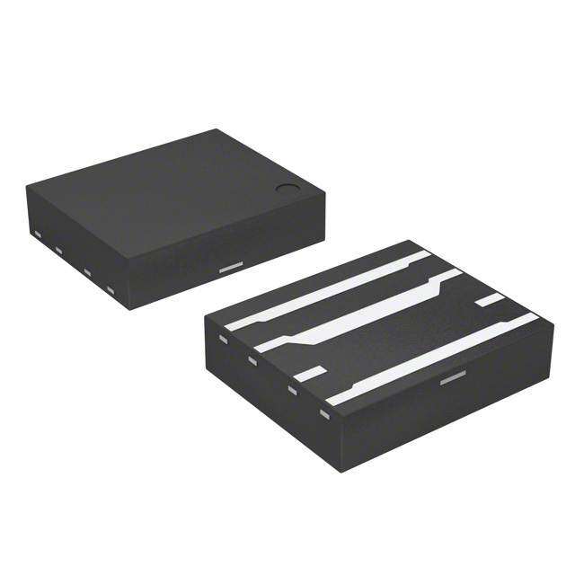
| 产品图片 |
|
| rohs | 符合RoHS不受无铅要求限制 / 符合限制有害物质指令(RoHS)规范要求 |
| 产品系列 | 晶体闸流管,硅对称二端开关元件,Littelfuse SEP0080Q38CBSIDACtor® |
| 数据手册 | |
| 产品型号 | SEP0080Q38CB |
| 不重复通态电流 | 30 A |
| 产品培训模块 | http://www.digikey.cn/PTM/IndividualPTM.page?site=cn&lang=zhs&ptm=23919http://www.digikey.cn/PTM/IndividualPTM.page?site=cn&lang=zhs&ptm=24669 |
| 产品目录页面 | |
| 产品种类 | 硅对称二端开关元件 |
| 供应商器件封装 | 8-QFN(5x6) |
| 保持电流Ih最大值 | 80 mA |
| 关闭状态漏泄电流(在VDRMIDRM下) | 5 uA |
| 关闭状态电容CO | 15 pF to 25 pF |
| 其它名称 | SEP0080Q38CBDKR |
| 功率(W) | - |
| 包装 | Digi-Reel® |
| 商标 | Littelfuse |
| 安装风格 | SMD/SMT |
| 封装 | Reel |
| 封装/外壳 | 8-LQFN |
| 封装/箱体 | QFN-8 |
| 工作结温 | - 40 C to + 150 C |
| 工厂包装数量 | 4000 |
| 应用 | 以太网 |
| 开启状态电压 | 8 V |
| 技术 | 混合技术 |
| 最大工作温度 | + 85 C |
| 最大转折电流IBO | 800 mA |
| 最小工作温度 | - 40 C |
| 标准包装 | 1 |
| 电压-工作 | 6V |
| 电压-箝位 | 8V |
| 电流额定值 | 2.2 A |
| 电路数 | 2 |
| 系列 | SEPXXXXQ38CB |
| 转折电流VBO | 25 V |
| 额定重复关闭状态电压VDRM | 6 V |


- 商务部:美国ITC正式对集成电路等产品启动337调查
- 曝三星4nm工艺存在良率问题 高通将骁龙8 Gen1或转产台积电
- 太阳诱电将投资9.5亿元在常州建新厂生产MLCC 预计2023年完工
- 英特尔发布欧洲新工厂建设计划 深化IDM 2.0 战略
- 台积电先进制程称霸业界 有大客户加持明年业绩稳了
- 达到5530亿美元!SIA预计今年全球半导体销售额将创下新高
- 英特尔拟将自动驾驶子公司Mobileye上市 估值或超500亿美元
- 三星加码芯片和SET,合并消费电子和移动部门,撤换高东真等 CEO
- 三星电子宣布重大人事变动 还合并消费电子和移动部门
- 海关总署:前11个月进口集成电路产品价值2.52万亿元 增长14.8%


PDF Datasheet 数据手册内容提取
SIDACtor® Protection Thyristors Broadband OptimizedTM Protection SEP Biased Series - 5x6 QFN RoHS Pb e3 Description The new SEP (SIDACtor Thyristor Ethernet/PoE Protector) series has a surge rating compatible with GR1089 inter-building and ITU K.20/21 Enhanced protection requirements. Targeted for high-speed applications such as 10BaseT, 100BaseT, and 1000BaseT, the SEP series maintains signal quality while providing robust protection for Ethernet and PoE applications. This latest silicon design innovation results in a capacitive loading characteristic that is constant with respect to the voltage across the component. This reduces distortion caused by typical solid-state protection solutions. Offered in a surface-mount, QFN package, the SEP provides small package size without Agency Approvals sacrificing power and surge handling capabilities. Agency Agency File Number E133083 Features & Benefits • C ompatible with • F ails short circuit when Pinout Designation 1000Base-T surged in excess of ratings Line in 1 8 Line out • B alanced overvoltage • R oHS Compliant and - Bias 2 7 + Bias protection Halogen-Free Ground 3 6 Ground • L ow distortion • P b-free E3 means 2nd level Line in 4 5 Line out interconnect is Pb-free and • L ow insertion loss the terminal finish material Schematic Symbol • L ow profile is tin(Sn) (IPC/JEDEC J-STD-609A.01) • SO-8 footprint compatible Line In (1) (8) Line Out Applicable Global Standards -Bias (2) (7) +Bias • TIA-968-A • GR 1089 Intra-building Ground (3) (6) Ground • TIA-968-B • YD/T 1082 Line In (4) (5) Line Out • I TU K.20/21 Enhanced • YD/T 993 8002 tcO snevaH pillihP Level • YD/T 950 Additional Information • I TU K.20/21 Basic Level • Class 4/5 compliance of • I EC 61000-4-5 2nd edition IEC 61000--4-5 • G R 1089 Inter-building Datasheet Resources Samples Electrical Characteristics V @ V@I= DRM V @100V/µs I I I@V T T Part Number Marking I =5µA S H S T T 2.2Amps Capacitance DRM V min V max mA min mA max A max V max SEP0080Q38CB SEP-8C 6 25 50 800 2.2 8 SEP0640Q38CB SEP06C 58 77 150 800 2.2 8 SEP0720Q38CB SEP07C 65 88 150 800 2.2 8 SEP0900Q38CB SEP09C 75 98 150 800 2.2 8 See Capacitance vs. SEP0080Q38BB SEP-8B 6 25 50 800 2.2 8 Bias Voltage Graph SEP0640Q38BB SEP06B 58 77 150 800 2.2 8 SEP0720Q38BB SEP07B 65 88 150 800 2.2 8 SEP0900Q38BB SEP09B 75 98 150 800 2.2 8 Notes: - Absolute maximum ratings measured at T= 25ºC (unless otherwise noted). A - Components are bidirectional (unless otherwise noted). © 2018 Littelfuse, Inc. Specifications are subject to change without notice. Revised: 08/29/18
SIDACtor® Protection Thyristors Broadband OptimizedTM Protection 50/60 Hz Ratings Parameter Name Test Conditions Value Units 0.5s 6.5 1s 4.6 I Maximum non-repetitive 2s 3.4 TSM A on-state current, 50/60 Hz 5s 2.3 30s 1.3 900s 0.73 Surge Ratings I I PP TSM Series 2x10µs 1.2/50µs-8/20µs 10/700-5/310µs 10x1000µs 600V 1 cycle RMS A min A min A min A min A RMS B 250 250 100 80 30 C 500 430 200 100 30 Notes: - Peak pulse current rating (I ) is repetitive and guaranteed for the life of the product as long as it returns to 25C° between surges - I ratings applicable over tePPmperature range of -40ºC to +85ºC PP - The components must initially be in thermal equilibrium with -40°C < T < +150°C J Thermal Considerations Package Symbol Parameter Value Unit T Junction Temperature -40 to +150 °C J T Storage Temperature Range -40 to +150 °C STG R Thermal Resistance: Junction to Ambient 100 °C/W 5x6 QFN 0JA V-I Characteristics Capacitance vs. Bias Voltage* +I 40 35 IT 30 Bi0aVs Voltage3.3V IS F) 5V 12V IH ce (p 25 2540VV 30V -V IDRM +V acitan 20 ap 15 VT VDRM C 10 VS 5 0 0.1 110 100 Line Voltage (V) -I * Bias voltage must be lower than V DRM © 2018 Littelfuse, Inc. Specifications are subject to change without notice. Revised: 08/29/18
SIDACtor® Protection Thyristors Broadband OptimizedTM Protection Normalized V Change vs. Junction Temperature Normalized DC Holding Current vs. Case Temperature S 2.0 14 e – % 1102 5ºC) 11..86 g 2 VChan S 468 25 °C IHI(T= H C 11..42 25°C of 2 of 1.0 ercent -40 Ratio 00..86 P -6 0.4 -8 -40 -20 0 20 40 60 80 100 120 140 160 -40 -20 0 20 40 60 80100120140 160 Case Temperature (T) - ºC Junction Temperature (T ) – °C C J Soldering Parameters Pb-Free assembly Reflow Condition (see Fig. 1) Figure 1 t P - Temperature Min (T ) +150°C T s(min) P Pre Heat - Temperature Max (Ts(max)) +200°C Ramp-up CriTtiLc atol ZToPne - Time (Min to Max) (t) 60-180 secs. s T Atov pereaagke) ramp up rate (Liquidus Temp (TL) 3°C/sec. Max. eruTS(maxL) tL t TS(max) to TL - Ramp-up Rate 3°C/sec. Max. are Ramp-down Reflow - Temperature (TL) (Liquidus) +217°C pmTS(min) Preheat - Temperature (tL) 60-150 secs. eT tS Peak Temp (T) +260(+0/-5)°C P 25 Time within 5°C of actual Peak Temp (tp) 30 secs. Max. time (tto 2 p5eºCak t ote pmepake)rature Time Ramp-down Rate 6°C/sec. Max. Time 25°C to Peak Temp (T) 8 min. Max. P Do not exceed +260°C Environmental Specifications Physical Specifications High Temp Voltage 80% Rated VDRM (VAC Peak ) +125°C or +150°C, 504 or 1008 hrs. MIL-STD-750 (Method 1040) Blocking JEDEC, JESD22-A-101 Lead Material Copper Alloy -65°C to +150°C, 15 min. dwell, 10 up to 100 Temp Cycling cycles. MIL-STD-750 (Method 1051) EIA/JEDEC, JESD22-A104 Terminal Finish 100% Matte-Tin Plated Biased Temp & 52 V (+85°C) 85%RH, 504 up to 1008 hrs. EIA/ DC Humidity JEDEC, JESD22-A-101 UL Recognized compound meeting Body Material flammability rating V-0 High Temp Storage +150°C 1008 hrs. MIL-STD-750 (Method 1031) JEDEC, JESD22-A-101 Low Temp Storage -65°C, 1008 hrs. 0°C to +100°C, 5 min. dwell, 10 sec. transfer, Thermal Shock 10 cycles. MIL-STD-750 (Method 1056) JEDEC, JESD22-A-106 Resistance to Solder +260°C, 30 secs. MIL-STD-750 (Method 2031) Heat Moisture Sensitivity 85%RH, +85°C, 168 hrs., 3 reflow cycles Level (+260°C Peak). JEDEC-J-STD-020, Level 1 © 2018 Littelfuse, Inc. Specifications are subject to change without notice. Revised: 08/29/18
SIDACtor® Protection Thyristors Broadband OptimizedTM Protection Dimensions — 5x6 QFN A Inches Millimeters Dimension 5 6 7 8 Min Max Min Max A 0.187 0.207 4.745 5.253 B 0.226 0.246 5.745 6.253 H K L B I D C 0.054 0.064 1.374 1.628 J D 0.165 0.171 4.199 4.351 E 4 3 2 I E 0.027 0.033 0.686 0.838 G F PIN 1 INDICATOR F 0.011 0.017 0.279 0.432 PIN 1 & 8: LINE IN / LINE OUT PIN 2: BIAS (-) G 0.047 0.053 1.194 1.346 PIN 3 & 6: GROUND CONNECTIONS C PIN 4 & 5: LINE IN / LINE OUT PIN 7: BIAS (+) H 0.032 0.038 0.800 0.953 F (REF) G (REF) I 0.027 0.033 0.686 0.838 5x6 QFN Solder Pad Layout J 0.100 0.106 2.540 2.692 .0500 .0200 K 0.027 0.033 0.686 0.838 L 0.015 0.021 0.381 0.533 .2920.2050.1180 Part Numbering Part Marking SEP xxx 0 Q38 C B XXXXXX Part Marking Code TYPE BIASED (Refer to Electrical Characteristics Table) SIDACtor Ethernet Protector IPP RATING XXXXX Date Code MEDIAN VOLTAGE PACKAGE CONSTRUCTION VARIABLE Packing Options Package Type Description Quantity Added Suffix Industry Standard 5x6x1.5 QFN Q38 4,000 N / A EIA-481-D Tape and Reel © 2018 Littelfuse, Inc. Specifications are subject to change without notice. Revised: 08/29/18
SIDACtor® Protection Thyristors Broadband OptimizedTM Protection Tape and Reel Specifications — 5x6 QFN Reel Dimension Inches Millimeters Symbols Description Min Max Min Max A Reel Diameter N/A 12.992 N/A 330.0 C B Drive Spoke Width 0.059 N/A 1.50 N/A A D N C Arbor Hole Diameter 0.504 0.531 12.80 13.50 W1 D Drive Spoke Diameter 0.795 N/A 20.20 N/A B N Hub Diameter 1.969 N/A 50.00 N/A W Reel Inner Width at Hub 0.488 0.567 12.40 14.40 1 A Pocket Width at Bottom 0.204 0.212 5.20 5.40 0 Tape Leader and Trailer Dimensions B Pocket Length at Bottom 0.244 0.252 6.20 6.40 0 D Feed Hole Diameter 0.059 0.063 1.50 1.60 END CARRIER TAPE START 0 COVER TAPE D1 Pocket Hole Diameter 0.059 N/A 1.50 N/A E Feed Hole Position 1 0.065 0.073 1.65 1.85 1 E Feed Hole Position 2 0.400 0.408 10.15 10.35 2 Feed Hole Center - F 0.212 0.220 5.40 5.60 TRAILER LEADER Pocket Hole Center 2 160mm MIN 400mm MIN K Pocket Depth 0.067 0.075 1.70 1.90 0 P Feed Hole Pitch 0.153 0.161 3.90 4.10 0 Tape Dimension Items PIN 1 MARK THIS SIDE P1 Component Spacing 0.311 0.319 7.90 8.10 D0 CARRIER TAPE P Feed Hole Center - 0.077 0.081 1.90 2.10 T PP02 D1 E1 T2 PCoacrrkieetr THaoplee TCheicnktneer s1s 0.010 0.014 0.25 0.35 Embossed Carrier W 0.460 0.484 11.70 12.30 B0 F Tape Width W W0 E2 W Cover Tape Width 0.358 0.366 9.10 9.30 0 K0 P1 A0 COVER TAPE Disclaimer Notice - Information furnished is believed to be accurate and reliable. However, users should independently evaluate the suitability of and test each product selected for their own applications. Littelfuse products are not designed for, and may not be used in, all applications. Read complete Disclaimer Notice at www.littelfuse.com/disclaimer-electronics. © 2018 Littelfuse, Inc. Specifications are subject to change without notice. Revised: 08/29/18