ICGOO在线商城 > 传感器,变送器 > 温度传感器 - 模拟和数字输出 > SE95DP,118
 Datasheet下载
- 型号: SE95DP,118
- 制造商: NXP Semiconductors
- 库位|库存: xxxx|xxxx
- 要求:
| 数量阶梯 | 香港交货 | 国内含税 |
| +xxxx | $xxxx | ¥xxxx |
查看当月历史价格
查看今年历史价格
SE95DP,118产品简介:
ICGOO电子元器件商城为您提供SE95DP,118由NXP Semiconductors设计生产,在icgoo商城现货销售,并且可以通过原厂、代理商等渠道进行代购。 SE95DP,118价格参考。NXP SemiconductorsSE95DP,118封装/规格:温度传感器 - 模拟和数字输出, Temperature Sensor Digital, Local -55°C ~ 125°C 10 b 8-TSSOP。您可以下载SE95DP,118参考资料、Datasheet数据手册功能说明书,资料中有SE95DP,118 详细功能的应用电路图电压和使用方法及教程。
| 参数 | 数值 |
| 产品目录 | 集成电路 (IC)热管理产品 |
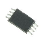
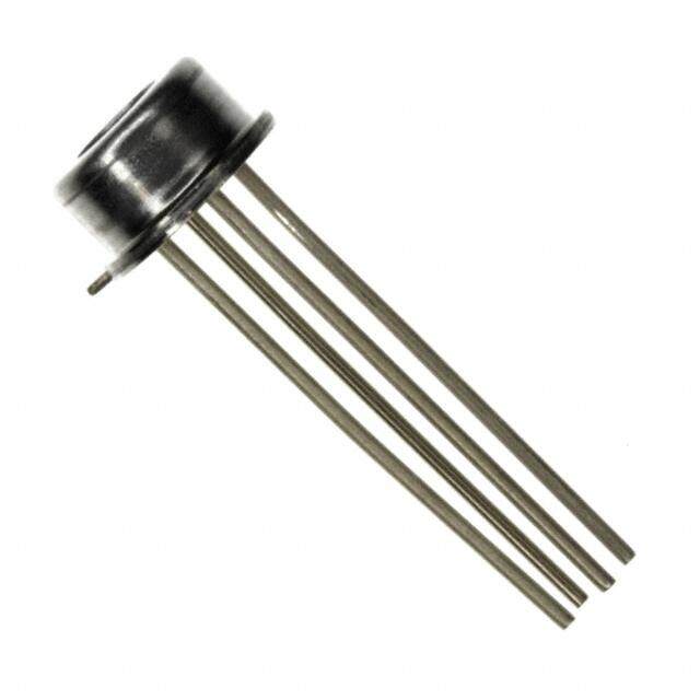
| 描述 | IC TEMP SENSOR DIGITAL 8-TSSOP板上安装温度传感器 TEMP SENSOR DIGITAL |
| 产品分类 | |
| 品牌 | NXP Semiconductors |
| 产品手册 | |
| 产品图片 |
|
| rohs | 符合RoHS无铅 / 符合限制有害物质指令(RoHS)规范要求 |
| 产品系列 | 板上安装温度传感器,NXP Semiconductors SE95DP,118- |
| 数据手册 | |
| 产品型号 | SE95DP,118 |
| PCN封装 | |
| 产品培训模块 | http://www.digikey.cn/PTM/IndividualPTM.page?site=cn&lang=zhs&ptm=25410 |
| 产品目录页面 | |
| 产品种类 | Sensors - Temperature |
| 传感器类型 | 内部 |
| 供应商器件封装 | 8-TSSOP |
| 关闭 | Shutdown |
| 其它名称 | 568-2051-1 |
| 准确性 | +/- 1 C to +/- 3 C |
| 功能 | 温度监视系统(传感器),监视器 |
| 包装 | 剪切带 (CT) |
| 商标 | NXP Semiconductors |
| 安装类型 | 表面贴装 |
| 安装风格 | SMD/SMT |
| 封装 | Reel |
| 封装/外壳 | 8-TSSOP,8-MSOP(0.118",3.00mm 宽) |
| 封装/箱体 | TSSOP-8 |
| 工作温度 | -55°C ~ 125°C |
| 工厂包装数量 | 2500 |
| 感应温度 | -55°C ~ 125°C |
| 拓扑 | ADC(三角积分型),比较器,振荡器,寄存器库 |
| 数字输出-位数 | 13 bit |
| 数字输出-总线接口 | 2-Wire, I2C, SMBus |
| 最大工作温度 | + 125 C |
| 最小工作温度 | - 55 C |
| 标准包装 | 1 |
| 温度阈值 | Programmable |
| 特色产品 | http://www.digikey.com/cn/zh/ph/NXP/I2C.html |
| 电压-电源 | 2.8 V ~ 5.5 V |
| 电源电压-最大 | 5.5 V |
| 电源电压-最小 | 2.8 V |
| 电源电流 | 7 uA |
| 精度 | ±3°C(最大) |
| 系列 | SE95 |
| 设备功能 | Sensor with Watchdog |
| 输出报警 | 无 |
| 输出类型 | Digital |
| 输出风扇 | 是 |
| 配置 | Local |
| 零件号别名 | SE95DP-T |


- 商务部:美国ITC正式对集成电路等产品启动337调查
- 曝三星4nm工艺存在良率问题 高通将骁龙8 Gen1或转产台积电
- 太阳诱电将投资9.5亿元在常州建新厂生产MLCC 预计2023年完工
- 英特尔发布欧洲新工厂建设计划 深化IDM 2.0 战略
- 台积电先进制程称霸业界 有大客户加持明年业绩稳了
- 达到5530亿美元!SIA预计今年全球半导体销售额将创下新高
- 英特尔拟将自动驾驶子公司Mobileye上市 估值或超500亿美元
- 三星加码芯片和SET,合并消费电子和移动部门,撤换高东真等 CEO
- 三星电子宣布重大人事变动 还合并消费电子和移动部门
- 海关总署:前11个月进口集成电路产品价值2.52万亿元 增长14.8%


PDF Datasheet 数据手册内容提取
SE95 Ultra high accuracy digital temperature sensor and thermal watchdog Rev. 07 — 2 September 2009 Product data sheet 1. General description The SE95 is a temperature-to-digital converter using an on-chip band gap temperature sensor and Sigma Delta analog-to-digital conversion technique. The device is also a thermal detector providing an overtemperature detection output. The SE95 contains a number of data registers accessed by a controller via the 2-wire serial I2C-bus interface: • Configuration register (Conf) to store the device settings such as sampling rate, device operation mode, OS operation mode, OS polarity, and OS fault queue • Temperature register (Temp) to store the digital Temp reading • Set-pointregisters(TosandThyst)tostoreprogrammableovertemperatureshutdown and hysteresis limits • Identification register (ID) to store manufacturer numbers The device includes an open-drain output (pin OS) which becomes active when the temperature exceeds the programmed limits. There are three selectable logic address pins (pins A2 to A0) so that eight devices can be connected on the same bus without address conflict. The SE95 can be configured for different operation conditions. It can be set in normal mode to periodically monitor the ambient temperature, or in shutdown mode to minimize power consumption. The OS output operates in either of two selectable modes: OS comparatormodeandOSinterruptmode.ItsactivestatecanbeselectedaseitherHIGH orLOW.Thefaultqueuethatdefinesthenumberofconsecutivefaultsinordertoactivate the OS output is programmable as well as the set-point limits. The temperature register always stores a 13-bit two’s complement data giving a temperature resolution of 0.03125(cid:176) C. This high temperature resolution is particularly useful in applications of measuring precisely the thermal drift or runaway. For normal operationandcompatibilitywiththeLM75A,onlythe11MSBsareread,witharesolution of0.125(cid:176) Ctoprovidetheaccuraciesspecified.TobecompatiblewiththeLM75,readonly the 9MSBs. The device is powered-up in normal operation mode with the OS in comparator mode, temperature threshold of 80(cid:176) C and hysteresis of 75(cid:176) C, so that it can be used as a stand-alone thermostat with those pre-defined temperature set points. The conversion rate is programmable, with a default of 10conversions/s.
SE95 NXP Semiconductors Ultra high accuracy digital temperature sensor and thermal watchdog 2. Features n Pin-for-pin replacement for industry standard LM75/LM75A n Specification of a single part over supply voltage from 2.8V to 5.5V n Small 8-pin package types: SO8 and TSSOP8 (MSOP8) n I2C-bus interface to 400kHz with up to 8devices on the same bus n Supply voltage from 2.8V to 5.5V n Temperature range from- 55(cid:176) C to +125(cid:176) C n 13-bit ADC that offers a temperature resolution of 0.03125(cid:176) C n Temperature accuracy of– 1(cid:176) C from- 25(cid:176) C to +100(cid:176) C n Programmable temperature threshold and hysteresis set points n Supply current of 7.0m A in shutdown mode for power conservation n Stand-alone operation as thermostat at power-up n ESDprotectionexceeds1000VforHumanBodyModel(HBM)perJESD22-A114and 150V for Machine Model (MM) per JESD22-A115 n Latch-up testing is done to JEDEC Standard JESD78 which exceeds 100mA 3. Applications n System thermal management n Personal computers n Electronics equipment n Industrial controllers 4. Ordering information Table 1. Ordering information Type Package number Temperature range Name Description Version SE95D - 55(cid:176) C to +125(cid:176) C SO8 plastic small outline package; 8 leads; bodywidth3.9mm SOT96-1 SE95DP - 55(cid:176) C to +125(cid:176) C TSSOP8 plastic thin shrink small outline package; 8 leads; SOT505-1 bodywidth3mm SE95U - 55(cid:176) C to +125(cid:176) C - wafer - SE95_7 © NXP B.V. 2009. All rights reserved. Product data sheet Rev. 07 — 2 September 2009 2 of 27
SE95 NXP Semiconductors Ultra high accuracy digital temperature sensor and thermal watchdog 5. Block diagram ADC CONTROL AND OTP CONTROL OTP SE95 8 VCC BIAS Conf Temp BAND GAP bit Tos SIGMA DELTA stream DECIMATION Thyst INTERRUPTION MODULATOR FILTER LOGIC OSCILLATOR REGISTER POR BANK 3 OS I2C-BUS INTERFACE LOGIC 5 6 7 2 1 4 A2 A1 A0 SCL SDA GND 002aae892 Fig 1. Block diagram of SE95 6. Pinning information 6.1 Pinning SDA 1 8 VCC SDA 1 8 VCC SCL 2 7 A0 SCL 2 7 A0 SE95D SE95DP OS 3 6 A1 OS 3 6 A1 GND 4 5 A2 GND 4 5 A2 002aac537 002aac536 Fig 2. Pin configuration for SO8 Fig 3. Pin configuration for TSSOP8 6.2 Pin description Table 2. Pin description Symbol Pin Description SDA 1 I2C-bus serial bidirectional data line digital I/O; open-drain SCL 2 I2C-bus serial clock digital input OS 3 overtemperature shutdown output; open-drain GND 4 ground; to be connected to the system ground A2 5 user-defined address bit2 digital input SE95_7 © NXP B.V. 2009. All rights reserved. Product data sheet Rev. 07 — 2 September 2009 3 of 27
SE95 NXP Semiconductors Ultra high accuracy digital temperature sensor and thermal watchdog Table 2. Pin description …continued Symbol Pin Description A1 6 user-defined address bit1 digital input A0 7 user-defined address bit0 digital input V 8 supply voltage CC 7. Functional description 7.1 General operation The SE95 uses the on-chip band gap sensor to measure the device temperature with a resolution of 0.03125(cid:176) C and stores the 13-bit two’s complement digital data, resulting from13-bitanalogtodigitalconversion,intoregisterTemp.RegisterTempcanbereadat any time by a controller on the I2C-bus. Reading temperature data does not affect the conversion in progress during the read operation. The device can be set to operate in either mode: normal or shutdown mode. In normal operation mode, by default, the temperature-to-digital conversion is executed every 100ms and register Temp is updated at the end of each conversion. In shutdown mode, the device becomes idle, data conversion is disabled and register Temp holds the latest result;however,thedeviceI2C-businterfaceisstillactiveandregisterwrite/readoperation can be performed. The device operation mode is controlled by programming bit SHUTDOWN of register Conf. The temperature conversion is initiated when the device is powered up or returned to normal mode from shutdown mode. Inaddition,attheendofeachconversioninnormalmode,thetemperaturedata(orTemp) in register Temp is automatically compared with the overtemperature shutdown threshold data (or Tos) stored in register Tos, and the hysteresis data (or Thyst) stored in register Thyst,inordertosetthestateofthedeviceOSoutputaccordingly.TheregistersTosand Thyst are write/read capable, and both operate with 9-bit two’s complement digital data. Tomatchwiththis9-bitoperation,registerTempusesonlythe9MSBbitsofits13-bitdata for the comparison. Thedevicetemperatureconversionrateisprogrammableandcanbechosentobeoneof the four values: 0.125, 1.0, 10, and 30 conversions/s. The default conversion rate is 10conversions/s. Furthermore, the conversion rate is selected by programming bits RATEVAL[1:0] of register Conf as shown inTable6. Note that the average supply current as well as the device power consumption increase with the conversion rate. The way that the OS output responds to the comparison operation depends upon the OS operation mode selected by configuration bitOS_COMP_INT, and the user-defined fault queue defined by configuration bitsOS_F_QUE[1:0]. In OS comparator mode, the OS output behaves like a thermostat. It becomes active whenthetemperatureexceedsT ,andisresetwhenthetemperaturedropsbelowT . os hyst Reading the device registers or putting the device into shutdown mode does not change thestateoftheOSoutput.TheOSoutputinthiscasecanbeusedtocontrolcoolingfans or thermal switches. SE95_7 © NXP B.V. 2009. All rights reserved. Product data sheet Rev. 07 — 2 September 2009 4 of 27
SE95 NXP Semiconductors Ultra high accuracy digital temperature sensor and thermal watchdog In OS interrupt mode, the OS output is used for thermal interruption. When the device is powered-up,theOSoutputisfirstactivatedonlywhenTempexceedsT ;thenitremains os activeindefinitelyuntilbeingresetbyareadofanyregister.OncetheOSoutputhasbeen activatedbycrossingT andthenreset,itcanbeactivatedagainonlywhenTempdrops os below T ; then again, it remains active indefinitely until being reset by a read of any hyst register. The OS interrupt operation would be continued in this sequence: T trip, reset, os T trip, reset, T trip, reset, T trip, reset, and etc. Putting the device into shutdown hyst os hyst mode also resets the OS output. In both cases, comparator mode and interrupt mode, the OS output is activated only if a number of consecutive faults, defined by the device fault queue, has been met. The fault queueisprogrammableandstoredinbitsOS_F_QUE[1:0],ofregisterConf.Also,theOS output active state is selectable as HIGH or LOW by setting accordingly the bit OS_POL of register Conf. At power-up, the device is put into normal operation mode, register Tos is set to 80(cid:176) C, registerThystissetto75(cid:176) C,OSactivestateisselectedLOWandthefaultqueueisequal to1. The data reading of register Temp is not available until the first conversion is completed in about33ms. The OS response to the temperature is illustrated inFigure4. Tos Thyst reading temperature limits OS RESET OS ACTIVE OS output in comparator mode OS RESET (1) (1) (1) OS ACTIVE OS output in interrupt mode 001aad623 (1) OS is reset by either reading register or putting the device in shutdown mode. Assumed that the fault queue is met at each T and T crossing point. os hyst Fig 4. OS response to temperature SE95_7 © NXP B.V. 2009. All rights reserved. Product data sheet Rev. 07 — 2 September 2009 5 of 27
SE95 NXP Semiconductors Ultra high accuracy digital temperature sensor and thermal watchdog 7.2 OS output and polarity The OS output is an open-drain output and its state represents results of the device watchdog operation as described inSection7.1. In order to observe this output state, an external pull-up resistor is needed. The resistor should be as large as possible, up to 200kW ,tominimizetheTempreadingerrorduetointernalheatingbythehighOSsinking current. The OS output active state can be selected as HIGH or LOW by programming bit OS_POL of register Conf: setting bit OS_POL to logic 1 selects OS active HIGH and settingtologic0setsOSactiveLOW.Atpower-up,bitOS_POLisequaltologic0andthe OS active state is LOW. 7.3 OS comparator and interrupt modes As described inSection7.1, the OS output responds to the result of the comparison between register Temp data and the programmed limits, in registers Tos and Thyst, in different ways depending on the selected OS mode: OS comparator or OS interrupt. The OS mode is selected by programming bit OS_COMP_INT of register Conf: setting bit OS_COMP_INTtologic1selectstheOSinterruptmode,andsettingtologic0selectsthe OS comparator mode. At power-up, bit OS_COMP_INT is equal to logic 0 and the OS comparator is selected. The main difference between the two modes is that in OS comparator mode, the OS output becomes active when Temp has exceeded T and reset when Temp has dropped os belowT ,readingaregisterorputtingthedeviceintoshutdownmodedoesnotchange hyst the state of the OS output; while in OS interrupt mode, once it has been activated either byexceedingT ordroppingbelowT ,theOSoutputwillremainactiveindefinitelyuntil os hyst readingaregisterorputtingthedeviceintoshutdownmodeoccurs,thentheOSoutputis reset. Temperature limits T and T must be selected so that T > T . Otherwise, the OS os hyst os hyst output state will be undefined. 7.4 OS fault queue Fault queue is defined as the number of faults that must occur consecutively to activate the OS output. It is provided to avoid false tripping due to noise. Because faults are determined at the end of data conversions, fault queue is also defined as the number of consecutive conversions returning a temperature trip. The value of fault queue is selectable by programming the two bits OS_F_QUE[1:0] in register Conf. Notice that the programmed data and the fault queue value are not the same.Table3 shows the one-to-onerelationshipbetweenthem.Atpower-up,faultqueuedata=00andfaultqueue value=1. Table 3. Fault queue table Fault queue data Fault queue value OS_F_QUE[1] OS_F_QUE[0] Decimal 0 0 1 0 1 2 1 0 4 1 1 6 SE95_7 © NXP B.V. 2009. All rights reserved. Product data sheet Rev. 07 — 2 September 2009 6 of 27
SE95 NXP Semiconductors Ultra high accuracy digital temperature sensor and thermal watchdog 7.5 Shutdown mode ThedeviceoperationmodeisselectedbyprogrammingbitSHUTDOWNofregisterConf. Setting bit SHUTDOWN to logic 1 will put the device into shutdown mode. Resetting bit SHUTDOWN to logic 0 will return the device to normal mode. In shutdown mode, the device draws a small current of approximately 7.5m A and the power dissipation is minimized; the temperature conversion stops, but the I2C-bus interface remains active and register write/read operation can be performed. If the OS output is in comparator mode, then it remains unchanged. In interrupt mode, the OS output is reset. 7.6 Power-up default and power-on reset The SE95 always powers-up in its default state with: • Normal operation mode • OS comparator mode • T = 80(cid:176) C os • T = 75(cid:176) C hyst • OS output active state is LOW • Pointer value is logic 0 When the power supply voltage is dropped below the device power-on reset level of approximately 1.9V (POR) and then rises up again, the device will be reset to its default condition as listed above. 8. I2C-bus serial interface The SE95 can be connected to a compatible 2-wire serial interface I2C-bus as a slave deviceunderthecontrolofacontrollerormasterdevice,usingtwodeviceterminals,SCL and SDA. The controller must provide the SCL clock signal and write/read data to and from the device through the SDA terminal. Note that if the I2C-bus common pull-up resistorshavenotbeeninstalledasrequiredforI2C-bus,thenanexternalpull-upresistor, approximately 10kW , is needed for each of these two terminals. The bus communication protocols are described inSection 8.7 “Protocols for writing and reading the registers”. 8.1 Slave address The SE95 slave address on the I2C-bus is partially defined by the logic applied to the device address pins A2, A1 and A0. Each pin is typically connected either to GND for logic0, or to V for logic1. These pins represent the three LSB bits of the device 7-bit CC address. The other four MSB bits of the address data are preset to 1001 by hard wiring inside the SE95.Table4 shows the device's complete address and indicates that up to 8devices can be connected to the same bus without address conflict. Because the input pinsSCL,SDAandA2toA0,arenotinternallybiased,itisimportantthattheyshouldnot be left floating in any application. 0ChisareservedaddressforSMBusAlertResponseAddress(ARA).Thisisanoptional commandfromtheSMBusspecificationtoallowSMBusdevicestorespondtoanSMBus master with their slave device if they are generating an interrupt. The SE95 will send a SE95_7 © NXP B.V. 2009. All rights reserved. Product data sheet Rev. 07 — 2 September 2009 7 of 27
SE95 NXP Semiconductors Ultra high accuracy digital temperature sensor and thermal watchdog falsealertiftheaddress0ChissentandcannotbeactiveontheI2C-busifthisaddressis used.ConsiderusingtheSE98sinceitsupportsSMBusARAaswellastime-outfeatures and provides– 1(cid:176) C accuracy. Table 4. Address table MSB LSB 1 0 0 1 A2 A1 A0 8.2 Register list The SE95 contains 7 data registers. The registers can be 1byte or 2bytes wide, and are defined inTable5. The registers are accessed by the value in the content of the pointer register during I2C-bus communication. The types of registers are: read only, read/write, and reserved for manufacturer use. Note that when reading a two-byte register, the host must provide enough clock pulses as required by the I2C-bus protocol (seeSection8.7) for the device to completely return both data bytes. Otherwise the device may hold the SDA line in LOW state, resulting in a bus hang condition. Table 5. Register table Register Pointer R/W POR Description name value state Conf 01h R/W 00h configurationregister:containsasingle8-bitdatabyte; to set an operating condition Temp 00h read N/A temperature register: contains two 8-bit data bytes; to only store the measured Temp Tos 03h R/W 5000h overtemperatureshutdownthresholdregister:contains two 8-bit data bytes; to store the overtemperature shutdown limit; default T =80(cid:176) C os Thyst 02h R/W 4B00h hysteresis register: contains two 8-bit data bytes; to store the hysteresis limit; bit 7 to bit 0 are also used in OTP (One Time Programmable) test mode to supply OTP write data; default T =75(cid:176) C hyst ID 05h read A1h identification register: contains a single 8-bit data byte only for the manufacturer ID code Reserved 04h N/A N/A reserved Reserved 06h N/A N/A reserved 8.3 Register pointer The register pointer or pointer byte is an 8-bit data byte that is equivalent to the register command in the I2C-bus definitions and is used to identify the device register to be accessed for a write or read operation. Its values are listed as pointer values inTable5. For the device register I2C-bus communication, the pointer byte may or may not need to be included within the command as illustrated in the I2C-bus protocol figures in Section8.7. The command statements for writing data to a register must always include the pointer byte; while the command statements for reading data from a register may or may not includeit.Toreadaregisterthatisdifferentfromtheonethathasbeenrecentlyread,the pointerbytemustbeincluded.However,tore-readaregisterthathasbeenrecentlyread, the pointer byte may not have to be included in the reading. SE95_7 © NXP B.V. 2009. All rights reserved. Product data sheet Rev. 07 — 2 September 2009 8 of 27
SE95 NXP Semiconductors Ultra high accuracy digital temperature sensor and thermal watchdog At power-up, the pointer value is preset to logic0 for register Temp; users can then read the temperature without specifying the pointer byte. 8.4 Configuration register The Configuration (Conf) register is a read/write register and contains an 8-bit non-complement data byte that is used to configure the device for different operating conditions.Table6 shows the bit assignments of this register. Table 6. Conf register Legend: * = default value. Bit Symbol Access Value Description 7 reserved R/W 0* reserved for manufacturer’s use 6 and 5 RATEVAL[1:0] R/W sets the conversion rate 00* 10 conversion/s 01 0.125 conversion/s 10 1 conversion/s 11 30 conversion/s 4 and 3 OS_F_QUE[1:0] R/W OS fault queue programming 00* queue value = 1 01 queue value = 2 10 queue value = 4 11 queue value = 6 2 OS_POL R/W OS polarity selection 0* OS active LOW 1 OS active HIGH 1 OS_COMP_INT R/W OS operation mode selection 0* OS comparator 1 OS interrupt 0 SHUTDOWN R/W 0 operation mode 0* normal 1 shutdown 8.5 Temperature register The Temperature (Temp) register holds the digital result of temperature measurement or monitor at the end of each analog to digital conversion. This register is read only and contains two 8-bit data bytes consisting of one Most Significant Byte (MSByte) and one LeastSignificantByte(LSByte).However,only13bitsofthosetwobytesareusedtostore the Temp data in two’s complement format with the resolution of 0.03125(cid:176) C.Table7 shows the bit arrangement of the Temp data in the data bytes. Table 7. Temp register MSByte LSByte 7 6 5 4 3 2 1 0 7 6 5 4 3 2 1 0 D15 D14 D13 D12 D11 D10 D9 D8 D7 D6 D5 D4 D3 D2 D1 D0 SE95_7 © NXP B.V. 2009. All rights reserved. Product data sheet Rev. 07 — 2 September 2009 9 of 27
SE95 NXP Semiconductors Ultra high accuracy digital temperature sensor and thermal watchdog When reading register Temp, all 16bits of the two data bytes (MSByte and LSByte) must becollectedandthenthetwo’scomplementdatavalueaccordingtothedesiredresolution must be selected for the temperature calculation.Table8 shows the example for 11-bit two’s complement data value,Table9 shows the example for 13-bit two’s complement data value. Table 8. Example 11-bit two’s complement Temp register MSByte LSByte 7 6 5 4 3 2 1 0 7 6 5 4 3 2 1 0 D10 D9 D8 D7 D6 D5 D4 D3 D2 D1 D0 X X X X X Table 9. Example 13-bit two’s complement register MSByte LSByte 7 6 5 4 3 2 1 0 7 6 5 4 3 2 1 0 D12 D11 D10 D9 D8 D7 D6 D5 D4 D3 D2 D1 D0 X X X When converting into the temperature the proper resolution must be used as listed in Table10 using either one of these two formulae: 1. If the Temp data MSB=0, then: Temp ((cid:176) C) = +(Temp data)· value resolution 2. IftheTempdataMSB=1,then:Temp((cid:176) C)=- (two’scomplementTempdata)· value resolution Table 10. Temp data and Temp value resolution Data resolution Value resolution 8 bit 1.0(cid:176) C 9 bit 0.5(cid:176) C 10 bit 0.25(cid:176) C 11 bit 0.125(cid:176) C 12 bit 0.0625(cid:176) C 13 bit 0.03125(cid:176) C Table11 shows some examples of the results for the 11-bit calculations. Table 11. Temp register value 11-bit binary Hexadecimal value Decimal value Value (two’scomplement) 011 1111 1000 3F8 1016 +127.000(cid:176) C 011 1111 0111 3F7 1015 +126.875(cid:176) C 011 1111 0001 3F1 1009 +126.125(cid:176) C 011 1110 1000 3E8 1000 +125.000(cid:176) C 000 1100 1000 0C8 200 +25.000(cid:176) C 000 0000 0001 001 1 +0.125(cid:176) C 000 0000 0000 000 0 0.000(cid:176) C 111 1111 1111 7FF - 1 - 0.125(cid:176) C 111 0011 1000 738 - 200 - 25.000(cid:176) C 110 0100 1001 649 - 439 - 54.875(cid:176) C 110 0100 1000 648 - 440 - 55.000(cid:176) C SE95_7 © NXP B.V. 2009. All rights reserved. Product data sheet Rev. 07 — 2 September 2009 10 of 27
SE95 NXP Semiconductors Ultra high accuracy digital temperature sensor and thermal watchdog Obviously, for 9-bit Temp data application in replacing the industry standard LM75, just use only 9MSB bits of the two bytes and disregard 7LSB of the LSByte. The 9-bit Temp data with 0.5(cid:176) C resolution of the SE95 is defined exactly in the same way as for the standard LM75 and it is here similar to the Tos and Thyst registers. 8.6 Overtemperature shutdown threshold and hysteresis registers Thesetworegisters,arewrite/readregisters,andalsocalledset-pointregisters.Theyare used to store the user-defined temperature limits, called overtemperature shutdown threshold(Tos)andhysteresistemperature(Thyst),forthedevicewatchdogoperation.At the end of each conversion the Temp data will be compared with the data stored in these two registers in order to set the state of the device OS output; seeSection7.1. Eachoftheset-pointregisterscontainstwo8-bitdatabytesconsistingofoneMSByteand one LSByte the same as register Temp. However, only 9bits of the two bytes are used to storetheset-pointdataintwo’scomplementformatwiththeresolutionof0.5(cid:176) C.Table12 andTable13 show the bit arrangement of the Tos data and Thyst data in the data bytes. Notice that because only 9-bit data are used in the set-point registers, the device uses only the 9MSB of the Temp data for data comparison. Table 12. Tos register MSByte LSByte 7 6 5 4 3 2 1 0 7 6 5 4 3 2 1 0 D8 D7 D6 D5 D4 D3 D2 D1 D0 X X X X X X X Table 13. Thyst register MSByte LSByte 7 6 5 4 3 2 1 0 7 6 5 4 3 2 1 0 D8 D7 D6 D5 D4 D3 D2 D1 D0 X X X X X X X Whenaset-pointregisterisread,all16bitsareprovidedtothebusandmustbecollected by the controller to complete the bus operation. However, only the 9most significant bits should be used and the 7LSB of the LSByte are equal to zero and should be ignored. Table14 shows examples of the limit data and value. Table 14. Tos and Thyst register 11-bit binary Hexadecimal value Decimal value Value (two’scomplement) 0 1111 1010 0FA 250 125.0(cid:176) C 0 0011 0010 032 50 25.0(cid:176) C 0 0000 0001 001 1 0.5(cid:176) C 0 0000 0000 000 0 0.0(cid:176) C 1 1111 1111 1FF - 1 - 0.5(cid:176) C 1 1100 1110 1CE - 50 - 25.0(cid:176) C 1 1001 0010 192 - 110 - 55.0(cid:176) C SE95_7 © NXP B.V. 2009. All rights reserved. Product data sheet Rev. 07 — 2 September 2009 11 of 27
SE95 NXP Semiconductors Ultra high accuracy digital temperature sensor and thermal watchdog 8.7 Protocols for writing and reading the registers The communication between the host and the SE95 must follow the rules strictly as defined by the I2C-bus management. The protocols for SE95 register read/write operations are illustrated inFigure5 toFigure10 together with the following definitions: 1. Beforeacommunication,theI2C-busmustbefreeornotbusy.ItmeansthattheSCL and SDA lines must both be released by all devices on the bus, and they become HIGH by the bus pull-up resistors. 2. The host must provide SCL clock pulses necessary for the communication. Data is transferred in a sequence of 9SCL clock pulses for every 8-bit data byte followed by 1-bit status of the acknowledgement. 3. During data transfer, except the START and STOP signals, the SDA signal must be stable while the SCL signal is HIGH. It means that the SDA signal can be changed only during the LOW duration of the SCL line. 4. S: START signal, initiated by the host to start a communication, the SDA goes from HIGH-to-LOW while the SCL is HIGH. 5. RS: RE-START signal, same as the START signal, to start a read command that follows a write command. 6. P: STOP signal, generated by the host to stop a communication, the SDA goes from LOW-to-HIGH while the SCL is HIGH. The bus becomes free thereafter. 7. W: write bit, when the write/read bit is in a write command. 8. R: read bit, when the write/read bit is logic 1 in a read command. 9. A: device acknowledge bit, returned by the SE95. It is logic0 if the device works properly and logic1 if not. The host must release the SDA line during this period in order to give the device the control on the SDA line. 10. A’: master acknowledge bit, not returned by the device, but set by the master or host in reading 2-byte data. During this clock period, the host must set the SDA line to LOW in order to notify the device that the first byte has been read for the device to provide the second byte onto the bus. 11. NA: not-acknowledge bit. During this clock period, both the device and host release the SDA line at the end of a data transfer, the host is then enabled to generate the stop signal. 12. In a write protocol, data is sent from the host to the device and the host controls the SDA line, except during the clock period when the device sends the device acknowledgement signal to the bus. 13. Inareadprotocol,dataissenttothebusbythedeviceandthehostmustreleasethe SDAlineduringthetimethatthedeviceisprovidingdataontothebusandcontrolling the SDA line, except during the clock period when the master sends the master acknowledgement signal to the bus. SE95_7 © NXP B.V. 2009. All rights reserved. Product data sheet Rev. 07 — 2 September 2009 12 of 27
SE95 NXP Semiconductors Ultra high accuracy digital temperature sensor and thermal watchdog 1 2 3 4 5 6 7 8 9 1 2 3 4 5 6 7 8 9 1 2 3 4 5 6 7 8 9 SCL SDA S 1 0 0 1 A2 A1 A0 W A 0 0 0 0 0 0 0 1 A 0 0 0 D4 D3 D2 D1 D0 A P device address pointer byte configuration data byte START write device device STOP acknowledge acknowledge device acknowledge 001aad624 Fig 5. Write configuration register (1-byte data) 1 2 3 4 5 6 7 8 9 1 2 3 4 5 6 7 8 9 SCL (next) SDA S 1 0 0 1 A2 A1 A0 W A 0 0 0 0 0 0 0 1 A RS (next) device address pointer byte START write device RE-START acknowledge device acknowledge 1 2 3 4 5 6 7 8 9 1 2 3 4 5 6 7 8 9 SCL (cont.) SDA (cont.) 1 0 0 1 A2 A1 A0 R A D7 D6 D5 D4 D3 D2 D1 D0 NA P device address data byte from device read master not STOP acknowledged device acknowledge 001aad625 Fig 6. Read configuration register including pointer byte (1-byte data) 1 2 3 4 5 6 7 8 9 1 2 3 4 5 6 7 8 9 SCL SDA S 1 0 0 1 A2 A1 A0 R A D7 D6 D5 D4 D3 D2 D1 D0 NA P device address data byte from device START read master not STOP acknowledged device acknowledge 001aad626 Fig 7. Read configuration register with preset pointer (1-byte data) SE95_7 © NXP B.V. 2009. All rights reserved. Product data sheet Rev. 07 — 2 September 2009 13 of 27
SE95 NXP Semiconductors Ultra high accuracy digital temperature sensor and thermal watchdog 1 2 3 4 5 6 7 8 9 1 2 3 4 5 6 7 8 9 SCL (next) SDA S 1 0 0 1 A2 A1 A0 W A 0 0 0 0 0 0 P1 P0 A (next) device address pointer byte START write device acknowledge device acknowledge 1 2 3 4 5 6 7 8 9 1 2 3 4 5 6 7 8 9 SCL (cont.) SDA (cont.) D7 D6 D5 D4 D3 D2 D1 D0 A D7 D6 D5 D4 D3 D2 D1 D0 A P ms byte data ls byte data device STOP acknowledge device acknowledge 001aad627 Fig 8. Write Tos or Thyst register (2-byte data) 1 2 3 4 5 6 7 8 9 1 2 3 4 5 6 7 8 9 0 SCL (next) SDA S 1 0 0 1 A2 A1 A0 W A 0 0 0 0 0 0 P1 P0 A RS (next) device address pointer byte START write device RE-START acknowledge device acknowledge 1 2 3 4 5 6 7 8 9 1 2 3 4 5 6 7 8 9 1 2 3 4 5 6 7 8 9 SCL (cont) SDA (cont) 1 0 0 1 A2 A1 A0 R A D7 D6 D5 D4 D3 D2 D1 D0 A4 D7 D6 D5 D4 D3 D2 D1 D0 NA P device address ms byte from device ls byte from device read master master not STOP acknowledge acknowledged device acknowledge 001aad628 Fig 9. Read Temp, Tos or Thyst register including pointer byte (2-byte data) 1 2 3 4 5 6 7 8 9 1 2 3 4 5 6 7 8 9 1 2 3 4 5 6 7 8 9 SCL SDA S 1 0 0 1 A2 A1 A0 R A D7 D6 D5 D4 D3 D2 D1 D0 A4 D7 D6 D5 D4 D3 D2 D1 D0 NA P device address ms byte from device ls byte from device START read master master not STOP acknowledge acknowledged device acknowledge 001aad629 Fig 10. Read Temp, Tos or Thyst register with preset pointer (2-byte data) SE95_7 © NXP B.V. 2009. All rights reserved. Product data sheet Rev. 07 — 2 September 2009 14 of 27
SE95 NXP Semiconductors Ultra high accuracy digital temperature sensor and thermal watchdog 9. Limiting values Table 15. Limiting values In accordance with the Absolute Maximum Rating System (IEC 60134). Symbol Parameter Conditions Min Max Unit V supply voltage - 0.3 +6.0 V CC V input voltage on pin SCL - 0.3 +6.0 V I(SCL) V input voltage on pin SDA - 0.3 +6.0 V I(SDA) V input voltage on pin A0 - 3.0 V +0.3 V I(A0) CC V input voltage on pin A1 - 3.0 V +0.3 V I(A1) CC V input voltage on pin A2 - 3.0 V +0.3 V I(A2) CC I input current on input pins - 5.0 +5.0 mA I(PIN) I output current on pin OS - 10.0 mA O(OS) V output voltage on pin OS - 0.3 +6.0 V O(OS) V electrostatic discharge human body model - 1000 V ESD voltage machine model - 150 V T storage temperature - 65 +150 (cid:176) C stg T junction temperature - 150 (cid:176) C j 10. Recommended operating conditions Table 16. Recommended operating characteristics Symbol Parameter Conditions Min Typ Max Unit V supply voltage 2.8 - 5.5 V CC T ambient temperature - 55 - +125 (cid:176) C amb SE95_7 © NXP B.V. 2009. All rights reserved. Product data sheet Rev. 07 — 2 September 2009 15 of 27
SE95 NXP Semiconductors Ultra high accuracy digital temperature sensor and thermal watchdog 11. Static characteristics Table 17. Static characteristics V = 2.8V to 5.5V, T =- 55(cid:176) C to +125(cid:176) C; unless otherwise specified. CC amb Symbol Parameter Conditions Min Typ[1] Max Unit T temperature accuracy V =2.8V to 3.6V [2] acc CC T =- 25(cid:176) C to +100(cid:176) C - 1.0 - +1.0 (cid:176) C amb T =- 55(cid:176) C to +125(cid:176) C - 2.0 - +2.0 (cid:176) C amb V =3.6V to 5.5V [2] CC T =- 25(cid:176) C to +100(cid:176) C - 2 - +2 (cid:176) C amb T =- 55(cid:176) C to +125(cid:176) C - 3 - +3 (cid:176) C amb T temperature resolution 11-bit digital temperature data - 0.125 - (cid:176) C res t temperature conversion time normal mode - 33 - ms conv(T) I supply current normal mode: I2C-bus inactive - 150 - m A CC normal mode: I2C-bus active - - 1.0 mA shutdown mode - 7.5 - m A V HIGH-level input voltage digital pins [3] 0.7V - V +0.3 V IH CC CC V LOW-level input voltage digital pins [3] - 0.3 - +0.3V V IL CC V hysteresis of input voltage pins SCL and SDA - 300 - mV I(hys) pins A2 to A0 - 300 - mV I HIGH-level input current digital pins; V =V [3] - 1.0 - +1.0 m A IH IN CC I LOW-level input current digital pins; V =0V [3] - 1.0 - +1.0 m A IL IN V LOW-level output voltage pins SDA and OS; I =3mA - - 0.4 V OL OL I =4mA - - 0.8 V OL I output leakage current pins SDA and OS; V =V - - 10 m A LO OH CC V power-on reset voltage V supply below which the 1.0 - 2.5 V POR CC logic is reset OSQ OS fault queue programmable [4] 1 - 6 T overtemperature shutdown default value - 80 - (cid:176) C os threshold f sampling rate programmable 0.125 10 30 sample/s sam T hysteresis temperature default value - 75 - (cid:176) C hyst C input capacitance digital pins - 20 - pF i [1] Typical values are at V =3.3V and T =25(cid:176) C. CC amb [2] Assumes a minimum 11-bit temperature reading. [3] The digital pins are pin SCL, SDA and A2 to A0. [4] Device analog-to-digital conversion. SE95_7 © NXP B.V. 2009. All rights reserved. Product data sheet Rev. 07 — 2 September 2009 16 of 27
SE95 NXP Semiconductors Ultra high accuracy digital temperature sensor and thermal watchdog 12. Dynamic characteristics Table 18. Dynamic characteristics[1] V = 2.8V to 5.5V, T =- 55(cid:176) C to +125(cid:176) C; unless otherwise specified. CC amb Symbol Parameter Conditions Min Typ Max Unit T SCL clock period seeFigure11 2.5 - - m s CLK t HIGH period of the SCL clock 0.6 - - m s (SCL)H t LOW period of the SCL clock 1.3 - - m s (SCL)L t hold time (repeated) START condition 100 - - ns HD;STA t data set-up time 100 - - ns SU;DAT t data hold time 0 - - ns HD;DAT t set-up time for STOP condition 100 - - ns SU;STO t fall time pins SDA and OS; - 250 - ns f C =400pF; I =3mA L OL [1] These specifications are guaranteed by design and not tested in production. SDA tLOW tf tf tSU;DAT tHD;STA SCL tHD;STA tHD;DAT tHIGH tSU;STO s sr p s 001aad616 Fig 11. Timing diagram SE95_7 © NXP B.V. 2009. All rights reserved. Product data sheet Rev. 07 — 2 September 2009 17 of 27
SE95 NXP Semiconductors Ultra high accuracy digital temperature sensor and thermal watchdog 13. Performance curves 001aad617 001aad618 25 300 ICC(SD) (m A2)0 VCC = 5.5 V (ImCAC) VCC = 5.5 V 3.9 V 200 3.3 V 15 2.8 V 3.9 V 10 3.3 V 100 2.8 V 5 0 0 - 50 - 25 0 25 50 75 100 125 - 50 - 25 0 25 50 75 100 125 T ((cid:176)C) T ((cid:176)C) Fig 12. Shutdown supply current as a function of Fig 13. TypicalnormalI2C-businactivesupplycurrent temperature as a function of temperature 001aad619 001aad620 300 0.25 30 conversions/s VOL(SDA) (ImCAC) (V0.)20 VCC = 23..83 VV 3.9 V 200 10 conversions/s 0.15 5.5 V 1 conversions/s 0.125 conversions/s 0.10 100 0.05 0 0 - 50 - 25 0 25 50 75 100 125 - 50 - 25 0 25 50 75 100 125 T ((cid:176)C) T ((cid:176)C) Fig 14. TypicalnormalI2C-businactivesupplycurrent Fig 15. Typical SDA V as a function of temperature OL as a function of temperature 001aad621 001aad622 25 25 tconv(T) VOL(OS) (ms) (V) 20 20 VCC = 2.8 V 3.3 V 3.9 V 15 15 5.5 V 10 10 5 5 0 0 - 50 - 25 0 25 50 75 100 125 - 50 - 25 0 25 50 75 100 125 T ((cid:176)C) T ((cid:176)C) Fig 16. Typical conversion time as a function of Fig 17. Typical OS V as a function of temperature OL temperature SE95_7 © NXP B.V. 2009. All rights reserved. Product data sheet Rev. 07 — 2 September 2009 18 of 27
SE95 NXP Semiconductors Ultra high accuracy digital temperature sensor and thermal watchdog 14. Application information The SE95 is sensitive to power supplies with ramp-up time£ 2ms and could NACK or hang the I2C-bus. In most applications the SE95 will function properly since power supplies have a >2ms ramp-up time. If the power supply ramp-up time is£ 2ms, use an RC network with R=300W and C=10m F, as shown inFigure18, to add about 3ms to the ramp-up time. The 10m F capacitor is the same as the bypass capacitor that is typically used to prevent fluctuations on the power supply. The 300W resistor will reduce thesupplyvoltagebyabout45mVsincetheSE95supplycurrentisabout150m A.Ensure the SE95 is the only device connected to the end of 300W resistor since additional devices would draw more current and cause a larger voltage drop across the resistor. power supply 300 W power supply 10 kW 10 m F VCC SCL I2C-bus SDA SE95 OS detector or interrupt line A2 digital logic A1 or tie to A0 VCC or GND GND 002aae891 Fig 18. Typical application circuit SE95_7 © NXP B.V. 2009. All rights reserved. Product data sheet Rev. 07 — 2 September 2009 19 of 27
SE95 NXP Semiconductors Ultra high accuracy digital temperature sensor and thermal watchdog 15. Package outline SO8: plastic small outline package; 8 leads; body width 3.9 mm SOT96-1 D E A X c y HE v M A Z 8 5 Q A2 A1 (A 3 ) A pin 1 index q Lp 1 4 L e w M detail X bp 0 2.5 5 mm scale DIMENSIONS (inch dimensions are derived from the original mm dimensions) UNIT mAax. A1 A2 A3 bp c D(1) E(2) e HE L Lp Q v w y Z(1) q 0.25 1.45 0.49 0.25 5.0 4.0 6.2 1.0 0.7 0.7 mm 1.75 0.25 1.27 1.05 0.25 0.25 0.1 0.10 1.25 0.36 0.19 4.8 3.8 5.8 0.4 0.6 0.3 8o 0.010 0.057 0.019 0.0100 0.20 0.16 0.244 0.039 0.028 0.028 0o inches 0.069 0.01 0.05 0.041 0.01 0.01 0.004 0.004 0.049 0.014 0.0075 0.19 0.15 0.228 0.016 0.024 0.012 Notes 1. Plastic or metal protrusions of 0.15 mm (0.006 inch) maximum per side are not included. 2. Plastic or metal protrusions of 0.25 mm (0.01 inch) maximum per side are not included. OUTLINE REFERENCES EUROPEAN ISSUE DATE VERSION IEC JEDEC JEITA PROJECTION 99-12-27 SOT96-1 076E03 MS-012 03-02-18 Fig 19. Package outline SOT96-1 (SO8) SE95_7 © NXP B.V. 2009. All rights reserved. Product data sheet Rev. 07 — 2 September 2009 20 of 27
SE95 NXP Semiconductors Ultra high accuracy digital temperature sensor and thermal watchdog TSSOP8: plastic thin shrink small outline package; 8 leads; body width 3 mm SOT505-1 D E A X c y HE v M A Z 8 5 A2 A1 (A3) A pin 1 index q Lp L 1 4 detail X e w M bp 0 2.5 5 mm scale DIMENSIONS (mm are the original dimensions) UNIT mAax. A1 A2 A3 bp c D(1) E(2) e HE L Lp v w y Z(1) q mm 1.1 0.15 0.95 0.25 0.45 0.28 3.1 3.1 0.65 5.1 0.94 0.7 0.1 0.1 0.1 0.70 6(cid:176) 0.05 0.80 0.25 0.15 2.9 2.9 4.7 0.4 0.35 0(cid:176) Notes 1. Plastic or metal protrusions of 0.15 mm maximum per side are not included. 2. Plastic or metal protrusions of 0.25 mm maximum per side are not included. OUTLINE REFERENCES EUROPEAN ISSUE DATE VERSION IEC JEDEC JEITA PROJECTION 99-04-09 SOT505-1 03-02-18 Fig 20. Package outline SOT505-1 (TSSOP8) SE95_7 © NXP B.V. 2009. All rights reserved. Product data sheet Rev. 07 — 2 September 2009 21 of 27
SE95 NXP Semiconductors Ultra high accuracy digital temperature sensor and thermal watchdog 16. Soldering of SMD packages Thistextprovidesaverybriefinsightintoacomplextechnology.Amorein-depthaccount of soldering ICs can be found in Application NoteAN10365 “Surface mount reflow soldering description”. 16.1 Introduction to soldering Soldering is one of the most common methods through which packages are attached to PrintedCircuitBoards(PCBs),toformelectricalcircuits.Thesolderedjointprovidesboth the mechanical and the electrical connection. There is no single soldering method that is ideal for all IC packages. Wave soldering is often preferred when through-hole and Surface Mount Devices (SMDs) are mixed on one printed wiring board; however, it is not suitable for fine pitch SMDs. Reflow soldering is ideal for the small pitches and high densities that come with increased miniaturization. 16.2 Wave and reflow soldering Wavesolderingisajoiningtechnologyinwhichthejointsaremadebysoldercomingfrom a standing wave of liquid solder. The wave soldering process is suitable for the following: • Through-hole components • Leaded or leadless SMDs, which are glued to the surface of the printed circuit board Not all SMDs can be wave soldered. Packages with solder balls, and some leadless packages which have solder lands underneath the body, cannot be wave soldered. Also, leaded SMDs with leads having a pitch smaller than ~0.6mm cannot be wave soldered, due to an increased probability of bridging. The reflow soldering process involves applying solder paste to a board, followed by component placement and exposure to a temperature profile. Leaded packages, packages with solder balls, and leadless packages are all reflow solderable. Key characteristics in both wave and reflow soldering are: • Board specifications, including the board finish, solder masks and vias • Package footprints, including solder thieves and orientation • The moisture sensitivity level of the packages • Package placement • Inspection and repair • Lead-free soldering versus SnPb soldering 16.3 Wave soldering Key characteristics in wave soldering are: • Process issues, such as application of adhesive and flux, clinching of leads, board transport, the solder wave parameters, and the time during which components are exposed to the wave • Solder bath specifications, including temperature and impurities SE95_7 © NXP B.V. 2009. All rights reserved. Product data sheet Rev. 07 — 2 September 2009 22 of 27
SE95 NXP Semiconductors Ultra high accuracy digital temperature sensor and thermal watchdog 16.4 Reflow soldering Key characteristics in reflow soldering are: • Lead-freeversusSnPbsoldering;notethatalead-freereflowprocessusuallyleadsto higher minimum peak temperatures (seeFigure21) than a SnPb process, thus reducing the process window • Solder paste printing issues including smearing, release, and adjusting the process window for a mix of large and small components on one board • Reflow temperature profile; this profile includes preheat, reflow (in which the board is heated to the peak temperature) and cooling down. It is imperative that the peak temperatureishighenoughforthesoldertomakereliablesolderjoints(asolderpaste characteristic). In addition, the peak temperature must be low enough that the packages and/or boards are not damaged. The peak temperature of the package depends on package thickness and volume and is classified in accordance with Table19 and20 Table 19. SnPb eutectic process (from J-STD-020C) Package thickness (mm) Package reflow temperature ((cid:176) C) Volume (mm3) < 350 ‡ 350 < 2.5 235 220 ‡ 2.5 220 220 Table 20. Lead-free process (from J-STD-020C) Package thickness (mm) Package reflow temperature ((cid:176) C) Volume (mm3) < 350 350 to 2000 > 2000 < 1.6 260 260 260 1.6 to 2.5 260 250 245 > 2.5 250 245 245 Moisture sensitivity precautions, as indicated on the packing, must be respected at all times. Studies have shown that small packages reach higher temperatures during reflow soldering, seeFigure21. SE95_7 © NXP B.V. 2009. All rights reserved. Product data sheet Rev. 07 — 2 September 2009 23 of 27
SE95 NXP Semiconductors Ultra high accuracy digital temperature sensor and thermal watchdog maximum peak temperature = MSL limit, damage level temperature minimum peak temperature = minimum soldering temperature peak temperature time 001aac844 MSL: Moisture Sensitivity Level Fig 21. Temperature profiles for large and small components For further information on temperature profiles, refer to Application NoteAN10365 “Surface mount reflow soldering description”. 17. Abbreviations Table 21. Abbreviations Acronym Description ADC Analog-to-Digital Converter ESD ElectroStatic Discharge HBM Human Body Model I2C-bus Inter-Integrated Circuit bus I/O Input/Output LSB Least Significant Bit LSByte Least Significant Byte MM Machine Model MSB Most Significant Bit MSByte Most Significant Byte OTP One-Time Programmable POR Power-On Reset SMBus System Management Bus SE95_7 © NXP B.V. 2009. All rights reserved. Product data sheet Rev. 07 — 2 September 2009 24 of 27
SE95 NXP Semiconductors Ultra high accuracy digital temperature sensor and thermal watchdog 18. Revision history Table 22. Revision history Document ID Release date Data sheet status Change notice Supersedes SE95_7 20090902 Product data sheet - SE95_6 Modifications: • Figure 1 “Block diagram of SE95”: changed from “AVD CONTOL” to “ADC CONTROL” • Section 14 “Application information”: – Added first paragraph – Figure 18 “Typical application circuit” modified • Added soldering information • AddedSection 17 “Abbreviations” SE95_6 20090604 Product data sheet - SE95_5 SE95_5 20071213 Product data sheet - SE95_4 SE95_4 20070212 Product data sheet - SE95_3 SE95_3 20051212 Product data sheet - SE95_2 (939775014388) SE95_2 20041005 Objective specification - SE95_1 (939775014163) SE95_1 20031003 Objective specification - - (939775010265) SE95_7 © NXP B.V. 2009. All rights reserved. Product data sheet Rev. 07 — 2 September 2009 25 of 27
SE95 NXP Semiconductors Ultra high accuracy digital temperature sensor and thermal watchdog 19. Legal information 19.1 Data sheet status Document status[1][2] Product status[3] Definition Objective [short] data sheet Development This document contains data from the objective specification for product development. Preliminary [short] data sheet Qualification This document contains data from the preliminary specification. Product [short] data sheet Production This document contains the product specification. [1] Please consult the most recently issued document before initiating or completing a design. [2] The term ‘short data sheet’ is explained in section “Definitions”. [3] Theproductstatusofdevice(s)describedinthisdocumentmayhavechangedsincethisdocumentwaspublishedandmaydifferincaseofmultipledevices.Thelatestproductstatus information is available on the Internet at URLhttp://www.nxp.com. 19.2 Definitions damage. NXP Semiconductors accepts no liability for inclusion and/or use of NXP Semiconductors products in such equipment or applications and therefore such inclusion and/or use is at the customer’s own risk. Draft —The document is a draft version only. The content is still under internal review and subject to formal approval, which may result in Applications —Applications that are described herein for any of these modifications or additions. NXP Semiconductors does not give any products are for illustrative purposes only. NXP Semiconductors makes no representations or warranties as to the accuracy or completeness of representation or warranty that such applications will be suitable for the informationincludedhereinandshallhavenoliabilityfortheconsequencesof specified use without further testing or modification. use of such information. Limiting values —Stress above one or more limiting values (as defined in Short data sheet —A short data sheet is an extract from a full data sheet theAbsoluteMaximumRatingsSystemofIEC60134)maycausepermanent withthesameproducttypenumber(s)andtitle.Ashortdatasheetisintended damagetothedevice.Limitingvaluesarestressratingsonlyandoperationof forquickreferenceonlyandshouldnotbereliedupontocontaindetailedand the device at these or any other conditions above those given in the full information. For detailed and full information see the relevant full data Characteristics sections of this document is not implied. Exposure to limiting sheet, which is available on request via the local NXP Semiconductors sales values for extended periods may affect device reliability. office. In case of any inconsistency or conflict with the short data sheet, the Terms and conditions of sale —NXP Semiconductors products are sold full data sheet shall prevail. subjecttothegeneraltermsandconditionsofcommercialsale,aspublished athttp://www.nxp.com/profile/terms, including those pertaining to warranty, 19.3 Disclaimers intellectual property rights infringement and limitation of liability, unless explicitly otherwise agreed to in writing by NXP Semiconductors. In case of any inconsistency or conflict between information in this document and such General —Information in this document is believed to be accurate and terms and conditions, the latter will prevail. reliable.However,NXPSemiconductorsdoesnotgiveanyrepresentationsor No offer to sell or license —Nothing in this document may be interpreted warranties,expressedorimplied,astotheaccuracyorcompletenessofsuch or construed as an offer to sell products that is open for acceptance or the information and shall have no liability for the consequences of use of such grant,conveyanceorimplicationofanylicenseunderanycopyrights,patents information. or other industrial or intellectual property rights. Right to make changes —NXPSemiconductorsreservestherighttomake Export control —This document as well as the item(s) described herein changes to information published in this document, including without may be subject to export control regulations. Export might require a prior limitation specifications and product descriptions, at any time and without authorization from national authorities. notice.Thisdocumentsupersedesandreplacesallinformationsuppliedprior to the publication hereof. Suitability for use —NXP Semiconductors products are not designed, 19.4 Trademarks authorized or warranted to be suitable for use in medical, military, aircraft, space or life support equipment, nor in applications where failure or Notice:Allreferencedbrands,productnames,servicenamesandtrademarks malfunction of an NXP Semiconductors product can reasonably be expected are the property of their respective owners. to result in personal injury, death or severe property or environmental I2C-bus —logois a trademark of NXP B.V. 20. Contact information For more information, please visit:http://www.nxp.com For sales office addresses, please send an email to:salesaddresses@nxp.com SE95_7 © NXP B.V. 2009. All rights reserved. Product data sheet Rev. 07 — 2 September 2009 26 of 27
SE95 NXP Semiconductors Ultra high accuracy digital temperature sensor and thermal watchdog 21. Contents 1 General description. . . . . . . . . . . . . . . . . . . . . . 1 20 Contact information . . . . . . . . . . . . . . . . . . . . 26 2 Features . . . . . . . . . . . . . . . . . . . . . . . . . . . . . . . 2 21 Contents. . . . . . . . . . . . . . . . . . . . . . . . . . . . . . 27 3 Applications. . . . . . . . . . . . . . . . . . . . . . . . . . . . 2 4 Ordering information. . . . . . . . . . . . . . . . . . . . . 2 5 Block diagram . . . . . . . . . . . . . . . . . . . . . . . . . . 3 6 Pinning information. . . . . . . . . . . . . . . . . . . . . . 3 6.1 Pinning . . . . . . . . . . . . . . . . . . . . . . . . . . . . . . . 3 6.2 Pin description . . . . . . . . . . . . . . . . . . . . . . . . . 3 7 Functional description . . . . . . . . . . . . . . . . . . . 4 7.1 General operation. . . . . . . . . . . . . . . . . . . . . . . 4 7.2 OS output and polarity . . . . . . . . . . . . . . . . . . . 6 7.3 OS comparator and interrupt modes . . . . . . . . 6 7.4 OS fault queue . . . . . . . . . . . . . . . . . . . . . . . . . 6 7.5 Shutdown mode . . . . . . . . . . . . . . . . . . . . . . . . 7 7.6 Power-up default and power-on reset. . . . . . . . 7 8 I2C-bus serial interface . . . . . . . . . . . . . . . . . . . 7 8.1 Slave address. . . . . . . . . . . . . . . . . . . . . . . . . . 7 8.2 Register list. . . . . . . . . . . . . . . . . . . . . . . . . . . . 8 8.3 Register pointer . . . . . . . . . . . . . . . . . . . . . . . . 8 8.4 Configuration register. . . . . . . . . . . . . . . . . . . . 9 8.5 Temperature register. . . . . . . . . . . . . . . . . . . . . 9 8.6 Overtemperature shutdown threshold and hysteresis registers . . . . . . . . . . . . . . . . . 11 8.7 Protocols for writing and reading the registers . . . . . . . . . . . . . . . . . . . . . . . . . . 12 9 Limiting values. . . . . . . . . . . . . . . . . . . . . . . . . 15 10 Recommended operating conditions. . . . . . . 15 11 Static characteristics. . . . . . . . . . . . . . . . . . . . 16 12 Dynamic characteristics . . . . . . . . . . . . . . . . . 17 13 Performance curves . . . . . . . . . . . . . . . . . . . . 18 14 Application information. . . . . . . . . . . . . . . . . . 19 15 Package outline . . . . . . . . . . . . . . . . . . . . . . . . 20 16 Soldering of SMD packages . . . . . . . . . . . . . . 22 16.1 Introduction to soldering. . . . . . . . . . . . . . . . . 22 16.2 Wave and reflow soldering . . . . . . . . . . . . . . . 22 16.3 Wave soldering. . . . . . . . . . . . . . . . . . . . . . . . 22 16.4 Reflow soldering. . . . . . . . . . . . . . . . . . . . . . . 23 17 Abbreviations. . . . . . . . . . . . . . . . . . . . . . . . . . 24 18 Revision history. . . . . . . . . . . . . . . . . . . . . . . . 25 19 Legal information. . . . . . . . . . . . . . . . . . . . . . . 26 19.1 Data sheet status . . . . . . . . . . . . . . . . . . . . . . 26 19.2 Definitions. . . . . . . . . . . . . . . . . . . . . . . . . . . . 26 19.3 Disclaimers. . . . . . . . . . . . . . . . . . . . . . . . . . . 26 19.4 Trademarks. . . . . . . . . . . . . . . . . . . . . . . . . . . 26 Pleasebeawarethatimportantnoticesconcerningthisdocumentandtheproduct(s) described herein, have been included in section ‘Legal information’. © NXP B.V. 2009. All rights reserved. For more information, please visit: http://www.nxp.com For sales office addresses, please send an email to: salesaddresses@nxp.com Date of release: 2 September 2009 Document identifier: SE95_7
Mouser Electronics Authorized Distributor Click to View Pricing, Inventory, Delivery & Lifecycle Information: N XP: SE95D,112 SE95DP,118 SE95D,118 SE95U,025