ICGOO在线商城 > 传感器,变送器 > 运动传感器 - 倾角仪 > SCA100T-D01-1
 Datasheet下载
- 型号: SCA100T-D01-1
- 制造商: Murata
- 库位|库存: xxxx|xxxx
- 要求:
| 数量阶梯 | 香港交货 | 国内含税 |
| +xxxx | $xxxx | ¥xxxx |
查看当月历史价格
查看今年历史价格
SCA100T-D01-1产品简介:
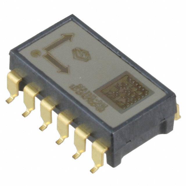
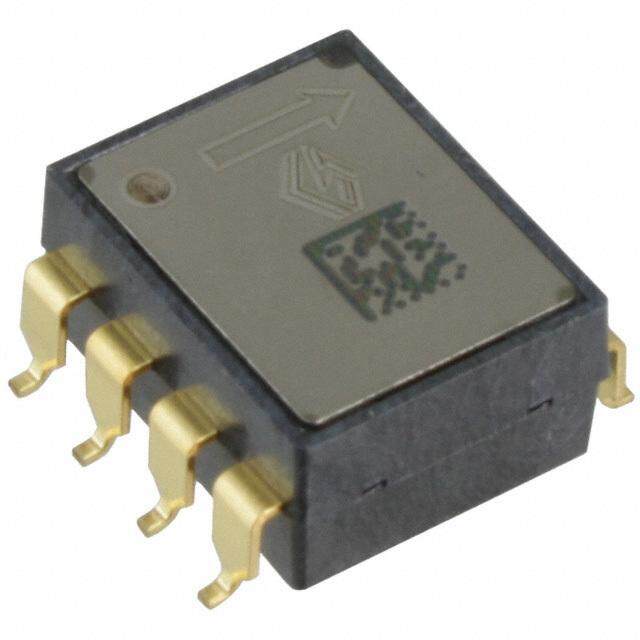
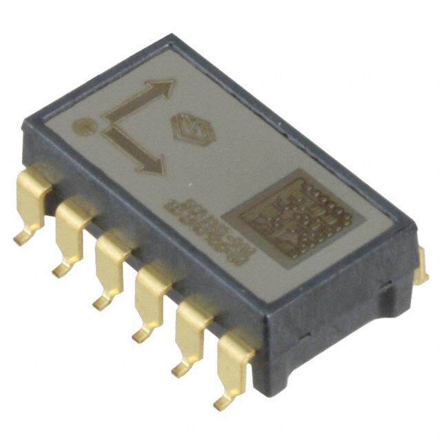
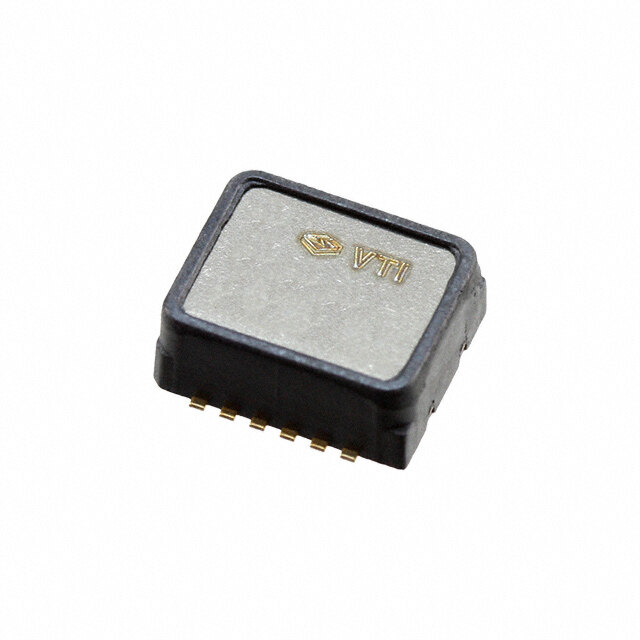
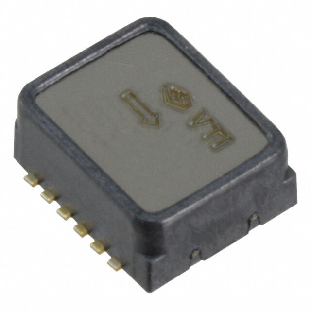
ICGOO电子元器件商城为您提供SCA100T-D01-1由Murata设计生产,在icgoo商城现货销售,并且可以通过原厂、代理商等渠道进行代购。 SCA100T-D01-1价格参考。MurataSCA100T-D01-1封装/规格:运动传感器 - 倾角仪, Sensor Inclinometer ±30° X, Y Axis 8 ~ 28Hz Bandwidth 12-SMD, L-Bend。您可以下载SCA100T-D01-1参考资料、Datasheet数据手册功能说明书,资料中有SCA100T-D01-1 详细功能的应用电路图电压和使用方法及教程。
Murata Electronics North America 的 SCA100T-D01-1 是一款高精度的倾角仪(倾斜传感器),属于运动传感器类别。它广泛应用于需要精确测量角度变化或监测设备姿态的场景。以下是其主要应用场景:

 1. 工业自动化
   - 在工业机器人、机械臂和自动化设备中,用于实时监测设备的姿态和角度,确保操作的精准性。
   - 应用于生产线上的水平校准,确保设备在运行过程中保持稳定。

 2. 建筑与基础设施
   - 用于监测建筑物、桥梁或塔架的倾斜状态,预防结构变形或倒塌。
   - 在施工设备(如起重机、挖掘机)中,帮助操作员保持设备的平衡和稳定性。

 3. 航空航天与航海
   - 在无人机、飞行器或船舶中,作为惯性导航系统的一部分,提供姿态信息以辅助稳定控制。
   - 用于监测飞行器或船只的倾斜角度,优化航行性能并提高安全性。

 4. 医疗设备
   - 在康复设备或步态分析系统中,用于监测患者的姿势和运动轨迹。
   - 用于手术机器人或精密医疗仪器中,确保设备的稳定性和准确性。

 5. 农业与工程机械
   - 在农业机械(如拖拉机、播种机)中,用于监测地形坡度,优化作业效率。
   - 在采矿或土方工程中,帮助设备适应不平整地形,确保安全操作。

 6. 消费电子与物联网
   - 在智能家居设备中,用于检测家具或家电的倾斜状态,防止意外发生。
   - 在运动追踪设备中,记录用户的姿态变化或运动数据。

 7. 能源与石油行业
   - 在钻井平台或管道监测中,用于检测设备的倾斜角度,避免因不稳定导致的安全隐患。
   - 在风力发电机中,帮助调整叶片角度以优化发电效率。

SCA100T-D01-1 具有高精度、低噪声和宽温度范围的特点,能够在严苛环境下可靠工作,因此适用于上述各种复杂场景。
| 参数 | 数值 |
| 产品目录 | |
| 描述 | INCLINOMETER DUAL 0.5G DIL12 SMD测斜计 2-Axis Inclinometer Analog |
| 产品分类 | 倾斜仪运动与定位传感器 |
| 品牌 | Murata Electronics North America |
| 产品手册 | |
| 产品图片 |
|
| rohs | 符合RoHS无铅 / 符合限制有害物质指令(RoHS)规范要求 |
| 产品系列 | 测斜计,Murata Electronics SCA100T-D01-1- |
| 数据手册 | |
| 产品型号 | SCA100T-D01-1 |
| 产品 | Tilt Sensor |
| 产品培训模块 | http://www.digikey.cn/PTM/IndividualPTM.page?site=cn&lang=zhs&ptm=30253 |
| 产品目录页面 | |
| 产品种类 | 测斜计 |
| 其它名称 | 551-1002-1 |
| 商标 | Murata Electronics |
| 安装风格 | SMD/SMT |
| 封装 | Bulk |
| 封装/外壳 | 12-SMD |
| 工作角 | 30 deg |
| 工厂包装数量 | 100 |
| 带宽 | 8 ~ 28Hz |
| 接口 | SPI |
| 标准包装 | 1 |
| 测量范围 | ±30° |
| 灵敏度 | 4V/g |
| 特色产品 | http://www.digikey.cn/product-highlights/zh/mems-sensors/52775 |
| 系列 | SCA100T |
| 轴 | X,Y |
| 输出类型 | 模拟 |
| 额定电压 | 4.75 V ~ 5.25 V |


- 商务部:美国ITC正式对集成电路等产品启动337调查
- 曝三星4nm工艺存在良率问题 高通将骁龙8 Gen1或转产台积电
- 太阳诱电将投资9.5亿元在常州建新厂生产MLCC 预计2023年完工
- 英特尔发布欧洲新工厂建设计划 深化IDM 2.0 战略
- 台积电先进制程称霸业界 有大客户加持明年业绩稳了
- 达到5530亿美元!SIA预计今年全球半导体销售额将创下新高
- 英特尔拟将自动驾驶子公司Mobileye上市 估值或超500亿美元
- 三星加码芯片和SET,合并消费电子和移动部门,撤换高东真等 CEO
- 三星电子宣布重大人事变动 还合并消费电子和移动部门
- 海关总署:前11个月进口集成电路产品价值2.52万亿元 增长14.8%

PDF Datasheet 数据手册内容提取
Product Family Specification SCA100T Series Data Sheet THE SCA100T DUAL AXIS INCLINOMETER SERIES The SCA100T Series is a 3D-MEMS-based dual axis inclinometer family that provides instrumentation grade performance for leveling applications. The measuring axes of the sensing elements are parallel to the mounting plane and orthogonal to each other. Low temperature dependency, high resolution and low noise, together a with robust sensing element design, make the SCA100T the ideal choice for leveling instruments. The Murata inclinometers are unsensitive to vibration, due to their over damped sensing elements, and can withstand mechanical shocks of up to 20000 g. Features Dual axis inclination measurement (X and Y) Digital SPI inclination and temperature output Measuring ranges ±30° SCA100T-D01 and Comprehensive failure detection features ± 90° SCA100T-D02 o True self test by deflecting the sensing 0.0035° resolution (10 Hz BW, analog output) elements’ proof mass by electrostatic force. Sensing element controlled over damped o Continuous sensing element interconnection frequency response (-3dB 18Hz) failure check. Robust design, high shock durability (20000g) o Continuous memory parity check. High stability over temperature and time RoHS compliant Single +5 V supply Compatible with Pb-free reflow solder process Ratiometric analog voltage outputs Applications Platform leveling and stabilization Leveling instruments 360° vertical orientation measurement Construction levels 12 VDD Sensing Signal conditioning 11 OUT_1 element 1 and filtering A/D conversion 10 ST_1 Self test 1 EEPROM Temperature calibration Sensor 1 SCK memory 9 ST_2 Self test 2 3 MISO SPI interface 4 MOSI 7 CSB Sensing Signal conditioning 5 OUT_2 element 2 and filtering 6 GND Figure 1. Functional block diagram Murata Electronics Oy Subject to changes 1/17 www.muratamems.fi Doc.Nr. 8261800 Rev.B2
SCA100T Series TABLE OF CONTENTS The SCA100T Dual Axis Inclinometer Series ......................................................................... 1 Features............................................................................................................................................. 1 Applications ...................................................................................................................................... 1 Table of Contents...................................................................................................................... 2 1 Electrical Specifications ..................................................................................................... 3 1.1 Absolute Maximum Ratings ................................................................................................... 3 1.2 Performance Characteristics .................................................................................................. 3 1.3 Electrical Characteristics ....................................................................................................... 4 1.4 SPI Interface DC Characteristics ............................................................................................ 4 1.5 SPI Interface AC Characteristics ............................................................................................ 4 1.6 SPI Interface Timing Specifications ....................................................................................... 5 1.7 Electrical Connection.............................................................................................................. 6 1.8 Typical Performance Characteristics .................................................................................... 6 1.8.1 Additional External Compensation ...................................................................................... 7 2 Functional Description ....................................................................................................... 9 2.1 Measuring Directions .............................................................................................................. 9 2.2 Voltage to Angle Conversion ................................................................................................. 9 2.3 Ratiometric Output ................................................................................................................ 10 2.4 SPI Serial Interface ................................................................................................................ 10 2.5 Digital Output to Angle Conversion ..................................................................................... 12 2.6 Self Test and Failure Detection Modes ................................................................................ 13 2.7 Temperature Measurement .................................................................................................. 14 3 Application Information .................................................................................................... 15 3.1 Recommended Circuit Diagrams and Printed Circuit Board Layouts ............................... 15 3.2 Recommended Printed Circuit Board Footprint ................................................................. 16 4 Mechanical Specifications and Reflow Soldering .......................................................... 16 4.1 Mechanical Specifications (Reference only) ....................................................................... 16 4.2 Reflow Soldering ................................................................................................................... 17 Murata Electronics Oy Subject to changes 2/17 www.muratamems.fi Doc. nr. 8261800 Rev.B2
SCA100T Series 1 Electrical Specifications The SCA100T product family comprises two versions, the SCA100T-D01 and the SCA100T-D02 that differ in measurement range. The product version specific performance specifications are listed in the table SCA100T performance characteristics below. All other specifications are common with both versions. Vdd=5.00V and ambient temperature unless otherwise specified. 1.1 Absolute Maximum Ratings Supply voltage (VDD) -0.3 V to +5.5V Voltage at input / output pins -0.3V to (VDD + 0.3V) Storage temperature -55°C to +125°C Operating temperature -40°C to +125°C Mechanical shock Drop from 1 meter onto a concrete surface (20000g). Powered or non-powered ESD Protection: -Human Body Model ±2 kV -Charge Device Model ±500 V Cleaning Ultrasonic cleaning not allowed 1.2 Performance Characteristics Parameter Condition SCA100T SCA100T Units -D01 -D02 Measuring range Nominal ±30 ±90 ° ±0.5 ±1.0 g Frequency response –3dB LP (1 8-28 8-28 Hz Offset (Output at 0g) Ratiometric output Vdd/2 Vdd/2 V Offset calibration error ±0.11 ±0.23 ° Offset Digital Output 1024 1024 LSB Sensitivity 4 2 V/g between 0…1° (2 70 35 mV/° Sensitivity calibration ±0.5 ±0.5 % error Sensitivity Digital Output 1638 819 LSB / g Offset temperature -25…85°C (typical) ±0.008 ±0.008 °/°C dependency -40…125°C (max) ±0.86 ±0.86 ° Sensitivity temperature -25...85°C (typical) ±0.014 ±0.014 %/°C dependency -40…125°C (max) -2.5...+1 -2.5...+1 % Typical non-linearity Measuring range ±0.11 ±0.57 ° Digital output resolution 11 11 Bits between 0…1° (2 0.035 0.07 ° / LSB Output noise density From DC...100Hz 0.0008 0.0008 / Hz Analog output resolution(4 Bandwidth 10 Hz(3 0.0035 0.0035 ° Ratiometric error(4 Vdd = 4.75...5.25V ±2 ±2 % Cross-axis sensitivity Max. 4 4 % Note 1. The frequency response is determined by the sensing element’s internal gas damping. Note 2. The angle output has SIN curve relationship to voltage output Note 3. 1st degree low pass filtered output Resolution = Noise density * √(bandwidth*1.6) Note 4. Typical value for most of the components Murata Electronics Oy Subject to changes 3/17 www.muratamems.fi Doc. nr. 8261800 Rev.B2
SCA100T Series 1.3 Electrical Characteristics Parameter Condition Min. Typ Max. Units Supply voltage Vdd 4.75 5.0 5.25 V Current Vdd = 5 V; No load 4 5 mA consumption Operating -40 +125 °C temperature Analog resistive Vout to Vdd or GND 10 kOhm output load Analog capacitive Vout to Vdd or GND 20 nF output load Start-up delay Reset and parity check 10 ms 1.4 SPI Interface DC Characteristics Parameter Conditions Symbol Min Typ Max Unit Input terminal CSB Pull up current V = 0 V I 13 22 35 A IN PU Input high voltage V 4 Vdd+0.3 V IH Input low voltage V -0.3 1 V IL Hysteresis V 0.23*Vdd V HYST Input capacitance C 2 pF IN Input terminal MOSI, SCK Pull down current V = 5 V I 9 17 29 A IN PD Input high voltage V 4 Vdd+0.3 V IH Input low voltage V -0.3 1 V IL Hysteresis V 0.23*Vdd V HYST Input capacitance C 2 pF IN Output terminal MISO Output high voltage I > -1mA V Vdd- V OH 0.5 Output low voltage I < 1 mA V 0.5 V OL Tristate leakage 0 < V < I 5 100 pA MISO LEAK Vdd 1.5 SPI Interface AC Characteristics Parameter Condition Min. Typ. Max. Units Output load @500kHz 1 nF SPI clock frequency 500 kHz Internal A/D conversion time 150 s Data transfer time for 8bit command and @500kHz 38 s 11bit data Murata Electronics Oy Subject to changes 4/17 www.muratamems.fi Doc. nr. 8261800 Rev.B2
SCA100T Series 1.6 SPI Interface Timing Specifications Parameter Conditions Symbol Min. Typ. Max. Unit Terminal CSB, SCK Time from CSB (10%) T 120 ns LS1 to SCK (90%) Time from SCK (10%) T 120 ns LS2 to CSB (90%) Terminal SCK SCK low time Load T 1 s CL capacitance at MISO < 2 nF SCK high time Load T 1 s CH capacitance at MISO < 2 nF Terminal MOSI, SCK Time from changing MOSI T 30 ns SET (10%, 90%) to SCK (90%). Data setup time Time from SCK (90%) to T 30 ns HOL changing MOSI (10%,90%). Data hold time Terminal MISO, CSB Time from CSB (10%) to stable Load T 10 100 ns VAL1 MISO (10%, 90%). capacitance at MISO < 15 pF Time from CSB (90%) to high Load T 10 100 ns LZ impedance state of capacitance at MISO. MISO < 15 pF Terminal MISO, SCK Time from SCK (10%) to stable Load T 100 ns VAL2 MISO (10%, 90%). capacitance at MISO < 15 pF Terminal CSB Time between SPI cycles, CSB at T 15 s LH high level (90%) When using SPI commands TLH 150 s RDAX, RDAY, RWTR: Time between conversion cycles, CSB at high level (90%) T T T T T LS1 CH CL LS2 LH CSB SCK THOL TSET MOSI MSB in DATA in LSB in T T T VAL1 VAL2 LZ MISO MSB out DATA out LSB out Figure 2. Timing diagram for SPI communication Murata Electronics Oy Subject to changes 5/17 www.muratamems.fi Doc. nr. 8261800 Rev.B2
SCA100T Series 1.7 Electrical Connection If the SPI interface is not used SCK (pin1), MISO (pin3), MOSI (pin4) and CSB (pin7) must be left floating. Self-test can be activated applying logic “1” (positive supply voltage level) to ST_1 or ST_2 pins (pins 10 or 9). Self-test must not be activated for both channels at the same time. If ST feature is not used pins 9 and 10 must be left floating or connected to GND. Inclination signals are provided from pins OUT_1 and OUT_2. SSCCKK 1 12 VVDDDD Ext_C_1 2 11 OOUUTT_1_1 MMISIOSO 3 10 STS_T1_/1T est_in MMOOSSI I 4 9 STS_T2_2 OOUUTT__22 5 8 Ex t_C_2 GNVDS S 6 7 CCSBSB Figure 3. SCA100T electrical connection No. Node I/O Description 1 SCK Input Serial clock 2 NC Input No connect, left floating 3 MISO Output Master in slave out; data output 4 MOSI Input Master out slave in; data input 5 Out_2 Output Y axis Output (Ch 2) 6 GND Supply Ground 7 CSB Input Chip select (active low) 8 NC Input No connect, left floating 9 ST_2 Input Self test input for Ch 2 10 ST_1 Input Self test input for Ch 1 11 Out_1 Output X axis Output (Ch 1) 12 VDD Supply Positive supply voltage (+5V DC) 1.8 Typical Performance Characteristics Typical offset and sensitivity temperature dependencies of the SCA100T are presented in following diagrams. These results represent the typical performance of SCA100T components. The mean value and 3 sigma limits (mean ± 3 standard deviation) and specification limits are presented in following diagrams. The 3 sigma limits represents 99.73% of the SCA100T population. Murata Electronics Oy Subject to changes 6/17 www.muratamems.fi Doc. nr. 8261800 Rev.B2
SCA100T Series Temperature dependency of SCA100T offset 1 specification limit 0.8 0.6 es] 0.4 egre 0.2 Average or [d 0 +3 sigma err -0.2 -3 sigma et offs -0.4 -0.6 -0.8 specification limit -1 -40 -20 0 20 40 60 80 100 120 Temp [°C] Figure 4. Typical temperature dependency of SCA100T offset Temperature dependency of SCA100T sensitivity 1.00 specification limit 0.50 %] 0.00 or [ err -0.50 Average y +3 sigma nsitivit -1.00 -3 sigma se -1.50 -2.00 -2.50 specification limit -40 -20 0 20 40 60 80 100 120 Temp [°C] Figure 5. Typical temperature dependency of SCA100T sensitivity 1.8.1 Additional External Compensation To achieve the best possible accuracy, the temperature measurement information and typical temperature dependency curves can be used for SCA100T offset and sensitivity temperature dependency compensation. The equation of fitted 3rd order polynome curve for offset compensation is: Offcorr 0.0000006*T30.0001*T2 0.0039*T 0.0522 Where: Offcorr: 3rd order polynome fitted to average offset temperature dependency curve T temperature in °C (Refer to paragraph 2.7 Temperature Measurement) The calculated compensation curve can be used to compensate the temperature dependency of the SCA100T offset by using following equation: OFFSETcompOffsetOffcorr Where: OFFSETcomp temperature compensated offset in degrees Offset Nominal offset in degrees Murata Electronics Oy Subject to changes 7/17 www.muratamems.fi Doc. nr. 8261800 Rev.B2
SCA100T Series The equation of fitted 2nd order polynome curve for sensitivity compensation is: Scorr 0.00011*T2 0.0022*T 0.0408 Where: Scorr: 2nd order polynome fitted to average sensitivity temperature dependency curve T temperature in °C The calculated compensation curve can be used to compensate the temperature dependency of the SCA100T sensitivity by using following equation: SENScompSENS*(1Scorr/100) Where: SENScomp temperature compensated sensitivity SENS Nominal sensitivity (4V/g SCA100T-D01, 2V/g SCA100T-D02) The typical offset and sensitivity temperature dependency after external compensation is shown in the pictures below. Temperature dependency of externally compensated SCA100T offset 1 0.8 0.6 s] ee 0.4 egr 0.2 Average d or [ 0 +3 sigma err -0.2 -3 sigma set -0.4 off -0.6 -0.8 -1 -40 -20 0 20 40 60 80 100 120 Temp [°C] Figure 6. The temperature dependency of an externally compensated SCA100T offset Temperature dependency of externally compensated SCA100T sensitivity 1 0.8 0.6 error [%] 00..24 Average sitivity -0.20 +-33 ssigigmmaa en -0.4 s -0.6 -0.8 -1 -40 -20 0 20 40 60 80 100 120 Temp [°C] Figure 7. The temperature dependency of an externally compensated SCA100T sensitivity Murata Electronics Oy Subject to changes 8/17 www.muratamems.fi Doc. nr. 8261800 Rev.B2
SCA100T Series 2 Functional Description 2.1 Measuring Directions X-axis Y-axis VOUT > VOUT =2.5V > VOUT Figure 8. The measuring directions of the SCA100T 2.2 Voltage to Angle Conversion Analog output can be transferred to angle using the following equation for conversion: V Offset arcsin out Sensitivity where: Offset = output of the device at 0° inclination position, Sensitivity is the sensitivity of the device and V is the output of the SCA100T. The nominal offset is 2.5 V and the sensitivity is 4 Dout V/g for the SCA100T-D01 and 2 V/g for the SCA100T-D02. Angles close to 0° inclination can be estimated quite accurately with straight line conversion but for the best possible accuracy, arcsine conversion is recommended to be used. The following table shows the angle measurement error if straight line conversion is used. Straight line conversion equation: V Offset out Sensitivity Where: Sensitivity = 70mV/° with SCA100T-D01 or Sensitivity= 35mV/° with SCA100T-D02 Tilt angle [°] Straight line conversion error [°] 0 0 1 0.0027 2 0.0058 3 0.0094 4 0.0140 5 0.0198 10 0.0787 15 0.2185 30 1.668 Murata Electronics Oy Subject to changes 9/17 www.muratamems.fi Doc. nr. 8261800 Rev.B2
SCA100T Series 2.3 Ratiometric Output Ratiometric output means that the zero offset point and sensitivity of the sensor are proportional to the supply voltage. If the SCA100T supply voltage is fluctuating the SCA100T output will also vary. When the same reference voltage for both the SCA100T sensor and the measuring part (A/D- converter) is used, the error caused by reference voltage variation is automatically compensated for. 2.4 SPI Serial Interface A Serial Peripheral Interface (SPI) system consists of one master device and one or more slave devices. The master is defined as a micro controller providing the SPI clock and the slave as any integrated circuit receiving the SPI clock from the master. The ASIC in Murata Electronics’ products always operates as a slave device in master-slave operation mode. The SPI has a 4-wire synchronous serial interface. Data communication is enabled by a low active Slave Select or Chip Select wire (CSB). Data is transmitted by a 3-wire interface consisting of wires for serial data input (MOSI), serial data output (MISO) and serial clock (SCK). MASTER MICROCONTROLLER SLAVE DATA OUT (MOSI) SI DATA IN (MISO) SO SERIAL CLOCK (SCK) SCK SS0 CS SS1 SI SS2 SO SS3 SCK CS SI SO SCK CS SI SO SCK CS Figure 9. Typical SPI connection The SPI interface in Murata products is designed to support any micro controller that uses SPI bus. Communication can be carried out by either a software or hardware based SPI. Please note that in the case of hardware based SPI, the received acceleration data is 11 bits. The data transfer uses the following 4-wire interface: MOSI master out slave in µP → SCA100T MISO master in slave out SCA100T → µP SCK serial clock µP → SCA100T CSB chip select (low active) µP → SCA100T Each transmission starts with a falling edge of CSB and ends with the rising edge. During transmission, commands and data are controlled by SCK and CSB according to the following rules: commands and data are shifted; MSB first, LSB last each output data/status bits are shifted out on the falling edge of SCK (MISO line) Murata Electronics Oy Subject to changes 10/17 www.muratamems.fi Doc. nr. 8261800 Rev.B2
SCA100T Series each bit is sampled on the rising edge of SCK (MOSI line) after the device is selected with the falling edge of CSB, an 8-bit command is received. The command defines the operations to be performed the rising edge of CSB ends all data transfer and resets internal counter and command register if an invalid command is received, no data is shifted into the chip and the MISO remains in high impedance state until the falling edge of CSB. This reinitializes the serial communication. data transfer to MOSI continues immediately after receiving the command in all cases where data is to be written to SCA100T’s internal registers data transfer out from MISO starts with the falling edge of SCK immediately after the last bit of the SPI command is sampled in on the rising edge of SCK maximum SPI clock frequency is 500kHz maximum data transfer speed for RDAX or RDAY is 5300 samples per sec for one channel at 500kHz clock maximum data transfer speed for RDAX and RDAY is 4150 samples per sec for two channel at 500kHz clock SPI command can be either an individual command or a combination of command and data. In the case of combined command and data, the input data follows uninterruptedly the SPI command and the output data is shifted out parallel with the input data. The SPI interface uses an 8-bit instruction (or command) register. The list of commands is given in Table below. Command Command Description: name format MEAS 00000000 Measure mode (normal operation mode after power on) RWTR 00001000 Read temperature data register STX 00001110 Activate Self test for X-channel STY 00001111 Activate Self test for Y-channel RDAX 00010000 Read X-channel acceleration RDAY 00010001 Read Y-channel acceleration Measure mode (MEAS) is standard operation mode after power-up. During normal operation, the MEAS command is the exit command from Self test. Read temperature data register (RWTR) reads temperature data register during normal operation without affecting the operation. The temperature data register is updated every 150 µs. The load operation is disabled whenever the CSB signal is low, hence CSB must stay high at least 150 µs prior to the RWTR command in order to guarantee correct data. The data transfer is presented in Figure 10 below. The data is transferred MSB first. In normal operation, it does not matter what data is written into temperature data register during the RWTR command and hence writing all zeros is recommended. Figure 10. Command and 8 bit temperature data transmission over the SPI Murata Electronics Oy Subject to changes 11/17 www.muratamems.fi Doc. nr. 8261800 Rev.B2
SCA100T Series Self test for X-channel (STX) activates the self test function for the X-channel (Channel 1). The internal charge pump is activated and a high voltage is applied to the X-channel acceleration sensor element electrode. This causes the electrostatic force that deflects the beam of the sensing element and simulates the acceleration to the positive direction. The self-test is de-activated by giving the MEAS command. The self test function must not be activated for both channels at the same time. Self test for Y-channel (STY) activates the self test function for the Y-channel (Channel 2). The internal charge pump is activated and a high voltage is applied to the Y-channel acceleration sensor element electrode. Read X-channel acceleration (RDAX) accesses the AD converted X-channel (Channel 1) acceleration signal stored in acceleration data register X. Read Y-channel acceleration (RDAY) accesses the AD converted Y-channel (Channel 2) acceleration signal stored in acceleration data register Y. During normal operation, acceleration data registers are reloaded every 150 µs. The load operation is disabled whenever the CSB signal is low, hence CSB must stay high at least 150 µs prior the RDAX command in order to guarantee correct data. Data output is an 11-bit digital word that is fed out MSB first and LSB last. Recommended read cycle for X-,Y-channel and temperature: 1. Wait (150 µs) 2. RDAX (38 µs) 3. Wait (15 µs) 4. RDAY (38 µs) 5. Wait (15 µs) 6. RWTR (32 µs) 7. Goto 1. Figure 11. Command and 11 bit acceleration data transmission over the SPI 2.5 Digital Output to Angle Conversion The acceleration measurement results in RDAX and RDAY data registers are in 11 bit digital word format. The data range is from 0 to 2048. The nominal content of RDAX and RDAY data registers in zero angle position are: Binary: 100 0000 0000 Decimal: 1024 The transfer function from differential digital output to angle can be presented as Murata Electronics Oy Subject to changes 12/17 www.muratamems.fi Doc. nr. 8261800 Rev.B2
SCA100T Series D LSB D LSB arcsin out out@0 Sens LSB/g where; D digital output (RDAX or RDAY) out D digital offset value, nominal value = 1024 out@0° angle Sens sensitivity of the device. (SCA100T-D01: 1638, SCA100T-D02: 819) As an example following table contains data register values and calculated differential digital output values with -5, -1 0, 1 and 5 degree tilt angles. Angle Acceleration RDAX (SCA100T- RDAX (SCA100T- [°] [mg] D01) D02) -5 -87.16 dec: 881 dec: 953 bin: 011 0111 0001 bin: 011 1011 1001 -1 -17.45 dec: 995 dec: 1010 bin: 011 1110 0011 bin: 011 1111 0010 0 0 dec: 1024 dec: 1024 bin: 100 0000 0000 bin: 100 0000 0000 1 17.45 dec: 1053 dec: 1038 bin: 100 0001 1101 bin: 100 0000 1110 5 87.16 dec: 1167 dec: 1095 bin: 100 1000 1111 bin: 100 0100 0111 2.6 Self Test and Failure Detection Modes To ensure reliable measurement results the SCA100T has continuous interconnection failure and calibration memory validity detection. A detected failure forces the output signal close to power supply ground or VDD level, outside the normal output range. The calibration memory validity is verified by continuously running parity check for the control register memory content. In the case where a parity error is detected, the control register is automatically re-loaded from the EEPROM. If a new parity error is detected after re-loading data both analog output voltages are forced to go close to ground level (<0.25 V) and SPI outputs go below 102 counts. The SCA100T also includes a separate self test mode. The true self test simulates acceleration, or deceleration, using an electrostatic force. The electrostatic force simulates acceleration that is high enough to deflect the proof mass to the extreme positive position, and this causes the output signal to go to the maximum value. The self test function is activated either by a separate on-off command on the self test input, or through the SPI. To ensure that output goes to positive end product must be in 0g position. For position below 0g output change might be limited to +1g change of the output. The self-test generates an electrostatic force, deflecting the sensing element’s proof mass, thus checking the complete signal path. The true self test performs following checks: Sensing element movement check ASIC signal path check PCB signal path check Micro controller A/D and signal path check The created deflection can be seen in both the SPI and analogue output.s The self test function is activated digitally by a STX or STY command, and de-activated by a MEAS command. Self test can be also activated applying logic”1” (positive supply voltage level) to ST pins (pins 9 & 10) of SCA100T. The self test Input high voltage level is 4 – Vdd+0.3 V and input low voltage level is 0.3 – 1 V. The self test function must not be activated for both channels at the same time. Murata Electronics Oy Subject to changes 13/17 www.muratamems.fi Doc. nr. 8261800 Rev.B2
SCA100T Series 5 V ST pin voltage 0 V 5V V1 V2 V3 Vout T1 T2 T3 0 V T5 T4 Figure 12. Self test wave forms V1 = initial output voltage before the self test function is activated. V2 = output voltage during the self test function. V3 = output voltage after the self test function has been de-activated and after stabilization time Please note that the error band specified for V3 is to guarantee that the output is within 5% of the initial value after the specified stabilization time. After a longer time (max. 1 second) V1=V3. T1 = Pulse length for Self test activation T2 = Saturation delay T3 = Recovery time T4 = Stabilization time =T2+T3 T5 = Rise time during self test. Self test characteristics: T1 [ms] T2 [ms] T3 [ms] T4 [ms] T5 [ms] V2: V3: 20-100 Typ. 25 Typ. 30 Typ. 55 Typ. 15 Min 0.95*VDD 0.95*V1-1.05*V1 (4.75V @Vdd=5V) 2.7 Temperature Measurement The SCA100T has an internal temperature sensor, which is used for internal offset compensation. The temperature information is also available for additional external compensation. The temperature sensor can be accessed via the SPI interface and the temperature reading is an 8-bit word (0…255). The transfer function is expressed with the following formula: Cou nts197 T 1.083 Where: Counts Temperature reading T Temperature in °C The temperature measurement output is not calibrated. The internal temperature compensation routine uses relative results where absolute accuracy is not needed. If the temperature measurement results are used for additional external compensation then one point calibration in the system level is needed to remove the offset. With external one point calibration the accuracy of the temperature measurement is about ±1 °C. Murata Electronics Oy Subject to changes 14/17 www.muratamems.fi Doc. nr. 8261800 Rev.B2
SCA100T Series 3 Application Information 3.1 Recommended Circuit Diagrams and Printed Circuit Board Layouts The SCA100T should be powered from a well regulated 5 V DC power supply. Coupling of digital noise to the power supply line should be minimized. 100nF filtering capacitor between VDD pin 12 and GND plane must be used. If regulator is placed far from component for example other PCB it is recommend adding more capacitance between VDD and GND to ensure current drive capability of the system. For example 470 pF and 1uF capacitor can be used. The SCA100T has a ratiometric output. To get the best performance use the same reference voltage for both the SCA100T and Analog/Digital converter. Use low pass RC filters with 5.11 kΩ and 10nF on the SCA100T outputs to minimize clock noise. Locate the 100nF power supply filtering capacitor close to VDD pin 12. Use as short a trace length as possible. Connect the other end of capacitor directly to the ground plane. Connect the GND pin 6 to underlying ground plane. Use as wide ground and power supply planes as possible. Avoid narrow power supply or GND connection strips on PCB. Figure 13. Analog connection and layout example Figure 14. SPI connection example Murata Electronics Oy Subject to changes 15/17 www.muratamems.fi Doc. nr. 8261800 Rev.B2
SCA100T Series 3.2 Recommended Printed Circuit Board Footprint Figure 15. Recommended PCB footprint 4 Mechanical Specifications and Reflow Soldering 4.1 Mechanical Specifications (Reference only) Lead frame material: Copper Plating: Nickel followed by Gold Solderability: JEDEC standard: JESD22-B102-C RoHS compliance: RoHS compliant lead free component. Co-planarity error 0.1mm max. The part weights <1.2 g Figure 16. Mechanical dimensions of the SCA100T (Dimensions in mm) Murata Electronics Oy Subject to changes 16/17 www.muratamems.fi Doc. nr. 8261800 Rev.B2
SCA100T Series 4.2 Reflow Soldering The SCA100T is suitable for Sn-Pb eutectic and Pb- free soldering process and mounting with normal SMD pick-and-place equipment. Figure 17. Recommended SCA100T body temperature profile during reflow soldering. Ref. IPC/JEDEC J-STD-020B. Profile feature Sn-Pb Eutectic Pb-free Assembly Assembly Average ramp-up rate (T to T ) 3°C/second max. 3°C/second max. L P Preheat - Temperature min (T ) 100°C 150°C smin - Temperature max (T ) 150°C 200°C smax - Time (min to max) (ts) 60-120 seconds 60-180 seconds Tsmax to T, Ramp up rate 3°C/second max Time maintained above: - Temperature (T) 183°C 217°C L - Time (t) 60-150 seconds 60-150 seconds L Peak temperature (T ) 240 +0/-5°C 250 +0/-5°C P Time within 5°C of actual Peak Temperature (T ) 10-30 seconds 20-40 seconds P Ramp-down rate 6°C/second max 6°C/second max Time 25° to Peak temperature 6 minutes max 8 minutes max The Moisture Sensitivity Level of the part is 3 according to the IPC/JEDEC J-STD-020B. The part should be delivered in a dry pack. The manufacturing floor time (out of bag) in the customer’s end is 168 hours. Notes: Preheating time and temperatures according to guidance from solder paste manufacturer. It is important that the part is parallel to the PCB plane and that there is no angular alignment error from intended measuring direction during assembly process. Wave soldering is not recommended. Ultrasonic cleaning is not allowed. The sensing element may be damaged by an ultrasonic cleaning process Murata Electronics Oy Subject to changes 17/17 www.muratamems.fi Doc. nr. 8261800 Rev.B2