ICGOO在线商城 > 集成电路(IC) > 接口 - UART(通用异步接收器/发送器) > SC16C2550BIB48,151

 Datasheet下载
- 型号: SC16C2550BIB48,151
- 制造商: NXP Semiconductors
- 库位|库存: xxxx|xxxx
- 要求:
| 数量阶梯 | 香港交货 | 国内含税 |
| +xxxx | $xxxx | ¥xxxx |
查看当月历史价格
查看今年历史价格
SC16C2550BIB48,151产品简介:
ICGOO电子元器件商城为您提供SC16C2550BIB48,151由NXP Semiconductors设计生产,在icgoo商城现货销售,并且可以通过原厂、代理商等渠道进行代购。 SC16C2550BIB48,151价格参考¥73.59-¥73.59。NXP SemiconductorsSC16C2550BIB48,151封装/规格:接口 - UART(通用异步接收器/发送器), 。您可以下载SC16C2550BIB48,151参考资料、Datasheet数据手册功能说明书,资料中有SC16C2550BIB48,151 详细功能的应用电路图电压和使用方法及教程。
NXP USA Inc.生产的SC16C2550BIB48,151是一款高性能的UART(通用异步接收器/发送器)接口芯片,广泛应用于需要串行通信的设备和系统中。以下是其主要应用场景:

1. 工业自动化:该芯片可用于工业控制器、可编程逻辑控制器(PLC)以及数据采集系统中,实现设备之间的串行数据传输,支持高效的工业通信协议。

2. 嵌入式系统:在嵌入式设备中,SC16C2550BIB48,151常用于微控制器或处理器与外部设备(如传感器、显示器或其他模块)之间的数据交换,提供稳定可靠的UART通信功能。

3. 通信设备:适用于调制解调器、路由器和网关等通信设备中,用于处理串行数据流,支持多种波特率设置以适应不同的通信需求。

4. 医疗设备:在医疗仪器(如监护仪、超声波设备等)中,该芯片能够实现主机与外设之间的高效数据传输,确保实时性和准确性。

5. 消费电子:用于打印机、扫描仪、数码相机等消费类电子产品中,作为主控芯片与外部设备之间的通信桥梁,支持灵活的数据格式配置。

6. 汽车电子:在车载信息系统中,该UART芯片可用于导航系统、娱乐系统与外部设备的连接,提供稳定的串行通信能力。

7. 物联网(IoT)设备:在智能家居、环境监测等物联网应用中,SC16C2550BIB48,151可以作为数据传输的核心组件,支持低功耗和高效率的串行通信。

总之,SC16C2550BIB48,151凭借其强大的功能和灵活性,适合各种需要高速、可靠串行通信的应用场景,尤其在工业、医疗、通信和消费电子领域表现突出。
| 参数 | 数值 |
| 产品目录 | 集成电路 (IC)半导体 |
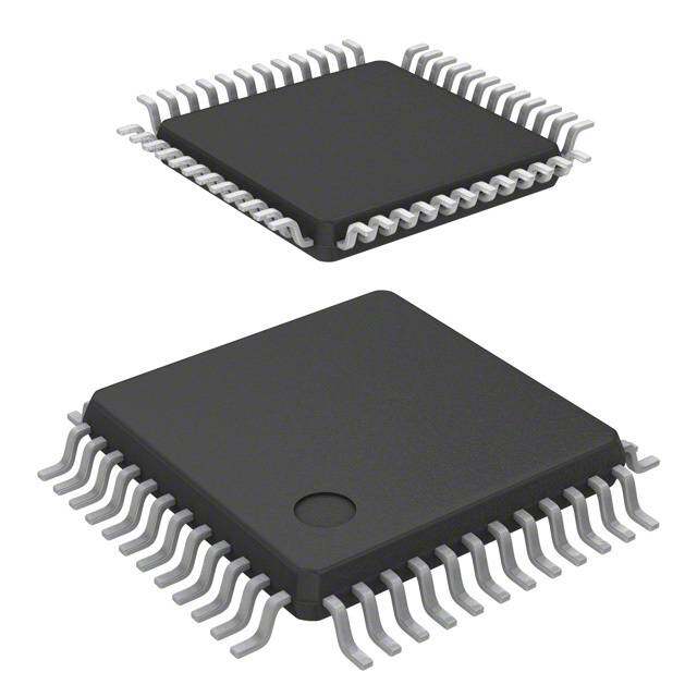
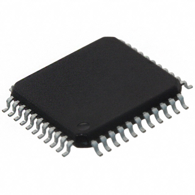
| 描述 | IC UART DUAL W/FIFO 48-LQFPUART 接口集成电路 2CH. UART 16B FIFO |
| 产品分类 | |
| FIFO | 16 字节 |
| 品牌 | NXP Semiconductors |
| 产品手册 | |
| 产品图片 |
|
| rohs | 符合RoHS无铅 / 符合限制有害物质指令(RoHS)规范要求 |
| 产品系列 | 接口 IC,UART 接口集成电路,NXP Semiconductors SC16C2550BIB48,151- |
| 数据手册 | |
| 产品型号 | SC16C2550BIB48,151 |
| PCN封装 | |
| 产品培训模块 | http://www.digikey.cn/PTM/IndividualPTM.page?site=cn&lang=zhs&ptm=11224 |
| 产品目录页面 | |
| 产品种类 | UART 接口集成电路 |
| 供应商器件封装 | 48-LQFP(7x7) |
| 其它名称 | 568-3645 |
| 包装 | 托盘 |
| 协议 | - |
| 商标 | NXP Semiconductors |
| 安装类型 | 表面贴装 |
| 安装风格 | SMD/SMT |
| 封装 | Tray |
| 封装/外壳 | 48-LQFP |
| 封装/箱体 | LQFP-48 |
| 工作电源电压 | 2.5 V, 3.3 V, 5 V |
| 工厂包装数量 | 250 |
| 带CMOS | 是 |
| 带IrDA编码器/解码器 | - |
| 带假起始位检测 | 是 |
| 带并行端口 | - |
| 带自动流量控制 | 是 |
| 带调制解调器控制 | 是 |
| 数据速率 | 5 Mbps |
| 最大工作温度 | + 85 C |
| 最小工作温度 | - 40 C |
| 标准包装 | 250 |
| 特性 | 故障启动位检测 |
| 电压-电源 | 2.5V,3.3V,5V |
| 电源电压-最大 | 5.5 V |
| 电源电压-最小 | 2.25 V |
| 电源电流 | 4.5 mA |
| 类型 | Dual UART with 16-byte FIFOs |
| 通道数 | 2,DUART |
| 通道数量 | 2 Channel |
| 零件号别名 | SC16C2550BIB48-S |


- 商务部:美国ITC正式对集成电路等产品启动337调查
- 曝三星4nm工艺存在良率问题 高通将骁龙8 Gen1或转产台积电
- 太阳诱电将投资9.5亿元在常州建新厂生产MLCC 预计2023年完工
- 英特尔发布欧洲新工厂建设计划 深化IDM 2.0 战略
- 台积电先进制程称霸业界 有大客户加持明年业绩稳了
- 达到5530亿美元!SIA预计今年全球半导体销售额将创下新高
- 英特尔拟将自动驾驶子公司Mobileye上市 估值或超500亿美元
- 三星加码芯片和SET,合并消费电子和移动部门,撤换高东真等 CEO
- 三星电子宣布重大人事变动 还合并消费电子和移动部门
- 海关总署:前11个月进口集成电路产品价值2.52万亿元 增长14.8%


PDF Datasheet 数据手册内容提取
SC16C2550B 5 V, 3.3 V and 2.5 V dual UART, 5 Mbit/s (max.), with 16-byte FIFOs Rev. 05 — 12 January 2009 Product data sheet 1. General description TheSC16C2550B is a two channel Universal Asynchronous Receiver and Transmitter (UART) used for serial data communications. Its principal function is to convert parallel dataintoserialdataandviceversa.TheUARTcanhandleserialdataratesupto5Mbit/s. The SC16C2550B is pin compatible with the ST16C2550. It will power-up to be functionally equivalent to the 16C2450. The SC16C2550B provides enhanced UART functions with 16-byte FIFOs, modem control interface, DMA mode data transfer. The DMA mode data transfer is controlled by the FIFO trigger levels and theTXRDYn and RXRDYn signals. On-board status registers provide the user with error indications and operational status. System interrupts and modem control features may be tailored by software to meet specific user requirements. An internal loopback capability allows on-board diagnostics. Independent programmable baud rate generators are provided to select transmit and receive baud rates. TheSC16C2550B operates at 5V, 3.3V and 2.5V and the industrial temperature range, and is available in plastic PLCC44, LQFP48, DIP40 and HVQFN32 packages. 2. Features n 2 channel UART n 5V, 3.3V and 2.5V operation n 5V tolerant on input only pins1 n Industrial temperature range n Pin and functionally compatible to 16C2450 and software compatible with INS8250, SC16C550 n Up to 5Mbit/s data rate at 5V and 3.3V and 3Mbit/s at 2.5V n 16-byte transmit FIFO to reduce the bandwidth requirement of the external CPU n 16-byte receive FIFO with error flags to reduce the bandwidth requirement of the external CPU n Independent transmit and receive UART control n Four selectable Receive FIFO interrupt trigger levels n Software selectable baud rate generator n Standard asynchronous error and framing bits (Start, Stop and Parity Overrun Break) n Transmit, Receive, Line Status and Data Set interrupts independently controlled 1. For data bus pins D7 to D0, seeTable 23 “Limiting values”.
SC16C2550B NXP Semiconductors 5 V, 3.3 V and 2.5 V dual UART, 5 Mbit/s (max.), with 16-byte FIFOs n Fully programmable character formatting: u 5-bit, 6-bit, 7-bit or 8-bit characters u Even, odd or no-parity formats u 1, 11⁄ or 2-stop bit 2 u Baud generation (DC to 5Mbit/s) n False start-bit detection n Complete status reporting capabilities n 3-state output TTL drive capabilities for bidirectional data bus and control bus n Line break generation and detection n Internal diagnostic capabilities: u Loopback controls for communications link fault isolation n Prioritized interrupt system controls n Modem control functions (CTS,RTS,DSR,DTR,RI,DCD) 3. Ordering information Table 1. Ordering information Type number Package Name Description Version SC16C2550BIA44 PLCC44 plastic leaded chip carrier; 44 leads SOT187-2 SC16C2550BIBS HVQFN32 plastic thermal enhanced very thin quad flat package; no leads; SOT617-1 32terminals; body 5· 5· 0.85mm SC16C2550BIB48 LQFP48 plastic low profile quad flat package; 48 leads; body 7· 7· 1.4mm SOT313-2 SC16C2550BIN40 DIP40 plastic dual in-line package; 40 leads (600mil) SOT129-1 3.1 Ordering options Table 2. Ordering options Type number Topside mark SC16C2550BIA44 SC16C2550BIA44 SC16C2550BIBS 2550B SC16C2550BIB48 16C2550B SC16C2550BIN40 SC16C2550BIN40 SC16C2550B_5 © NXP B.V. 2009. All rights reserved. Product data sheet Rev. 05 — 12 January 2009 2 of 43
SC16C2550B NXP Semiconductors 5 V, 3.3 V and 2.5 V dual UART, 5 Mbit/s (max.), with 16-byte FIFOs 4. Block diagram SC16C2550B TRANSMIT TRANSMIT FIFO SHIFT TXA, TXB REGISTER REGISTER D0 to D7 DATA BUS IOR AND IOW CONTROL RESET LOGIC S E RECEIVE RECEIVE S LIN ALS REGFIIFSOTER RESGHISIFTTER RXA, RXB U N B G T DSI A0 to A2 REGISTER CONNECANONTROL CSA SELECT ER C CSB LOGIC NT I DTRA, DTRB RTSA, RTSB OP2A, OP2B MODEM CONTROL LOGIC CTSA, CTSB INTA, INTB INTERRUPT CLOCK AND RIA, RIB TXRDYA, TXRDYB CONTROL BAUD RATE CDA, CDB RXRDYA, RXRDYB LOGIC GENERATOR DSRA, DSRB 002aaa595 XTAL1 XTAL2 Fig 1. Block diagram of SC16C2550B SC16C2550B_5 © NXP B.V. 2009. All rights reserved. Product data sheet Rev. 05 — 12 January 2009 3 of 43
SC16C2550B NXP Semiconductors 5 V, 3.3 V and 2.5 V dual UART, 5 Mbit/s (max.), with 16-byte FIFOs 5. Pinning information 5.1 Pinning A terminal 1 5 4 3 2 1 0 CC TS index area D D D D D D V C 2 1 0 9 8 7 6 5 3 3 3 2 2 2 2 2 D6 1 24 RESET D7 2 23 RTSA RXB 3 22 OP2A RXA 4 21 INTA SC16C2550BIBS TXA 5 20 INTB TXB 6 19 A0 OP2B 7 18 A1 CSA 8 17 A2 9 10 11 12 13 14 15 16 B 1 2 W D R B B CS TAL TAL IO GN IO RTS CTS 002aab746 X X Transparent top view Fig 2. Pin configuration for HVQFN32 SC16C2550BIN40 D0 1 40 VCC D1 2 39 RIA D2 3 38 CDA D3 4 37 DSRA D4 5 36 CTSA D5 6 35 RESET D6 7 34 DTRB D7 8 33 DTRA RXB 9 32 RTSA RXA 10 31 OP2A TXA 11 30 INTA TXB 12 29 INTB OP2B 13 28 A0 CSA 14 27 A1 CSB 15 26 A2 XTAL1 16 25 CTSB XTAL2 17 24 RTSB IOW 18 23 RIB CDB 19 22 DSRB GND 20 21 IOR 002aaa596 Fig 3. Pin configuration for DIP40 SC16C2550B_5 © NXP B.V. 2009. All rights reserved. Product data sheet Rev. 05 — 12 January 2009 4 of 43
SC16C2550B NXP Semiconductors 5 V, 3.3 V and 2.5 V dual UART, 5 Mbit/s (max.), with 16-byte FIFOs A Y D A A D4 D3 D2 D1 D0 TXR VCC RIA CDA DSR CTS 6 5 4 3 2 1 44 43 42 41 40 D5 7 39 RESET D6 8 38 DTRB D7 9 37 DTRA RXB 10 36 RTSA RXA 11 35 OP2A TXRDYB 12 SC16C2550BIA44 34 RXRDYA TXA 13 33 INTA TXB 14 32 INTB OP2B 15 31 A0 CSA 16 30 A1 CSB 17 29 A2 8 9 0 1 2 3 4 5 6 7 8 1 1 2 2 2 2 2 2 2 2 2 002aaa597 1 2 W B D B R B B B B XTAL XTAL IO CD GN XRDY IO DSR RI RTS CTS R Fig 4. Pin configuration for PLCC44 A Y D A A D4 D3 D2 D1 D0 TXR VCC RIA CDA DSR CTS n.c. 8 7 6 5 4 3 2 1 0 9 8 7 4 4 4 4 4 4 4 4 4 3 3 3 D5 1 36 RESET D6 2 35 DTRB D7 3 34 DTRA RXB 4 33 RTSA RXA 5 32 OP2A TXRDYB 6 31 RXRDYA SC16C2550BIB48 TXA 7 30 INTA TXB 8 29 INTB OP2B 9 28 A0 CSA 10 27 A1 CSB 11 26 A2 n.c. 12 25 n.c. 3 4 5 6 7 8 9 0 1 2 3 4 1 1 1 1 1 1 1 2 2 2 2 2 002aaa598 XTAL1 XTAL2 IOW CDB GND XRDYB IOR DSRB RIB RTSB CTSB n.c. R Fig 5. Pin configuration for LQFP48 SC16C2550B_5 © NXP B.V. 2009. All rights reserved. Product data sheet Rev. 05 — 12 January 2009 5 of 43
SC16C2550B NXP Semiconductors 5 V, 3.3 V and 2.5 V dual UART, 5 Mbit/s (max.), with 16-byte FIFOs 5.2 Pin description Table 3. Pin description Symbol Pin Type Description HVQFN32 DIP40 PLCC44 LQFP48 A0 19 28 31 28 I Address 0 select bit. Internal register address selection. A1 18 27 30 27 I Address 1 select bit. Internal register address selection. A2 17 26 29 26 I Address 2 select bit. Internal register address selection. CSA 8 14 16 10 I Chip Select A, B (activeLOW). This function is associated with individual channels, A through B. These pins enable data CSB 9 15 17 11 I transfers between the user CPU and the SC16C2550B for the channel(s) addressed. Individual UART sections (A, B) are addressed by providing a logic0 on the respectiveCSA,CSB pin. D0 27 1 2 44 I/O Databus(bidirectional).Thesepinsarethe8-bit,3-statedata bus for transferring information to or from the controlling CPU. D1 28 2 3 45 I/O D0 is the least significant bit and the first data bit in a transmit D2 29 3 4 46 I/O or receive serial data stream. D3 30 4 5 47 I/O D4 31 5 6 48 I/O D5 32 6 7 1 I/O D6 1 7 8 2 I/O D7 2 8 9 3 I/O GND 13 20 22 17 I Signal and power ground. INTA 21 30 33 30 O Interrupt A, B (3-state). This function is associated with individual channel interrupts, INTA, INTB. INTA, INTB are INTB 20 29 32 29 O enabled when MCR bit3 is set to a logic1, interrupts are enabled in the Interrupt Enable Register (IER) and is active whenaninterruptconditionexists.Interruptconditionsinclude: receiver errors, available receiver buffer data, transmit buffer empty or when a modem status flag is detected. IOR 14 21 24 19 I Read strobe (activeLOW strobe). A logic 0 transition on this pin will load the contents of an internal register defined by address bits A0toA2 onto the SC16C2550B data bus (D0toD7) for access by external CPU. IOW 12 18 20 15 I Write strobe (activeLOW strobe). A logic0 transition on this pinwilltransferthecontentsofthedatabus(D0toD7)fromthe external CPU to an internal register that is defined by address bits A0toA2. OP2A 22 31 35 32 O Output 2 (user-defined). This function is associated with individual channels, A through B. The state at these pin(s) are OP2B 7 13 15 9 O definedbytheuserandthroughMCRregisterbit3.INTA,INTB are set to the active mode andOP2 to logic0 when MCR[3] is set to a logic1. INTA, INTB are set to the 3-state mode and OP2 to a logic1 when MCR[3] is set to a logic0. SeeTable 18 “Modem Control Register bits description”, bit3 (MCR[3]). Since these bits control both the INTA, INTB operation and OP2outputs,onlyonefunctionshouldbeusedatonetime,INT orOP2. SC16C2550B_5 © NXP B.V. 2009. All rights reserved. Product data sheet Rev. 05 — 12 January 2009 6 of 43
SC16C2550B NXP Semiconductors 5 V, 3.3 V and 2.5 V dual UART, 5 Mbit/s (max.), with 16-byte FIFOs Table 3. Pin description …continued Symbol Pin Type Description HVQFN32 DIP40 PLCC44 LQFP48 RESET 24 35 39 36 I Reset(activeHIGH).Alogic1onthispinwillresettheinternal registers and all the outputs. The UART transmitter output and the receiver input will be disabled during reset time. (See Section 7.10 “SC16C2550B external reset condition” for initialization details.) RXRDYA - - 34 31 O ReceiveReadyA,B(activeLOW).Thisfunctionisassociated with PLCC44 and LQFP48 packages only. This function RXRDYB - - 23 18 O provides the RXFIFO/RHR status for individual receive channels (A-B).RXRDYn is primarily intended for monitoring DMA mode1 transfers for the receive data FIFOs. A logic0 indicatesthereisareceivedatatoread/upload,thatis,receive ready status with one or more RX characters available in the FIFO/RHR. This pin is a logic1 when the FIFO/RHR is empty or when the programmed trigger level has not been reached. This signal can also be used for single mode transfers (DMA mode0). TXRDYA - - 1 43 O Transmit Ready A, B (activeLOW). This function is associated with PLCC44 and LQFP48 packages only. These TXRDYB - - 12 6 O outputsprovidetheTXFIFO/THRstatusforindividualtransmit channels (A, B).TXRDYn is primarily intended for monitoring DMA mode1 transfers for the transmit data FIFOs. An individual channel’sTXRDYA,TXRDYB buffer ready status is indicated by logic0, that is, at least one location is empty and available in the FIFO or THR. This pin goes to a logic1 (DMA mode1) when there are no more empty locations in the FIFO orTHR.Thissignalcanalsobeusedforsinglemodetransfers (DMA mode0). V 26 40 44 42 I Power supply input. CC XTAL1 10 16 18 13 I Crystal or external clock input. Functions as a crystal input or as an external clock input. A crystal can be connected between this pin and XTAL2 to form an internal oscillator circuit.Alternatively,anexternalclockcanbeconnectedtothis pin to provide custom data rates. (SeeSection 6.5 “Programmable baud rate generator”.) SeeFigure6. XTAL2 11 17 19 14 O Outputofthecrystaloscillatororbufferedclock.(Seealso XTAL1.) Crystal oscillator output or buffered clock output. ShouldbeleftopenifanexternalclockisconnectedtoXTAL1. For extended frequency operation, this pin should be tied to V via a 2kW resistor. CC CDA - 38 42 40 I Carrier Detect (activeLOW). These inputs are associated with individual UART channels A through B. A logic0 on this CDB - 19 21 16 I pinindicatesthatacarrierhasbeendetectedbythemodemfor that channel. CTSA 25 36 40 38 I CleartoSend(activeLOW).Theseinputsareassociatedwith individual UART channels, A through B. A logic0 on theCTSn CTSB 16 25 28 23 I pinindicatesthemodemordatasetisreadytoaccepttransmit data from the SC16C2550B. Status can be tested by reading MSR[4]. This pin has no effect on the UART’s transmit or receive operation. SC16C2550B_5 © NXP B.V. 2009. All rights reserved. Product data sheet Rev. 05 — 12 January 2009 7 of 43
SC16C2550B NXP Semiconductors 5 V, 3.3 V and 2.5 V dual UART, 5 Mbit/s (max.), with 16-byte FIFOs Table 3. Pin description …continued Symbol Pin Type Description HVQFN32 DIP40 PLCC44 LQFP48 DSRA - 37 41 39 I Data Set Ready (activeLOW). These inputs are associated with individual UART channels, A through B. Alogic0 on this DSRB - 22 25 20 I pinindicatesthemodemordatasetispowered-onandisready fordataexchangewiththeUART.Thispinhasnoeffectonthe UART’s transmit or receive operation. DTRA - 33 37 34 O Data Terminal Ready (activeLOW). These outputs are associated with individual UART channels, A through B. DTRB - 34 38 35 O Alogic0 on this pin indicates that the SC16C2550B is powered-on and ready. This pin can be controlled via the Modem Control Register. Writing a logic1 to MCR[0] will set theDTRn output to logic0, enabling the modem. This pin will be a logic1 after writing a logic0 to MCR[0] or after a reset. This pin has no effect on the UART’s transmit or receive operation. RIA - 39 43 41 I Ring Indicator (activeLOW). These inputs are associated with individual UART channels, A through B. A logic0 on this RIB - 23 26 21 I pinindicatesthemodemhasreceivedaringingsignalfromthe telephoneline.Alogic1transitiononthisinputpinwillgenerate an interrupt. RTSA 23 32 36 33 O RequesttoSend(activeLOW).Theseoutputsareassociated with individual UART channels, A through B. Alogic0 on the RTSB 15 24 27 22 O RTSn pin indicates the transmitter has data ready and waiting to send. Writing a logic1 in the Modem Control Register MCR[1]willsetthispintoalogic0,indicatingdataisavailable. After a reset this pin will be set to a logic 1. This pin has no effect on the UART’s transmit or receive operation. RXA 4 10 11 5 I ReceivedataA,B.Theseinputsareassociatedwithindividual serial channel data to the SC16C2550B receive input circuits, RXB 3 9 10 4 I A and B. The RXn signal will be a logic1 during reset, idle (no data) or when the transmitter is disabled. During the local Loopback mode, the RXn input pin is disabled and TX data is connected to the UART RX input, internally. TXA 5 11 13 7 O Transmit data A, B. These outputs are associated with individual serial transmit channel data from the SC16C2550B. TXB 6 12 14 8 O The TXn signal will be a logic1 during reset, idle (no data) or when the transmitter is disabled. During the local Loopback mode, the TXn output pin is disabled and TX data is internally connected to the UART RX input. n.c. - - - 12, 24, - not connected 25, 37 SC16C2550B_5 © NXP B.V. 2009. All rights reserved. Product data sheet Rev. 05 — 12 January 2009 8 of 43
SC16C2550B NXP Semiconductors 5 V, 3.3 V and 2.5 V dual UART, 5 Mbit/s (max.), with 16-byte FIFOs 6. Functional description TheSC16C2550B provides serial asynchronous receive data synchronization, parallel-to-serial and serial-to-parallel data conversions for both the transmitter and receiversections.Thesefunctionsarenecessaryforconvertingtheserialdatastreaminto parallel data that is required with digital data systems. Synchronization for the serial data stream is accomplished by adding start and stop bits to the transmit data to form a data character(characterorientatedprotocol).Dataintegrityisinsuredbyattachingaparitybit to the data character. The parity bit is checked by the receiver for any transmission bit errors. The electronic circuitry to provide all these functions is fairly complex, especially whenmanufacturedonasingleintegratedsiliconchip.TheSC16C2550Brepresentssuch an integration with greatly enhanced features. TheSC16C2550B is fabricated with an advanced CMOS process. TheSC16C2550B is an upward solution that provides a dual UART capability with 16bytes of transmit and receive FIFO memory, instead of none in the 16C2450. The SC16C2550B is designed to work with high speed modems and shared network environmentsthatrequirefastdataprocessingtime.Increasedperformanceisrealizedin theSC16C2550BbythetransmitandreceiveFIFOs.Thisallowstheexternalprocessorto handlemorenetworkingtaskswithinagiventime.Forexample,theST16C2450withouta receive FIFO, will require unloading of the RHR in 93microseconds (this example uses a character length of 11bits, including start/stop bits at 115.2kbit/s). This means the external CPU will have to service the receive FIFO less than every 100 microseconds. However, with the 16-byte FIFO in theSC16C2550B, the data buffer will not require unloading/loadingfor1.53ms.Thisincreasestheserviceinterval,givingtheexternalCPU additional time for other applications and reducing the overall UART interrupt servicing time. In addition, the four selectable receive FIFO trigger interrupt levels are uniquely provided for maximum data throughput performance especially when operating in a multi-channelenvironment.TheFIFOmemorygreatlyreducesthebandwidthrequirement of the external controlling CPU, increases performance and reduces power consumption. TheSC16C2550B is capable of operation up to 5Mbit/s with a 80MHz clock. With a crystal or external clock input of 7.3728MHz, the user can select data rates up to 460.8kbit/s. TherichfeaturesetoftheSC16C2550Bisavailablethroughinternalregisters.Selectable receive FIFO trigger levels, selectable TX and RX baud rates and modem interface controls are all standard features. Following a power-on reset or an external reset, the SC16C2550B is software compatible with the previous generation, ST16C2450. 6.1 UART A-B functions The UART provides the user with the capability to bidirectionally transfer information between an external CPU, theSC16C2550B package and an external serial device. A logic0 on chip select pinsCSA and/orCSB allows the user to configure, send data, and/or receive data via UART channels AthroughB. Individual channel select functions are shown inTable4. SC16C2550B_5 © NXP B.V. 2009. All rights reserved. Product data sheet Rev. 05 — 12 January 2009 9 of 43
SC16C2550B NXP Semiconductors 5 V, 3.3 V and 2.5 V dual UART, 5 Mbit/s (max.), with 16-byte FIFOs Table 4. Serial port selection Chip Select Function CSA,CSB=1 none CSA=0 UART channel A CSB=0 UART channel B 6.2 Internal registers TheSC16C2550B provides two sets of internal registers (A and B) consisting of 12registers each for monitoring and controlling the functions of each channel of the UART.TheseregistersareshowninTable5.TheUARTregistersfunctionasdataholding registers (THR/RHR), interrupt status and control registers (IER/ISR), a FIFO Control Register (FCR), line status and control registers (LCR/LSR), modem status and control registers(MCR/MSR),programmabledatarate(clock)controlregisters(DLL/DLM)anda user-accessible Scratchpad Register (SPR). Table 5. Internal registers decoding A2 A1 A0 READ mode WRITE mode General register set (THR/RHR, IER/ISR, MCR/MSR, FCR, LCR/LSR, SPR)[1] 0 0 0 Receive Holding Register Transmit Holding Register 0 0 1 Interrupt Enable Register Interrupt Enable Register 0 1 0 Interrupt Status Register FIFO Control Register 0 1 1 Line Control Register Line Control Register 1 0 0 Modem Control Register Modem Control Register 1 0 1 Line Status Register n/a 1 1 0 Modem Status Register n/a 1 1 1 Scratchpad Register Scratchpad Register Baud rate register set (DLL/DLM)[2] 0 0 0 LSB of Divisor Latch LSB of Divisor Latch 0 0 1 MSB of Divisor Latch MSB of Divisor Latch [1] These registers are accessible only when LCR[7] is a logic0. [2] These registers are accessible only when LCR[7] is a logic1. SC16C2550B_5 © NXP B.V. 2009. All rights reserved. Product data sheet Rev. 05 — 12 January 2009 10 of 43
SC16C2550B NXP Semiconductors 5 V, 3.3 V and 2.5 V dual UART, 5 Mbit/s (max.), with 16-byte FIFOs 6.3 FIFO operation The 16-byte transmit and receive data FIFOs are enabled by the FIFO Control Register (FCR)bit0.TheusercansetthereceivetriggerlevelviaFCRbits7:6,butnotthetransmit trigger level. The receiver FIFO section includes a time-out function to ensure data is delivered to the external CPU. An interrupt is generated whenever the Receive Holding Register (RHR) has not been read following the loading of a character or the receive trigger level has not been reached. Table 6. Flow control mechanism Selected trigger level (characters) INTn pin activation 1 1 4 4 8 8 14 14 6.4 Hardware/software and time-out interrupts The interrupts are enabled by IER[3:0]. Care must be taken when handling these interrupts.Followingareset,ifInterruptEnableRegister(IER)bit1=1,theSC16C2550B will issue a Transmit Holding Register interrupt. This interrupt must be serviced prior to continuing operations. The ISR register provides the current singular highest priority interrupt only. A condition can exist where a higher priority interrupt may mask the lower priority interrupt(s). Only after servicing the higher pending interrupt will the lower priority interrupt(s) be reflected in the status register. Servicing the interrupt without investigating further interrupt conditions can result in data errors. When two interrupt conditions have the same priority, it is important to service these interrupts correctly. Receive Data Ready and Receive Time Out have the same interrupt priority (when enabled by IER[0]). The receiver issues an interrupt after the number of characters have reached the programmed trigger level. In this case, theSC16C2550B FIFOmayholdmorecharactersthantheprogrammedtriggerlevel.Followingtheremoval ofadatabyte,theusershouldre-checkLSR[0]foradditionalcharacters.AReceiveTime Out will not occur if the receive FIFO is empty. The time-out counter is reset at the center of each stop bit received or each time the Receive Holding Register (RHR) is read. The actualtime-outvalueis4charactertime,includingdatainformationlength,startbit,parity bit and the size of stop bit, that is, 1· , 1.5· or 2· bit times. SC16C2550B_5 © NXP B.V. 2009. All rights reserved. Product data sheet Rev. 05 — 12 January 2009 11 of 43
SC16C2550B NXP Semiconductors 5 V, 3.3 V and 2.5 V dual UART, 5 Mbit/s (max.), with 16-byte FIFOs 6.5 Programmable baud rate generator TheSC16C2550B supports high speed modem technologies that have increased input data rates by employing data compression schemes. For example, a 33.6kbit/s modem that employs data compression may require a 115.2kbit/s input data rate. A128.0kbit/s ISDNmodemthatsupportsdatacompressionmayneedaninputdatarateof460.8kbit/s. TheSC16C2550B can support a standard data rate of 921.6kbit/s. A single baud rate generator is provided for the transmitter and receiver, allowing independentTX/RXchannelcontrol.Theprogrammablebaudrategeneratoriscapableof operatingwithafrequencyofupto80MHz.Toobtainmaximumdatarate,itisnecessary tousefullrailswingontheclockinput.TheSC16C2550Bcanbeconfiguredforinternalor external clock operation. For internal clock oscillator operation, an industry standard microprocessor crystal is connected externally between the XTAL1 and XTAL2 pins. Alternatively, an external clock can be connected to the XTAL1 pin to clock the internal baud rate generator for standard or custom rates (seeTable7). The generator divides the input 16· clock by any divisor from 1 to (216- 1). The SC16C2550B divides the basic external clock by 16. The basic 16· clock provides table rates to support standard and custom applications using the same system design. The ratetableisconfiguredviatheDLLandDLMinternalregisterfunctions.Customizedbaud rates can be achieved by selecting the proper divisor values for the MSB and LSB sections of baud rate generator. Programming the baud rate generator registers DLM (MSB) and DLL (LSB) provides a usercapabilityforselectingthedesiredfinalbaudrate.TheexampleinTable7showsthe selectable baud rate table available when using a 1.8432MHz external clock input. XTAL1 XTAL2 XTAL1 XTAL2 1.5 kW X1 X1 1.8432 MHz 1.8432 MHz C1 C2 C1 C2 22 pF 33 pF 22 pF 47 pF 002aaa870 Fig 6. Crystal oscillator connection SC16C2550B_5 © NXP B.V. 2009. All rights reserved. Product data sheet Rev. 05 — 12 January 2009 12 of 43
SC16C2550B NXP Semiconductors 5 V, 3.3 V and 2.5 V dual UART, 5 Mbit/s (max.), with 16-byte FIFOs Table 7. Baud rate generator programming table using a 1.8432MHz clock Output Output Output DLM DLL baudrate 16· clockdivisor 16· clockdivisor programvalue programvalue (bit/s) (decimal) (hexadecimal) (hexadecimal) (hexadecimal) 50 2304 900 09 00 75 1536 600 06 00 110 1047 417 04 17 150 768 300 03 00 300 384 180 01 80 600 192 C0 00 C0 1200 96 60 00 60 2400 48 30 00 30 3600 32 20 00 20 4800 24 18 00 18 7200 16 10 00 10 9600 12 0C 00 0C 19.2k 6 06 00 06 38.4k 3 03 00 03 57.6k 2 02 00 02 115.2k 1 01 00 01 6.6 DMA operation TheSC16C2550B FIFO trigger level provides additional flexibility to the user for block mode operation. LSR[6:5] provide an indication when the transmitter is empty or has an empty location(s). The user can optionally operate the transmit and receive FIFOs in the DMA mode (FCR[3]). When the transmit and receive FIFOs are enabled and the DMA mode is de-activated (DMA Mode0), theSC16C2550B activates the interrupt output pin (INTn) for each data transmit or receive operation. When DMA mode is activated (DMA Mode1), the user takes the advantage of block mode operation by loading or unloading the FIFO in a block sequence determined by the receive trigger level and the transmit FIFO. In this mode, theSC16C2550B sets theTXRDYn (orRXRDYn) output pin when characters in the transmit FIFO is below 16 or the characters in the receive FIFOs are above the receive trigger level. 6.7 Loopback mode The internal loopback capability allows on-board diagnostics. In the Loopback mode, the normal modem interface pins are disconnected and reconfigured for loopback internally (seeFigure7).MCR[3:0]registerbitsareusedforcontrollingloopbackdiagnostictesting. In the Loopback mode, the transmitter output (TX) and the receiver input (RX) are disconnected from their associated interface pins and instead are connected together internally. TheCTS,DSR,CD andRI are disconnected from their normal modem control input pins and instead are connected internally toRTS,DTR, MCR[3] (OP2) and MCR[2] (OP1). Loopback test data is entered into the transmit holding register via the user data businterface,D0throughD7.ThetransmitUARTserializesthedataandpassestheserial data to the receive UART via the internal loopback connection. The receive UART SC16C2550B_5 © NXP B.V. 2009. All rights reserved. Product data sheet Rev. 05 — 12 January 2009 13 of 43
SC16C2550B NXP Semiconductors 5 V, 3.3 V and 2.5 V dual UART, 5 Mbit/s (max.), with 16-byte FIFOs convertstheserialdatabackintoparalleldatathatisthenmadeavailableattheuserdata interface D0throughD7. The user optionally compares the received data to the initial transmitted data for verifying error-free operation of the UART TX/RX circuits. In this mode, the receiver and transmitter interrupts are fully operational. The modem control interrupts are also operational. SC16C2550B TRANSMIT TRANSMIT FIFO SHIFT TXA, TXB REGISTERS REGISTER D0 to D7 DATA BUS IOR AND IOW CONTROL RESET LOGIC MCR[4] = 1 RECEIVE RECEIVE ES FIFO SHIFT RXA, RXB N REGISTERS REGISTER S LI ALS U N B G T DSI CSAA0 ,t oC SAB2 RSEEGLISETCETR CONNECANONTROL LOGIC ER C T N I RTSA, RTSB CTSA, CTSB DTRA, DTRB MODEM DSRA, DSRB CONTROL LOGIC (OP1A, OP1B) INTA, INTB INTERRUPT CLOCK AND TXRDYA, TXRDYB CONTROL BAUD RATE RXRDYA, RXRDYB LOGIC GENERATOR RIA, RIB (OP2A, OP2B) CDA, CDB 002aaa599 XTAL1 XTAL2 Fig 7. Internal Loopback mode diagram SC16C2550B_5 © NXP B.V. 2009. All rights reserved. Product data sheet Rev. 05 — 12 January 2009 14 of 43
SC16C2550B NXP Semiconductors 5 V, 3.3 V and 2.5 V dual UART, 5 Mbit/s (max.), with 16-byte FIFOs 7. Register descriptions Table8 details the assigned bit functions for theSC16C2550B internal registers. The assigned bit functions are more fully defined inSection7.1 throughSection7.10. Table 8. SC16C2550B internal registers A2 A1 A0 Register Default[1] Bit 7 Bit 6 Bit 5 Bit 4 Bit 3 Bit 2 Bit 1 Bit 0 General register set[2] 0 0 0 RHR XX bit 7 bit 6 bit 5 bit 4 bit 3 bit 2 bit 1 bit 0 0 0 0 THR XX bit 7 bit 6 bit 5 bit 4 bit 3 bit 2 bit 1 bit 0 0 0 1 IER 00 0 0 0 0 modem receive transmit receive status line holding holding interrupt status register register interrupt interrupt 0 1 0 FCR 00 RCVR RCVR reserved reserved DMA XMIT RCVR FIFOs trigger trigger 0 0 mode FIFO FIFO enable (MSB) (LSB) select reset reset 0 1 0 ISR 01 FIFOs FIFOs 0 0 INT INT INT INT enabled enabled priority priority priority status bit2 bit1 bit0 0 1 1 LCR 00 divisor set break set parity even parity stop bits word word latch parity enable length length enable bit1 bit0 1 0 0 MCR 00 0 0 0 loop OP2/INT (OP1) RTS DTR back enable 1 0 1 LSR 60 FIFO THRand THR break framing parity overrun receive data TSR empty interrupt error error error data error empty ready 1 1 0 MSR X0 CD RI DSR CTS D CD D RI D DSR D CTS 1 1 1 SPR FF bit 7 bit 6 bit 5 bit 4 bit 3 bit 2 bit 1 bit 0 Special register set[3] 0 0 0 DLL XX bit 7 bit 6 bit 5 bit 4 bit 3 bit 2 bit 1 bit 0 0 0 1 DLM XX bit 15 bit 14 bit 13 bit 12 bit 11 bit 10 bit 9 bit 8 [1] The value shown represents the register’s initialized hexadecimal value; X=not applicable. [2] Accessible only when LCR[7] is logic0. [3] Baud rate registers accessible only when LCR[7] is logic1. 7.1 Transmit Holding Register (THR) and Receive Holding Register (RHR) The serial transmitter section consists of an 8-bit Transmit Hold Register (THR) and Transmit Shift Register (TSR). The status of the THR is provided in the Line Status Register(LSR).WritingtotheTHRtransfersthecontentsofthedatabus(D7throughD0) to the TSR and UART via the THR, providing that the THR is empty. The THR empty flag in the LSR register will be set to a logic1 when the transmitter is empty or when data is transferred to the TSR. Note that a write operation can be performed when the THR empty flag is set (logic0=at least one byte in FIFO/THR, logic1=FIFO/THR empty). The serial receive section also contains an 8-bit Receive Holding Register (RHR) and a ReceiveSerialShiftRegister(RSR).ReceivedataisremovedfromtheSC16C2550Band receive FIFO by reading the RHR register. The receive section provides a mechanism to SC16C2550B_5 © NXP B.V. 2009. All rights reserved. Product data sheet Rev. 05 — 12 January 2009 15 of 43
SC16C2550B NXP Semiconductors 5 V, 3.3 V and 2.5 V dual UART, 5 Mbit/s (max.), with 16-byte FIFOs prevent false starts. On the falling edge of a start or false start bit, an internal receiver counter starts counting clocks at the 16· clock rate. After 71⁄ clocks, the start bit time 2 should be shifted to the center of the start bit. At this time the start bit is sampled and if it is still a logic0 it is validated. Evaluating the start bit in this manner prevents the receiver from assembling a false character. Receiver status codes will be posted in the LSR. 7.2 Interrupt Enable Register (IER) The Interrupt Enable Register (IER) masks the interrupts from receiver ready, transmitter empty, line status and modem status registers. These interrupts would normally be seen on the INTA, INTB output pins. Table 9. Interrupt Enable Register bits description Bit Symbol Description 7:4 IER[7:4] not used 3 IER[3] Modem Status Interrupt. This interrupt will be issued whenever there is a modem status change as reflected in MSR[3:0]. logic0 = disable the Modem Status Register interrupt (normal default condition) logic1 = enable the Modem Status Register interrupt 2 IER[2] Receive Line Status interrupt. This interrupt will be issued whenever a receive data error condition exists as reflected in LSR[4:1]. logic0=disablethereceiverlinestatusinterrupt(normaldefaultcondition) logic1 = enable the receiver line status interrupt 1 IER[1] Transmit Holding Register interrupt. In the 16C450 mode, this interrupt will be issued whenever the THR is empty and is associated with LSR[5]. In the FIFO modes, this interrupt will be issued whenever the FIFO is empty. logic0 = disable the Transmit Holding Register Empty (TXRDY) interrupt (normal default condition) logic1 = enable the TXRDY (ISR level 3) interrupt 0 IER[0] Receive Holding Register. In the 16C450 mode, this interrupt will be issued when the RHR has data or is cleared when the RHR is empty. In the FIFO mode, this interrupt will be issued when the FIFO has reached the programmed trigger level or is cleared when the FIFO drops below the trigger level. logic0=disablethereceiverready(ISRlevel2,RXRDY)interrupt(normal default condition) logic1 = enable the RXRDY (ISR level 2) interrupt SC16C2550B_5 © NXP B.V. 2009. All rights reserved. Product data sheet Rev. 05 — 12 January 2009 16 of 43
SC16C2550B NXP Semiconductors 5 V, 3.3 V and 2.5 V dual UART, 5 Mbit/s (max.), with 16-byte FIFOs 7.2.1 IER versus Transmit/Receive FIFO interrupt mode operation When the receive FIFO (FCR[0]=logic1) and receive interrupts (IER[0]=logic1) are enabled, the receive interrupts and register status will reflect the following: • The receive RXRDY interrupt (Level 2 ISR interrupt) is issued to the external CPU when the receive FIFO has reached the programmed trigger level. It will be cleared when the receive FIFO drops below the programmed trigger level. • Receive FIFO status will also be reflected in the user accessible ISR register when the receive FIFO trigger level is reached. Both the ISR register receive status bit and the interrupt will be cleared when the FIFO drops below the trigger level. • The receive data ready bit (LSR[0]) is set as soon as a character is transferred from the shift register (RSR) to the receive FIFO. It is reset when the FIFO is empty. • When the Transmit FIFO and interrupts are enabled, an interrupt is generated when thetransmitFIFOisemptyduetotheunloadingofthedatabytheTSRandUARTfor transmissionviathetransmissionmedia.Theinterruptisclearedeitherbyreadingthe ISR register or by loading the THR with new data characters. 7.2.2 IER versus Receive/Transmit FIFO polled mode operation When FCR[0]=logic1, resetting IER[3:0] enables theSC16C2550B in the FIFO polled mode of operation. In this mode, interrupts are not generated and the user must poll the LSR register for TX and/or RX data status. Since the receiver and transmitter have separate bits in the LSR either or both can be used in the polled mode by selecting respective transmit or receive control bit(s). • LSR[0] will be a logic1 as long as there is one byte in the receive FIFO. • LSR[4:1] will provide the type of receive errors or a receive break, if encountered. • LSR[5] will indicate when the transmit FIFO is empty. • LSR[6]willindicatewhenboththetransmitFIFOandtransmitshiftregisterareempty. • LSR[7] will show if any FIFO data errors occurred. 7.3 FIFO Control Register (FCR) This register is used to enable the FIFOs, clear the FIFOs, set the receive FIFO trigger levels and select the DMA mode. 7.3.1 DMA mode 7.3.1.1 Mode 0 (FCR bit 3 = 0) Set and enable the interrupt for each single transmit or receive operation and is similar to the 16C450 mode. Transmit Ready (TXRDYn) on PLCC44 and LQFP48 packages will go to a logic0 whenever the FIFO (THR, if FIFO is not enabled) is empty. Receive Ready (RXRDYn) on PLCC44 and LQFP48 packages will go to a logic0 whenever the Receive Holding Register (RHR) is loaded with a character. 7.3.1.2 Mode 1 (FCR bit 3 = 1) Setandenabletheinterruptinablockmodeoperation.Thetransmitinterruptissetwhen thetransmitFIFOisempty.TXRDYnonPLCC44andLQFP48packagesremainsalogic0 as long as one empty FIFO location is available. The receive interrupt is set when the receive FIFO fills to the programmed trigger level. However, the FIFO continues to fill SC16C2550B_5 © NXP B.V. 2009. All rights reserved. Product data sheet Rev. 05 — 12 January 2009 17 of 43
SC16C2550B NXP Semiconductors 5 V, 3.3 V and 2.5 V dual UART, 5 Mbit/s (max.), with 16-byte FIFOs regardless of the programmed level until the FIFO is full.RXRDY on PLCC44 and LQFP48 packages transitions LOW when the FIFO reaches the trigger level and transitions HIGH when the FIFO empties. 7.3.2 FIFO mode Table 10. FIFO Control Register bits description Bit Symbol Description 7:6 FCR[7:6] RCVR trigger. These bits are used to set the trigger level for the receive FIFO interrupt. logic0 (or cleared) = normal default condition logic1 = RX trigger level An interrupt is generated when the number of characters in the FIFO equalstheprogrammedtriggerlevel.However,theFIFOwillcontinuetobe loaded until it is full. Refer toTable11. 5:4 FCR[5:4] Not used; initialized to logic0. 3 FCR[3] DMA mode select. logic0 = set DMA mode ‘0’ logic1 = set DMA mode ‘1’ Transmit operation in mode ‘0’: When the SC16C2550B is in the 16C450 mode (FIFOs disabled; FCR[0] = logic0) or in the FIFO mode (FIFOsenabled;FCR[0]=logic1;FCR[3]=logic0)andwhenthereareno charactersinthetransmitFIFOorTransmitHoldingRegister,theTXRDYn pin in PLCC44 or LQFP48 packages will be a logic0. Once active, the TXRDYn pin will go to a logic1 after the first character is loaded into the Transmit Holding Register. Receive operation in mode ‘0’: When the SC16C2550B is in mode‘0’ (FCR[0] = logic0) or in the FIFO mode (FCR[3] = logic0) and there is at least one character in the receive FIFO, theRXRDYn pin will be a logic0. Once active, theRXRDYn pin on PLCC44 and LQFP48 packages will go to a logic1 when there are no more characters in the receiver. Transmit operation in mode ‘1’: When the SC16C2550B is in FIFO mode (FCR[0] = logic1; FCR[3]=logic1), theTXRDYn pin on PLCC44 and LQFP48 packages will be a logic1 when the transmit FIFO is completely full. It will be a logic0 if one or more FIFO locations are empty. Receiveoperationinmode‘1’:WhentheSC16C2550BisinFIFOmode (FCR[0]=logic1;FCR[3]=logic1)andthetriggerlevelhasbeenreached or a Receive Time-out has occurred, theRXRDYn pin on PLCC44 and LQFP48packageswillgotoalogic0.Onceactivated,itwillgotoalogic1 after there are no more characters in the FIFO. 2 FCR[2] XMIT FIFO reset. logic0 = Transmit FIFO not reset (normal default condition). logic1 = clears the contents of the transmit FIFO and resets the FIFO counter logic (the Transmit Shift Register is not cleared or altered). This bit will return to a logic0 after clearing the FIFO. SC16C2550B_5 © NXP B.V. 2009. All rights reserved. Product data sheet Rev. 05 — 12 January 2009 18 of 43
SC16C2550B NXP Semiconductors 5 V, 3.3 V and 2.5 V dual UART, 5 Mbit/s (max.), with 16-byte FIFOs Table 10. FIFO Control Register bits description …continued Bit Symbol Description 1 FCR[1] RCVR FIFO reset. logic0 = Receive FIFO not reset (normal default condition) logic1 = clears the contents of the receive FIFO and resets the FIFO counter logic (the Receive Shift Register is not cleared or altered). This bit will return to a logic0 after clearing the FIFO. 0 FCR[0] FIFOs enabled. logic0 = disable the transmit and receive FIFO (normal default condition) logic1 = enable the transmit and receive FIFO.This bit must be a ‘1’ when other FCR bits are written to or they will not be programmed. Table 11. RCVR trigger levels FCR[7] FCR[6] RX FIFO trigger level 0 0 01 0 1 04 1 0 08 1 1 14 7.4 Interrupt Status Register (ISR) TheSC16C2550B provides four levels of prioritized interrupts to minimize external software interaction. The Interrupt Status Register (ISR) provides the user with four interrupt status bits. Performing a read cycle on the ISR will provide the user with the highest pending interrupt level to be serviced. No other interrupts are acknowledged until the pending interrupt is serviced. A lower level interrupt may be seen after servicing the higher level interrupt and re-reading the interrupt status bits.Table 12 “Interrupt source” shows the data values (bits 3:0) for the four prioritized interrupt levels and the interrupt sources associated with each of these interrupt levels. Table 12. Interrupt source Priority ISR[3] ISR[2] ISR[1] ISR[0] Source of the interrupt level 1 0 1 1 0 LSR (Receiver Line Status Register) 2 0 1 0 0 RXRDY (Received Data Ready) 2 1 1 0 0 RXRDY (Receive Data Time-out) 3 0 0 1 0 TXRDY (Transmitter Holding Register empty) 4 0 0 0 0 MSR (Modem Status Register) SC16C2550B_5 © NXP B.V. 2009. All rights reserved. Product data sheet Rev. 05 — 12 January 2009 19 of 43
SC16C2550B NXP Semiconductors 5 V, 3.3 V and 2.5 V dual UART, 5 Mbit/s (max.), with 16-byte FIFOs Table 13. Interrupt Status Register bits description Bit Symbol Description 7:6 ISR[7:6] FIFOs enabled. These bits are set to a logic0 when the FIFOs are not being used in the 16C450 mode. They are set to a logic1 when the FIFOs are enabled in the SC16C2550B mode. logic0 or cleared = default condition 5:4 ISR[5:4] not used 3:1 ISR[3:1] INTprioritybits2:0.Thesebitsindicatethesourceforapendinginterrupt at interrupt priority levels 1, 2 and 3 (seeTable12). logic0 or cleared = default condition 0 ISR[0] INT status. logic0=aninterruptispendingandtheISRcontentsmaybeusedas a pointer to the appropriate interrupt service routine logic1 = no interrupt pending (normal default condition) 7.5 Line Control Register (LCR) The Line Control Register is used to specify the asynchronous data communication format.Thewordlength,thenumberofstopbitsandtheparityareselectedbywritingthe appropriate bits in this register. Table 14. Line Control Register bits description Bit Symbol Description 7 LCR[7] Divisor latch enable. The internal baud rate counter latch and Enhanced Feature mode enable. logic0= divisor latch disabled (normal default condition) logic1 = divisor latch enabled 6 LCR[6] Setbreak.Whenenabled,theBreakcontrolbitcausesabreakcondition to be transmitted (the TX output is forced to a logic0 state). This condition exists until disabled by setting LCR[6] to a logic0. logic0 = no TX break condition (normal default condition) logic1 = forces the transmitter output (TX) to a logic0 for alerting the remote receiver to a line break condition 5:3 LCR[5:3] Programs the parity conditions (seeTable15) 2 LCR[2] Stop bits. The length of stop bit is specified by this bit in conjunction with the programmed word length (seeTable16). logic0 or cleared = default condition 1:0 LCR[1:0] Word length bits 1, 0. These two bits specify the word length to be transmitted or received (seeTable17). logic0 or cleared = default condition Table 15. LCR[5:3] parity selection LCR[5] LCR[4] LCR[3] Parity selection X X 0 no parity X 0 1 odd parity 0 1 1 even parity 0 0 1 forced parity ‘1’ 1 1 1 forced parity ‘0’ SC16C2550B_5 © NXP B.V. 2009. All rights reserved. Product data sheet Rev. 05 — 12 January 2009 20 of 43
SC16C2550B NXP Semiconductors 5 V, 3.3 V and 2.5 V dual UART, 5 Mbit/s (max.), with 16-byte FIFOs Table 16. LCR[2] stop bit length LCR[2] Word length (bits) Stop bit length (bit times) 0 5, 6, 7, 8 1 1 5 11⁄ 2 1 6, 7, 8 2 Table 17. LCR[1:0] word length LCR[1] LCR[0] Word length (bits) 0 0 5 0 1 6 1 0 7 1 1 8 7.6 Modem Control Register (MCR) This register controls the interface with the modem or a peripheral device. Table 18. Modem Control Register bits description Bit Symbol Description 7:5 MCR[7:5] reserved; set to ‘0’ 4 MCR[4] Loopback.EnablethelocalLoopbackmode(diagnostics).Inthismodethe transmitteroutput(TX)andthereceiverinput(RX),CTS,DSR,CDandRI are disconnected from the SC16C2550B I/O pins. Internally the modem data and control pins are connected into a loopback data configuration (seeFigure7).Inthismode,thereceiverandtransmitterinterruptsremain fully operational. The Modem Control Interrupts are also operational, but the interrupts’ sources are switched to the lower four bits of the Modem Control. Interrupts continue to be controlled by the IER register. logic0 = disable Loopback mode (normal default condition) logic1 = enable local Loopback mode (diagnostics) 3 MCR[3] OP2/INT enable logic0=forcesINT(A,B)outputstothe3-statemodeandsetsOP2toa logic1 (normal default condition) logic1=forcestheINT(A,BoutputstotheactivemodeandsetsOP2to a logic0 2 MCR[2] (OP1).OP1A/OP1B are not available as an external signal in the SC16C2550B. This bit is instead used in the Loopback mode only. In the Loopback mode, this bit is used to write the state of the modemRI interface signal. 1 MCR[1] RTS logic0= forceRTS output to a logic1 (normal default condition) logic1=forceRTS output to a logic0 0 MCR[0] DTR logic0= forceDTR output to a logic1 (normal default condition) logic1 = forceDTR output to a logic0 SC16C2550B_5 © NXP B.V. 2009. All rights reserved. Product data sheet Rev. 05 — 12 January 2009 21 of 43
SC16C2550B NXP Semiconductors 5 V, 3.3 V and 2.5 V dual UART, 5 Mbit/s (max.), with 16-byte FIFOs 7.7 Line Status Register (LSR) This register provides the status of data transfers between theSC16C2550B and theCPU. Table 19. Line Status Register bits description Bit Symbol Description 7 LSR[7] FIFO data error. logic0 = no error (normal default condition) logic1 = at least one parity error, framing error or break indication is in the current FIFO data. This bit is cleared when there are no remaining error flags associated with the remaining data in the FIFO. 6 LSR[6] THR and TSR empty. This bit is the Transmit Empty indicator. This bit is set to a logic1 whenever the Transmit Holding Register and the Transmit Shift Register are both empty. It is reset to logic0 whenever either the THR or TSR contains a data character. In the FIFO mode, this bit is set to ‘1’ whenever the Transmit FIFO and Transmit Shift Register are both empty. 5 LSR[5] THR empty. This bit is the Transmit Holding Register Empty indicator. This bit indicates that the UART is ready to accept a new character for transmission. In addition, this bit causes the UART to issue an interrupt to CPU when the THR interrupt enable is set. The THR bit is set to a logic1 when a character is transferred from the transmit holding register into the transmitter shift register. The bit is reset to a logic0 concurrently with the loading of the transmitter holding register by the CPU. In the FIFO mode, this bit is set when the transmit FIFO is empty; it is cleared when at least 1byte is written to the transmit FIFO. 4 LSR[4] Break interrupt. logic0 = no break condition (normal default condition) logic1 = the receiver received a break signal (RX was a logic0 for one character frame time). In the FIFO mode, only one break character is loaded into the FIFO. 3 LSR[3] Framing error. logic0 = no framing error (normal default condition) logic1=framingerror.Thereceivecharacterdidnothaveavalidstopbit(s).In the FIFO mode, this error is associated with the character at the top of the FIFO. 2 LSR[2] Parity error. logic0 = no parity error (normal default condition logic1 = parity error. The receive character does not have correct parity informationandissuspect.IntheFIFOmode,thiserrorisassociatedwiththe character at the top of the FIFO. 1 LSR[1] Overrun error. logic0= no overrun error (normal default condition) logic1=overrun error. A data overrun error occurred in the Receive Shift Register. This happens when additional data arrives while the FIFO is full. In thiscase,thepreviousdataintheshiftregisterisoverwritten.Notethatunder thiscondition,thedatabyteintheReceiveShiftRegisterisnottransferredinto the FIFO, therefore the data in the FIFO is not corrupted by the error. SC16C2550B_5 © NXP B.V. 2009. All rights reserved. Product data sheet Rev. 05 — 12 January 2009 22 of 43
SC16C2550B NXP Semiconductors 5 V, 3.3 V and 2.5 V dual UART, 5 Mbit/s (max.), with 16-byte FIFOs Table 19. Line Status Register bits description …continued Bit Symbol Description 0 LSR[0] Receive data ready. logic0= no data in Receive Holding Register or FIFO (normal default condition) logic1=datahasbeenreceivedandissavedintheReceiveHoldingRegister or FIFO 7.8 Modem Status Register (MSR) Thisregisterprovidesthecurrentstateofthecontrolinterfacesignalsfromthemodemor other peripheral device to which theSC16C2550B is connected. Four bits of this register are used to indicate the changed information. These bits are set to a logic1 whenever a controlinputfromthemodemchangesstate.Thesebitsaresettoalogic0wheneverthe CPU reads this register. Table 20. Modem Status Register bits description Bit Symbol Description 7 MSR[7] CD. During normal operation, this bit is the complement of theCD input. Reading this bit in the Loopback mode produces the state of MCR[3] (OP2). 6 MSR[6] RI. During normal operation, this bit is the complement of theRI input. Reading this bit in the Loopback mode produces the state of MCR[2] (OP1). 5 MSR[5] DSR. During normal operation, this bit is the complement of theDSR input. During the Loopback mode, this bit is equivalent to MCR[0] (DTR). 4 MSR[4] CTS. During normal operation, this bit is the complement of theCTS input. During the Loopback mode, this bit is equivalent to MCR[1] (RTS). 3 MSR[3] D CD[1] logic 0= noCD change (normal default condition) logic 1=theCD input to the SC16C2550B has changed state since the last time it was read. A modem Status Interrupt will be generated. 2 MSR[2] D RI[1] logic 0= noRI change (normal default condition) logic1=theRIinputtotheSC16C2550Bhaschangedfromalogic0toa logic1. A modem Status Interrupt will be generated. 1 MSR[1] D DSR[1] logic0= noDSR change (normal default condition) logic1=theDSR input to the SC16C2550B has changed state since the last time it was read. A modem Status Interrupt will be generated. 0 MSR[0] D CTS[1] logic0= noCTS change (normal default condition) logic1 = theCTS input to the SC16C2550B has changed state since the last time it was read. A modem Status Interrupt will be generated. [1] Whenever any MSR bit 3:0 is set to logic 1, a Modem Status Interrupt will be generated. SC16C2550B_5 © NXP B.V. 2009. All rights reserved. Product data sheet Rev. 05 — 12 January 2009 23 of 43
SC16C2550B NXP Semiconductors 5 V, 3.3 V and 2.5 V dual UART, 5 Mbit/s (max.), with 16-byte FIFOs 7.9 Scratchpad Register (SPR) TheSC16C2550B provides a temporary data register to store 8bits of user information. 7.10 SC16C2550B external reset condition Table 21. Reset state for registers Register Reset state IER IER[7:0] = 0 FCR FCR[7:0] = 0 ISR ISR[7:1] = 0; ISR[0] = 1 LCR LCR[7:0] = 0 MCR MCR[7:0] = 0 LSR LSR[7] = 0; LSR[6:5] = 1; LSR[4:0] = 0 MSR MSR[7:4] = input signals; MSR[3:0] = 0 SPR SFR[7:0] = 1 DLL DLL[7:0] = X DLM DLM[7:0] = X Table 22. Reset state for outputs Output Reset state TXA, TXB logic 1 OP2A,OP2B logic 1 RTSA,RTSB logic 1 DTRA,DTRB logic 1 INTA, INTB 3-state condition SC16C2550B_5 © NXP B.V. 2009. All rights reserved. Product data sheet Rev. 05 — 12 January 2009 24 of 43
SC16C2550B NXP Semiconductors 5 V, 3.3 V and 2.5 V dual UART, 5 Mbit/s (max.), with 16-byte FIFOs 8. Limiting values Table 23. Limiting values In accordance with the Absolute Maximum Rating System (IEC 60134). Symbol Parameter Conditions Min Max Unit V supply voltage - 7 V CC V voltage on any other pin at D7 to D0 pins GND- 0.3 V +0.3 V n CC at input only pins GND- 0.3 5.3 V T operating temperature - 40 +85 (cid:176) C amb T storage temperature - 65 +150 (cid:176) C stg P /pack total power dissipation per package - 500 mW tot 9. Static characteristics Table 24. Static characteristics T =- 40(cid:176) C to +85(cid:176) C; tolerance of V – 10%; unless otherwise specified. amb CC Symbol Parameter Conditions V =2.5V V =3.3V V =5.0V Unit CC CC CC Min Max Min Max Min Max V clock LOW-level input voltage - 0.3 +0.45 - 0.3 +0.6 - 0.5 +0.6 V IL(clk) V clock HIGH-level input voltage 1.8 V 2.4 V 3.0 V V IH(clk) CC CC CC V LOW-level input voltage except X1 clock - 0.3 +0.65 - 0.3 +0.8 - 0.5 +0.8 V IL V HIGH-level input voltage except X1 clock 1.6 - 2.0 - 2.2 - V IH V LOW-level output voltage onall outputs[1] OL I =5mA - - - - - 0.4 V OL (databus) I =4mA - - - 0.4 - - V OL (otheroutputs) I =2mA - 0.4 - - - - V OL (databus) I =1.6mA - 0.4 - - - - V OL (otheroutputs) V HIGH-level output voltage I =- 5mA - - - - 2.4 - V OH OH (databus) I =- 1mA - - 2.0 - - - V OH (otheroutputs) I =- 800m A 1.85 - - - - - V OH (databus) I =- 400m A 1.85 - - - - - V OH (otheroutputs) I LOW-level input leakage current - – 10 - – 10 - – 10 m A LIL I clock leakage current - – 30 - – 30 - – 30 m A L(clk) I supply current f=5MHz - 3.5 - 4.5 - 4.5 mA CC C input capacitance - 5 - 5 - 5 pF i [1] Except XTAL2, V =1V typical. OL SC16C2550B_5 © NXP B.V. 2009. All rights reserved. Product data sheet Rev. 05 — 12 January 2009 25 of 43
SC16C2550B NXP Semiconductors 5 V, 3.3 V and 2.5 V dual UART, 5 Mbit/s (max.), with 16-byte FIFOs 10. Dynamic characteristics Table 25. Dynamic characteristics T =- 40(cid:176) C to +85(cid:176) C; tolerance of V – 10%; unless otherwise specified. amb CC Symbol Parameter Conditions V =2.5V V =3.3V V =5.0V Unit CC CC CC Min Max Min Max Min Max t clock pulse duration 10 - 6 - 6 - ns w1 t clock pulse duration 10 - 6 - 6 - ns w2 f oscillator/clock frequency [1][2] - 48 - 80 80 MHz XTAL t address set-up time 0 - 0 - 0 - ns 6s t address hold time 0 - 0 - 0 - ns 6h t IOR delay from chip select 10 - 10 - 10 - ns 7d t IOR strobe width 25pF load 77 - 26 - 23 - ns 7w t chip select hold time from 0 - 0 - 0 - ns 7h IOR t read cycle delay 25pF load 20 - 20 - 20 - ns 9d t delay fromIOR to data 25pF load - 77 - 26 - 23 ns 12d t data disable time 25pF load - 15 - 15 - 15 ns 12h t IOW delay from chip select 10 - 10 - 10 - ns 13d t IOW strobe width 20 - 20 - 15 - ns 13w t chip select hold time from 0 - 0 - 0 - ns 13h IOW t write cycle delay 25 - 25 - 20 - ns 15d t data set-up time 20 - 20 - 15 - ns 16s t data hold time 15 - 5 - 5 - ns 16h t delay fromIOW to output 25pF load - 100 - 33 - 29 ns 17d t delay to set interrupt from 25pF load - 100 - 24 - 23 ns 18d Modem input t delaytoresetinterruptfrom 25pF load - 100 - 24 - 23 ns 19d IOR t delay from stop to set [3] - T - T - T s 20d RCLK RCLK RCLK interrupt t delay fromIOR to reset 25pF load - 100 - 29 - 28 ns 21d interrupt t delay from start to set - 100 - 45 - 40 ns 22d interrupt t delay fromIOW to transmit [3] 8T 24T 8T 24T 8T 24T s 23d RCLK RCLK RCLK RCLK RCLK RCLK start t delay fromIOW to reset - 100 - 45 - 40 ns 24d interrupt t delay from stop to set [3] - T - T - T s 25d RCLK RCLK RCLK RXRDY t delay fromIOR to reset - 100 - 45 - 40 ns 26d RXRDY t delay fromIOW to set - 100 - 45 - 40 ns 27d TXRDY SC16C2550B_5 © NXP B.V. 2009. All rights reserved. Product data sheet Rev. 05 — 12 January 2009 26 of 43
SC16C2550B NXP Semiconductors 5 V, 3.3 V and 2.5 V dual UART, 5 Mbit/s (max.), with 16-byte FIFOs Table 25. Dynamic characteristics …continued T =- 40(cid:176) C to +85(cid:176) C; tolerance of V – 10%; unless otherwise specified. amb CC Symbol Parameter Conditions V =2.5V V =3.3V V =5.0V Unit CC CC CC Min Max Min Max Min Max t delay from start to reset [3] - 8T - 8T - 8T s 28d RCLK RCLK RCLK TXRDY t RESET pulse width [4] 200 - 40 - 40 - ns RESET N baud rate divisor 1 (216- 1) 1 (216- 1) 1 (216- 1) [1] Applies to external clock, crystal oscillator max 24MHz. 1 [2] Maximum frequency= ------- t w3 [3] RCLK is an internal signal derived from divisor latch LSB (DLL) and divisor latch MSB (DLM) divisor latches. [4] Reset pulse must happen when these signals are inactive:CS,IOW,IOR. 10.1 Timing diagrams t6h valid A0 to A2 address t6s t13h CSA, CSB active t13d t13w t15d IOW active t16h t16s D0 to D7 data 002aae279 Fig 8. General write timing SC16C2550B_5 © NXP B.V. 2009. All rights reserved. Product data sheet Rev. 05 — 12 January 2009 27 of 43
SC16C2550B NXP Semiconductors 5 V, 3.3 V and 2.5 V dual UART, 5 Mbit/s (max.), with 16-byte FIFOs t6h valid A0 to A2 address t6s t7h CSA, CSB active t7d t7w t9d IOR active t12d t12h D0 to D7 data 002aae278 Fig 9. General read timing IOW active t17d RTSA, RTSB change of state change of state DTRA, DTRB CDA, CDB change of state change of state CTSA, CTSB DSRA, DSRB t18d t18d INTA, INTB active active active t19d IOR active active active t18d RIA, RIB change of state 002aae277 Fig 10. Modem input/output timing SC16C2550B_5 © NXP B.V. 2009. All rights reserved. Product data sheet Rev. 05 — 12 January 2009 28 of 43
SC16C2550B NXP Semiconductors 5 V, 3.3 V and 2.5 V dual UART, 5 Mbit/s (max.), with 16-byte FIFOs tw2 tw1 EXTERNAL CLOCK tw3 002aaa112 1 f = ------- XTAL t w3 Fig 11. External clock timing next data start parity stop start bit bit bit bit data bits (0 to 7) RXA, RXB D0 D1 D2 D3 D4 D5 D6 D7 5 data bits 6 data bits 7 data bits t20d INTA, INTB active t21d IOR active 16 baud rate clock 002aae276 Fig 12. Receive timing SC16C2550B_5 © NXP B.V. 2009. All rights reserved. Product data sheet Rev. 05 — 12 January 2009 29 of 43
SC16C2550B NXP Semiconductors 5 V, 3.3 V and 2.5 V dual UART, 5 Mbit/s (max.), with 16-byte FIFOs next data start parity stop start bit bit bit bit data bits (0 to 7) RXn D0 D1 D2 D3 D4 D5 D6 D7 t25d active data RXRDYn ready t26d IOR active 002aae275 Fig 13. Receive ready timing in non-FIFO mode start parity stop bit bit bit data bits (0 to 7) RXA, RXB D0 D1 D2 D3 D4 D5 D6 D7 first byte that reaches the trigger level t25d active data RXRDYA, RXRDYB ready t26d IOR active 002aae274 Fig 14. Receive ready timing in FIFO mode SC16C2550B_5 © NXP B.V. 2009. All rights reserved. Product data sheet Rev. 05 — 12 January 2009 30 of 43
SC16C2550B NXP Semiconductors 5 V, 3.3 V and 2.5 V dual UART, 5 Mbit/s (max.), with 16-byte FIFOs next data start parity stop start bit bit bit bit data bits (0 to 7) TXA, TXB D0 D1 D2 D3 D4 D5 D6 D7 5 data bits 6 data bits 7 data bits INTA, INTB active transmitter ready t22d t24d t23d IOW active active 16 baud rate clock 002aae273 Fig 15. Transmit timing next data start parity stop start bit bit bit bit data bits (0 to 7) TXA, TXB D0 D1 D2 D3 D4 D5 D6 D7 IOW active D0 to D7 byte #1 t28d t27d active TXRDYA, TXRDYB transmitter transmitter ready not ready 002aae272 Fig 16. Transmit ready timing in non-FIFO mode SC16C2550B_5 © NXP B.V. 2009. All rights reserved. Product data sheet Rev. 05 — 12 January 2009 31 of 43
SC16C2550B NXP Semiconductors 5 V, 3.3 V and 2.5 V dual UART, 5 Mbit/s (max.), with 16-byte FIFOs start parity stop bit bit bit data bits (0 to 7) TXA, TXB D0 D1 D2 D3 D4 D5 D6 D7 5 data bits 6 data bits 7 data bits IOW active t28d D0 to D7 byte #16 t27d TXRDYA, TXRDYB FIFO full 002aae271 Fig 17. Transmit ready timing in FIFO mode (DMA mode ‘1’) SC16C2550B_5 © NXP B.V. 2009. All rights reserved. Product data sheet Rev. 05 — 12 January 2009 32 of 43
SC16C2550B NXP Semiconductors 5 V, 3.3 V and 2.5 V dual UART, 5 Mbit/s (max.), with 16-byte FIFOs 11. Package outline PLCC44: plastic leaded chip carrier; 44 leads SOT187-2 eD eE y X A 39 29 28 ZE bp 40 b1 w M 44 1 E HE pin 1 index A e A4 A1 (A 3 ) 6 18 b k Lp 7 17 detail X v M A e ZD D B HD v M B 0 5 10 mm scale DIMENSIONS (mm dimensions are derived from the original inch dimensions) UNIT A mAi1n. A3 mAa4x. bp b1 D(1) E(1) e eD eE HD HE k Lp v w y ZmDa(x1.) ZmEa(x1.) b 4.57 0.53 0.81 16.66 16.66 16.00 16.00 17.65 17.65 1.22 1.44 mm 0.51 0.25 3.05 1.27 0.18 0.18 0.1 2.16 2.16 4.19 0.33 0.66 16.51 16.51 14.99 14.99 17.40 17.40 1.07 1.02 45o 0.180 0.021 0.032 0.656 0.656 0.63 0.63 0.695 0.695 0.048 0.057 inches 0.02 0.01 0.12 0.05 0.007 0.007 0.004 0.085 0.085 0.165 0.013 0.026 0.650 0.650 0.59 0.59 0.685 0.685 0.042 0.040 Note 1. Plastic or metal protrusions of 0.25 mm (0.01 inch) maximum per side are not included. OUTLINE REFERENCES EUROPEAN ISSUE DATE VERSION IEC JEDEC JEITA PROJECTION 99-12-27 SOT187-2 112E10 MS-018 EDR-7319 01-11-14 Fig 18. Package outline SOT187-2 (PLCC44) SC16C2550B_5 © NXP B.V. 2009. All rights reserved. Product data sheet Rev. 05 — 12 January 2009 33 of 43
SC16C2550B NXP Semiconductors 5 V, 3.3 V and 2.5 V dual UART, 5 Mbit/s (max.), with 16-byte FIFOs HVQFN32: plastic thermal enhanced very thin quad flat package; no leads; 32 terminals; body 5 x 5 x 0.85 mm SOT617-1 D B A terminal 1 index area A A1 E c detail X e1 C e 1/2 e b v M C A B y1 C y 9 16 w M C L 17 8 e Eh e2 1/2 e 1 24 terminal 1 index area 32 25 Dh X 0 2.5 5 mm scale DIMENSIONS (mm are the original dimensions) UNIT mAa(1x). A1 b c D(1) Dh E(1) Eh e e1 e2 L v w y y1 0.05 0.30 5.1 3.25 5.1 3.25 0.5 mm 1 0.2 0.5 3.5 3.5 0.1 0.05 0.05 0.1 0.00 0.18 4.9 2.95 4.9 2.95 0.3 Note 1. Plastic or metal protrusions of 0.075 mm maximum per side are not included. OUTLINE REFERENCES EUROPEAN ISSUE DATE VERSION IEC JEDEC JEITA PROJECTION 01-08-08 SOT617-1 - - - MO-220 - - - 02-10-18 Fig 19. Package outline SOT617-1 (HVQFN32) SC16C2550B_5 © NXP B.V. 2009. All rights reserved. Product data sheet Rev. 05 — 12 January 2009 34 of 43
SC16C2550B NXP Semiconductors 5 V, 3.3 V and 2.5 V dual UART, 5 Mbit/s (max.), with 16-byte FIFOs LQFP48: plastic low profile quad flat package; 48 leads; body 7 x 7 x 1.4 mm SOT313-2 c y X 36 25 A 37 24 ZE e E HE A A2 A1 (A 3 ) wM q pin 1 index bp Lp 48 13 L detail X 1 12 ZD vM A e wM bp D B HD v M B 0 2.5 5 mm scale DIMENSIONS (mm are the original dimensions) A UNIT max. A1 A2 A3 bp c D(1) E(1) e HD HE L Lp v w y ZD(1) ZE(1) q mm 1.6 00..2005 11..4355 0.25 00..2177 00..1182 76..19 76..19 0.5 98..1855 98..1855 1 00..7455 0.2 0.12 0.1 00..9555 00..9555 70oo Note 1. Plastic or metal protrusions of 0.25 mm maximum per side are not included. OUTLINE REFERENCES EUROPEAN ISSUE DATE VERSION IEC JEDEC JEITA PROJECTION 00-01-19 SOT313-2 136E05 MS-026 03-02-25 Fig 20. Package outline SOT313-2 (LQFP48) SC16C2550B_5 © NXP B.V. 2009. All rights reserved. Product data sheet Rev. 05 — 12 January 2009 35 of 43
SC16C2550B NXP Semiconductors 5 V, 3.3 V and 2.5 V dual UART, 5 Mbit/s (max.), with 16-byte FIFOs DIP40: plastic dual in-line package; 40 leads (600 mil) SOT129-1 ne D ME a pl g n ati se A2 A L A1 c Z e w M b1 (e ) 1 b 40 21 MH pin 1 index E 1 20 0 5 10 mm scale DIMENSIONS (inch dimensions are derived from the original mm dimensions) UNIT mAax. mAi n1 . mAa 2x . b b1 c D(1) E(1) e e1 L ME MH w mZax(1.) 1.70 0.53 0.36 52.5 14.1 3.60 15.80 17.42 mm 4.7 0.51 4 2.54 15.24 0.254 2.25 1.14 0.38 0.23 51.5 13.7 3.05 15.24 15.90 0.067 0.021 0.014 2.067 0.56 0.14 0.62 0.69 inches 0.19 0.02 0.16 0.1 0.6 0.01 0.089 0.045 0.015 0.009 2.028 0.54 0.12 0.60 0.63 Note 1. Plastic or metal protrusions of 0.25 mm (0.01 inch) maximum per side are not included. OUTLINE REFERENCES EUROPEAN ISSUE DATE VERSION IEC JEDEC JEITA PROJECTION 99-12-27 SOT129-1 051G08 MO-015 SC-511-40 03-02-13 Fig 21. Package outline SOT129-1 (DIP40) SC16C2550B_5 © NXP B.V. 2009. All rights reserved. Product data sheet Rev. 05 — 12 January 2009 36 of 43
SC16C2550B NXP Semiconductors 5 V, 3.3 V and 2.5 V dual UART, 5 Mbit/s (max.), with 16-byte FIFOs 12. Soldering of SMD packages Thistextprovidesaverybriefinsightintoacomplextechnology.Amorein-depthaccount of soldering ICs can be found in Application NoteAN10365 “Surface mount reflow soldering description”. 12.1 Introduction to soldering Soldering is one of the most common methods through which packages are attached to PrintedCircuitBoards(PCBs),toformelectricalcircuits.Thesolderedjointprovidesboth the mechanical and the electrical connection. There is no single soldering method that is ideal for all IC packages. Wave soldering is often preferred when through-hole and Surface Mount Devices (SMDs) are mixed on one printed wiring board; however, it is not suitable for fine pitch SMDs. Reflow soldering is ideal for the small pitches and high densities that come with increased miniaturization. 12.2 Wave and reflow soldering Wavesolderingisajoiningtechnologyinwhichthejointsaremadebysoldercomingfrom a standing wave of liquid solder. The wave soldering process is suitable for the following: • Through-hole components • Leaded or leadless SMDs, which are glued to the surface of the printed circuit board Not all SMDs can be wave soldered. Packages with solder balls, and some leadless packages which have solder lands underneath the body, cannot be wave soldered. Also, leaded SMDs with leads having a pitch smaller than ~0.6mm cannot be wave soldered, due to an increased probability of bridging. The reflow soldering process involves applying solder paste to a board, followed by component placement and exposure to a temperature profile. Leaded packages, packages with solder balls, and leadless packages are all reflow solderable. Key characteristics in both wave and reflow soldering are: • Board specifications, including the board finish, solder masks and vias • Package footprints, including solder thieves and orientation • The moisture sensitivity level of the packages • Package placement • Inspection and repair • Lead-free soldering versus SnPb soldering 12.3 Wave soldering Key characteristics in wave soldering are: • Process issues, such as application of adhesive and flux, clinching of leads, board transport, the solder wave parameters, and the time during which components are exposed to the wave • Solder bath specifications, including temperature and impurities SC16C2550B_5 © NXP B.V. 2009. All rights reserved. Product data sheet Rev. 05 — 12 January 2009 37 of 43
SC16C2550B NXP Semiconductors 5 V, 3.3 V and 2.5 V dual UART, 5 Mbit/s (max.), with 16-byte FIFOs 12.4 Reflow soldering Key characteristics in reflow soldering are: • Lead-freeversusSnPbsoldering;notethatalead-freereflowprocessusuallyleadsto higher minimum peak temperatures (seeFigure22) than a SnPb process, thus reducing the process window • Solder paste printing issues including smearing, release, and adjusting the process window for a mix of large and small components on one board • Reflow temperature profile; this profile includes preheat, reflow (in which the board is heated to the peak temperature) and cooling down. It is imperative that the peak temperatureishighenoughforthesoldertomakereliablesolderjoints(asolderpaste characteristic). In addition, the peak temperature must be low enough that the packages and/or boards are not damaged. The peak temperature of the package depends on package thickness and volume and is classified in accordance with Table26 and27 Table 26. SnPb eutectic process (from J-STD-020C) Package thickness (mm) Package reflow temperature ((cid:176) C) Volume (mm3) < 350 ‡ 350 < 2.5 235 220 ‡ 2.5 220 220 Table 27. Lead-free process (from J-STD-020C) Package thickness (mm) Package reflow temperature ((cid:176) C) Volume (mm3) < 350 350 to 2000 > 2000 < 1.6 260 260 260 1.6 to 2.5 260 250 245 > 2.5 250 245 245 Moisture sensitivity precautions, as indicated on the packing, must be respected at all times. Studies have shown that small packages reach higher temperatures during reflow soldering, seeFigure22. SC16C2550B_5 © NXP B.V. 2009. All rights reserved. Product data sheet Rev. 05 — 12 January 2009 38 of 43
SC16C2550B NXP Semiconductors 5 V, 3.3 V and 2.5 V dual UART, 5 Mbit/s (max.), with 16-byte FIFOs maximum peak temperature = MSL limit, damage level temperature minimum peak temperature = minimum soldering temperature peak temperature time 001aac844 MSL: Moisture Sensitivity Level Fig 22. Temperature profiles for large and small components For further information on temperature profiles, refer to Application NoteAN10365 “Surface mount reflow soldering description”. 13. Soldering of through-hole mount packages 13.1 Introduction to soldering through-hole mount packages This text gives a very brief insight into wave, dip and manual soldering. Wave soldering is the preferred method for mounting of through-hole mount IC packages on a printed-circuit board. 13.2 Soldering by dipping or by solder wave Driven by legislation and environmental forces the worldwide use of lead-free solder pastes is increasing. Typical dwell time of the leads in the wave ranges from 3secondsto4secondsat250(cid:176) Cor265(cid:176) C,dependingonsoldermaterialapplied,SnPb or Pb-free respectively. The total contact time of successive solder waves must not exceed 5seconds. The device may be mounted up to the seating plane, but the temperature of the plastic body must not exceed the specified maximum storage temperature (T ). If the stg(max) printed-circuit board has been pre-heated, forced cooling may be necessary immediately after soldering to keep the temperature within the permissible limit. 13.3 Manual soldering Apply the soldering iron (24V or less) to the lead(s) of the package, either below the seatingplaneornotmorethan2mmaboveit.Ifthetemperatureofthesolderingironbitis less than 300(cid:176) C it may remain in contact for up to 10seconds. If the bit temperature is between 300(cid:176) Cand400(cid:176) C, contact may be up to 5seconds. SC16C2550B_5 © NXP B.V. 2009. All rights reserved. Product data sheet Rev. 05 — 12 January 2009 39 of 43
SC16C2550B NXP Semiconductors 5 V, 3.3 V and 2.5 V dual UART, 5 Mbit/s (max.), with 16-byte FIFOs 13.4 Package related soldering information Table 28. Suitability of through-hole mount IC packages for dipping and wave soldering Package Soldering method Dipping Wave CPGA, HCPGA - suitable DBS, DIP, HDIP, RDBS, SDIP, SIL suitable suitable[1] PMFP[2] - not suitable [1] For SDIP packages, the longitudinal axis must be parallel to the transport direction of the printed-circuit board. [2] For PMFP packages hot bar soldering or manual soldering is suitable. 14. Abbreviations Table 29. Abbreviations Acronym Description CPU Central Processing Unit DLL Divisor Latch LSB DLM Divisor Latch MSB DMA Direct Memory Access FIFO First In/First Out ISDN Integrated Service Digital Network LSB Least Significant Bit MSB Most Significant Bit RHR Receive Holding Register THR Transmit Holding Register TTL Transistor-Transistor Logic UART Universal Asynchronous Receiver/Transmitter SC16C2550B_5 © NXP B.V. 2009. All rights reserved. Product data sheet Rev. 05 — 12 January 2009 40 of 43
SC16C2550B NXP Semiconductors 5 V, 3.3 V and 2.5 V dual UART, 5 Mbit/s (max.), with 16-byte FIFOs 15. Revision history Table 30. Revision history Document ID Release date Data sheet status Change notice Supersedes SC16C2550B_5 20090112 Product data sheet - SC16C2550B_4 Modifications: • Section2“Features”:3rdbulletitemchangedfrom“5Vtolerantinputs”to“5Vtolerantoninput only pins” and addedFootnote 1. • Figure 7 “Internal Loopback mode diagram”: – at signals coming out of ‘modem control logic’ block, changed from “OP1A,OP2B” to “OP1A,OP1B” • Table 23 “Limiting values”: – symbol V split to show 2 separate conditions: “at D7 to D0 pins” and “at input only pins” n • Table 24 “Static characteristics”: – changed symbol/parameter from “V , LOW-level clock input voltage” to “V , clock IL(CK) IL(clk) LOW-level input voltage” – changed symbol/parameter from “V , HIGH-level clock input voltage” to “V , clock IH(CK) IH(clk) HIGH-level input voltage” – changed symbol/parameter from “I , clock leakage” to “I , clock leakage current” CL L(clk) • Table 25 “Dynamic characteristics”: addedTable note [4] and its reference at t RESET • updated soldering information SC16C2550B_4 20070215 Product data sheet - SC16C2550B_3 SC16C2550B_3 20050926 Product data sheet - SC16C2550B-02 SC16C2550B-02 20041214 Product data - SC16C2550B-01 (939775014449) SC16C2550B-01 20050719 Product data - - (939775011982) SC16C2550B_5 © NXP B.V. 2009. All rights reserved. Product data sheet Rev. 05 — 12 January 2009 41 of 43
SC16C2550B NXP Semiconductors 5 V, 3.3 V and 2.5 V dual UART, 5 Mbit/s (max.), with 16-byte FIFOs 16. Legal information 16.1 Data sheet status Document status[1][2] Product status[3] Definition Objective [short] data sheet Development This document contains data from the objective specification for product development. Preliminary [short] data sheet Qualification This document contains data from the preliminary specification. Product [short] data sheet Production This document contains the product specification. [1] Please consult the most recently issued document before initiating or completing a design. [2] The term ‘short data sheet’ is explained in section “Definitions”. [3] Theproductstatusofdevice(s)describedinthisdocumentmayhavechangedsincethisdocumentwaspublishedandmaydifferincaseofmultipledevices.Thelatestproductstatus information is available on the Internet at URLhttp://www.nxp.com. 16.2 Definitions malfunction of an NXP Semiconductors product can reasonably be expected to result in personal injury, death or severe property or environmental damage. NXP Semiconductors accepts no liability for inclusion and/or use of Draft —The document is a draft version only. The content is still under NXP Semiconductors products in such equipment or applications and internal review and subject to formal approval, which may result in therefore such inclusion and/or use is at the customer’s own risk. modifications or additions. NXP Semiconductors does not give any representations or warranties as to the accuracy or completeness of Applications —Applications that are described herein for any of these informationincludedhereinandshallhavenoliabilityfortheconsequencesof products are for illustrative purposes only. NXP Semiconductors makes no use of such information. representation or warranty that such applications will be suitable for the specified use without further testing or modification. Short data sheet —A short data sheet is an extract from a full data sheet withthesameproducttypenumber(s)andtitle.Ashortdatasheetisintended Limiting values —Stress above one or more limiting values (as defined in forquickreferenceonlyandshouldnotbereliedupontocontaindetailedand theAbsoluteMaximumRatingsSystemofIEC60134)maycausepermanent full information. For detailed and full information see the relevant full data damagetothedevice.Limitingvaluesarestressratingsonlyandoperationof sheet, which is available on request via the local NXP Semiconductors sales the device at these or any other conditions above those given in the office. In case of any inconsistency or conflict with the short data sheet, the Characteristics sections of this document is not implied. Exposure to limiting full data sheet shall prevail. values for extended periods may affect device reliability. Terms and conditions of sale —NXP Semiconductors products are sold 16.3 Disclaimers subjecttothegeneraltermsandconditionsofcommercialsale,aspublished athttp://www.nxp.com/profile/terms, including those pertaining to warranty, intellectual property rights infringement and limitation of liability, unless General —Information in this document is believed to be accurate and explicitly otherwise agreed to in writing by NXP Semiconductors. In case of reliable.However,NXPSemiconductorsdoesnotgiveanyrepresentationsor any inconsistency or conflict between information in this document and such warranties,expressedorimplied,astotheaccuracyorcompletenessofsuch terms and conditions, the latter will prevail. information and shall have no liability for the consequences of use of such No offer to sell or license —Nothing in this document may be interpreted information. or construed as an offer to sell products that is open for acceptance or the Right to make changes —NXPSemiconductorsreservestherighttomake grant,conveyanceorimplicationofanylicenseunderanycopyrights,patents changes to information published in this document, including without or other industrial or intellectual property rights. limitation specifications and product descriptions, at any time and without notice.Thisdocumentsupersedesandreplacesallinformationsuppliedprior to the publication hereof. 16.4 Trademarks Suitability for use —NXP Semiconductors products are not designed, Notice:Allreferencedbrands,productnames,servicenamesandtrademarks authorized or warranted to be suitable for use in medical, military, aircraft, are the property of their respective owners. space or life support equipment, nor in applications where failure or 17. Contact information For more information, please visit:http://www.nxp.com For sales office addresses, please send an email to:salesaddresses@nxp.com SC16C2550B_5 © NXP B.V. 2009. All rights reserved. Product data sheet Rev. 05 — 12 January 2009 42 of 43
SC16C2550B NXP Semiconductors 5 V, 3.3 V and 2.5 V dual UART, 5 Mbit/s (max.), with 16-byte FIFOs 18. Contents 1 General description. . . . . . . . . . . . . . . . . . . . . . 1 12.4 Reflow soldering. . . . . . . . . . . . . . . . . . . . . . . 38 2 Features . . . . . . . . . . . . . . . . . . . . . . . . . . . . . . . 1 13 Soldering of through-hole mount packages. 39 3 Ordering information. . . . . . . . . . . . . . . . . . . . . 2 13.1 Introduction to soldering through-hole mount 3.1 Ordering options. . . . . . . . . . . . . . . . . . . . . . . . 2 packages . . . . . . . . . . . . . . . . . . . . . . . . . . . . 39 13.2 Soldering by dipping or by solder wave . . . . . 39 4 Block diagram . . . . . . . . . . . . . . . . . . . . . . . . . . 3 13.3 Manual soldering . . . . . . . . . . . . . . . . . . . . . . 39 5 Pinning information. . . . . . . . . . . . . . . . . . . . . . 4 13.4 Package related soldering information. . . . . . 40 5.1 Pinning . . . . . . . . . . . . . . . . . . . . . . . . . . . . . . . 4 14 Abbreviations . . . . . . . . . . . . . . . . . . . . . . . . . 40 5.2 Pin description . . . . . . . . . . . . . . . . . . . . . . . . . 6 15 Revision history . . . . . . . . . . . . . . . . . . . . . . . 41 6 Functional description . . . . . . . . . . . . . . . . . . . 9 16 Legal information . . . . . . . . . . . . . . . . . . . . . . 42 6.1 UART A-B functions . . . . . . . . . . . . . . . . . . . . . 9 16.1 Data sheet status. . . . . . . . . . . . . . . . . . . . . . 42 6.2 Internal registers. . . . . . . . . . . . . . . . . . . . . . . 10 16.2 Definitions . . . . . . . . . . . . . . . . . . . . . . . . . . . 42 6.3 FIFO operation . . . . . . . . . . . . . . . . . . . . . . . . 11 16.3 Disclaimers. . . . . . . . . . . . . . . . . . . . . . . . . . . 42 6.4 Hardware/software and time-out interrupts. . . 11 16.4 Trademarks . . . . . . . . . . . . . . . . . . . . . . . . . . 42 6.5 Programmable baud rate generator . . . . . . . . 12 6.6 DMA operation . . . . . . . . . . . . . . . . . . . . . . . . 13 17 Contact information . . . . . . . . . . . . . . . . . . . . 42 6.7 Loopback mode . . . . . . . . . . . . . . . . . . . . . . . 13 18 Contents. . . . . . . . . . . . . . . . . . . . . . . . . . . . . . 43 7 Register descriptions . . . . . . . . . . . . . . . . . . . 15 7.1 Transmit Holding Register (THR) and Receive Holding Register (RHR) . . . . . . . . . . . . . . . . . 15 7.2 Interrupt Enable Register (IER) . . . . . . . . . . . 16 7.2.1 IER versus Transmit/Receive FIFO interrupt mode operation. . . . . . . . . . . . . . . . . . . . . . . . 17 7.2.2 IER versus Receive/Transmit FIFO polled mode operation. . . . . . . . . . . . . . . . . . . . . . . . 17 7.3 FIFO Control Register (FCR) . . . . . . . . . . . . . 17 7.3.1 DMA mode . . . . . . . . . . . . . . . . . . . . . . . . . . . 17 7.3.1.1 Mode 0 (FCR bit 3 = 0). . . . . . . . . . . . . . . . . . 17 7.3.1.2 Mode 1 (FCR bit 3 = 1). . . . . . . . . . . . . . . . . . 17 7.3.2 FIFO mode . . . . . . . . . . . . . . . . . . . . . . . . . . . 18 7.4 Interrupt Status Register (ISR). . . . . . . . . . . . 19 7.5 Line Control Register (LCR). . . . . . . . . . . . . . 20 7.6 Modem Control Register (MCR). . . . . . . . . . . 21 7.7 Line Status Register (LSR). . . . . . . . . . . . . . . 22 7.8 Modem Status Register (MSR). . . . . . . . . . . . 23 7.9 Scratchpad Register (SPR) . . . . . . . . . . . . . . 24 7.10 SC16C2550B external reset condition . . . . . . 24 8 Limiting values. . . . . . . . . . . . . . . . . . . . . . . . . 25 9 Static characteristics. . . . . . . . . . . . . . . . . . . . 25 10 Dynamic characteristics . . . . . . . . . . . . . . . . . 26 10.1 Timing diagrams. . . . . . . . . . . . . . . . . . . . . . . 27 11 Package outline . . . . . . . . . . . . . . . . . . . . . . . . 33 12 Soldering of SMD packages . . . . . . . . . . . . . . 37 12.1 Introduction to soldering. . . . . . . . . . . . . . . . . 37 12.2 Wave and reflow soldering . . . . . . . . . . . . . . . 37 12.3 Wave soldering. . . . . . . . . . . . . . . . . . . . . . . . 37 Pleasebeawarethatimportantnoticesconcerningthisdocumentandtheproduct(s) described herein, have been included in section ‘Legal information’. © NXP B.V. 2009. All rights reserved. For more information, please visit: http://www.nxp.com For sales office addresses, please send an email to: salesaddresses@nxp.com Date of release: 12 January 2009 Document identifier: SC16C2550B_5
Mouser Electronics Authorized Distributor Click to View Pricing, Inventory, Delivery & Lifecycle Information: N XP: SC16C2550BIA44,512 SC16C2550BIA44,529 SC16C2550BIA44,518 SC16C2550BIB48,157 SC16C2550BIB48,128 SC16C2550BIB48,151 SC16C2550BIBS,157 SC16C2550BIBS,128 SC16C2550BIBS,151