ICGOO在线商城 > SA30A-E3/1

 Datasheet下载
- 型号: SA30A-E3/1
- 制造商: Vishay
- 库位|库存: xxxx|xxxx
- 要求:
| 数量阶梯 | 香港交货 | 国内含税 |
| +xxxx | $xxxx | ¥xxxx |
查看当月历史价格
查看今年历史价格
SA30A-E3/1产品简介:
ICGOO电子元器件商城为您提供SA30A-E3/1由Vishay设计生产,在icgoo商城现货销售,并且可以通过原厂、代理商等渠道进行代购。 提供SA30A-E3/1价格参考以及VishaySA30A-E3/1封装/规格参数等产品信息。 你可以下载SA30A-E3/1参考资料、Datasheet数据手册功能说明书, 资料中有SA30A-E3/1详细功能的应用电路图电压和使用方法及教程。
| 参数 | 数值 |
| 产品目录 | |
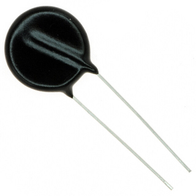
| 描述 | TVS DIODE 30VWM 48.4VC DO204ACTVS 二极管 - 瞬态电压抑制器 500W 30V 5% Unidir |
| 产品分类 | |
| 品牌 | Vishay SemiconductorsVishay Semiconductor Diodes Division |
| 产品手册 | |
| 产品图片 |
|
| rohs | RoHS 合规性豁免无铅 / 符合限制有害物质指令(RoHS)规范要求 |
| 产品系列 | 二极管与整流器,TVS二极管,TVS 二极管 - 瞬态电压抑制器,Vishay Semiconductors SA30A-E3/1TransZorb® |
| 数据手册 | |
| 产品型号 | SA30A-E3/1SA30A-E3/1 |
| 不同频率时的电容 | - |
| 产品目录绘图 |
|
| 产品种类 | TVS 二极管 - 瞬态电压抑制器 |
| 供应商器件封装 | DO-204AC(DO-15) |
| 其它名称 | SA30A-E3/1GI |
| 击穿电压 | 33.3 V to 36.8 V |
| 功率-峰值脉冲 | 500W |
| 包装 | 散装 |
| 单向通道 | 1 |
| 双向通道 | - |
| 商标 | Vishay Semiconductors |
| 安装类型 | 通孔 |
| 安装风格 | Through Hole |
| 封装 | Bulk |
| 封装/外壳 | DO-204AC,DO-15,轴向 |
| 封装/箱体 | DO-204AC |
| 尺寸 | 3.6 mm Dia. x 3.6 mm (Max) W x 7.6 mm L |
| 峰值浪涌电流 | 10 A |
| 峰值脉冲功率耗散 | 500 W |
| 工作温度 | -55°C ~ 175°C |
| 工作电压 | 30 V |
| 工厂包装数量 | 4000 |
| 应用 | 通用 |
| 最大工作温度 | + 175 C |
| 最小工作温度 | - 55 C |
| 极性 | Unidirectional |
| 标准包装 | 4,000 |
| 电压-击穿(最小值) | 33.3V |
| 电压-反向关态(典型值) | 30V |
| 电压-箝位(最大值)@Ipp | 48.4V |
| 电流-峰值脉冲(10/1000µs) | 10A |
| 电源线路保护 | 无 |
| 端接类型 | Axial |
| 类型 | 齐纳 |
| 系列 | SA5.0A through SA170CA |
| 钳位电压 | 48.4 V |


- 商务部:美国ITC正式对集成电路等产品启动337调查
- 曝三星4nm工艺存在良率问题 高通将骁龙8 Gen1或转产台积电
- 太阳诱电将投资9.5亿元在常州建新厂生产MLCC 预计2023年完工
- 英特尔发布欧洲新工厂建设计划 深化IDM 2.0 战略
- 台积电先进制程称霸业界 有大客户加持明年业绩稳了
- 达到5530亿美元!SIA预计今年全球半导体销售额将创下新高
- 英特尔拟将自动驾驶子公司Mobileye上市 估值或超500亿美元
- 三星加码芯片和SET,合并消费电子和移动部门,撤换高东真等 CEO
- 三星电子宣布重大人事变动 还合并消费电子和移动部门
- 海关总署:前11个月进口集成电路产品价值2.52万亿元 增长14.8%


PDF Datasheet 数据手册内容提取
SA5.0A thru SA170CA www.vishay.com Vishay General Semiconductor TRANSZORB® Transient Voltage Suppressors FEATURES • Glass passivated chip junction • Available in uni-directional and bi-directional • 500 W peak pulse power capability with a 10/1000 μs waveform, repetitive rate (duty cycle): 0.01 % • Excellent clamping capability DO-204AC (DO-15) • Very fast response time • Low incremental surge resistance • Solder dip 275 °C max. 10 s, per JESD 22-B106 • AEC-Q101 qualified • Material categorization: For definitions of compliance PRIMARY CHARACTERISTICS please see www.vishay.com/doc?99912 V 5.0 V to 170 V WM TYPICAL APPLICATIONS V (uni-directional) 6.4 V to 209 V BR V (bi-directional) 6.4 V to 209 V Use in sensitive electronics protection against voltage BR transients induced by inductive load switching and lighting P 500 W PPM on ICs, MOSFET, signal lines of sensor units for consumer, PD 3.0 W computer, industrial, and telecommunication. I (uni-directional only) 70 A FSM T max. 175 °C MECHANICAL DATA J Polarity Uni-directional, bi-directional Case: DO-204AC, molded epoxy over passivated chip Molding compound meets UL 94 V-0 flammability rating Package DO-204AC (DO-15) Base P/N-E3 - RoHS compliant, commercial grade Base P/NHE3 - RoHS compliant, AEC-Q101 qualified Terminals: Matte tin plated leads, solderable per DEVICES FOR BI-DIRECTION APPLICATIONS J-STD-002 and JESD 22-B102 For bi-directional types, use CA suffix (e.g. SA5.0CA, E3 suffix meets JESD 201 class 1A whisker test, HE3 suffix SA170CA). meets JESD 201 class 2 whisker test Electrical characteristics apply in both directions. Polarity: For uni-directional types the color band denotes cathode end, no marking on bi-directional types MAXIMUM RATINGS (T = 25 °C unless otherwise noted) A PARAMETER SYMBOL VALUE UNIT Peak pulse power dissipation with a 10/1000 μs waveform (1) (fig. 1) P 500 W PPM Peak pulse current with a 10/1000 μs waveform (1) I See next table A PPM Power dissipation on infinite heatsink at T = 75 °C (fig. 5) P 3.0 W L D Peak forward surge current 10 ms single half sine-wave uni-directional only I 70 A FSM Maximum instantaneous forward voltage at 100 A for uni-directional only (3) V 3.5 V F Operating junction and storage temperature range T , T - 55 to + 175 °C J STG Notes (1) Non-repetitive current pulse, per fig. 3 and derated above T = 25 °C per fig. 2 A (2) 8.3 ms single half sine-wave or equivalent square wave, duty cycle = 4 pulses per minute maximum Revision: 18-Sep-12 1 Document Number: 88378 For technical questions within your region: DiodesAmericas@vishay.com, DiodesAsia@vishay.com, DiodesEurope@vishay.com THIS DOCUMENT IS SUBJECT TO CHANGE WITHOUT NOTICE. THE PRODUCTS DESCRIBED HEREIN AND THIS DOCUMENT ARE SUBJECT TO SPECIFIC DISCLAIMERS, SET FORTH AT www.vishay.com/doc?91000
SA5.0A thru SA170CA www.vishay.com Vishay General Semiconductor ELECTRICAL CHARACTERISTICS (T = 25 °C unless otherwise noted) A BREAKDOWN MAXIMUM MAXIMUM MAXIMUM MAXIMUM VOLTAGE TEST STAND-OFF PEAK REVERSE CLAMPING TEMPERATURE V AT I (1) CURRENT VOLTAGE PULSE DEVICE TYPE BR T LEAKAGE VOLTAGE COEFFICENT (V) I V CURRENT T WM AT V (3) AT I AT V (mA) (V) WM I (2) PPM BR MIN. MAX. ID (μA) PP(AM) VC (V) (%/°C) SA5.0A (4) 6.40 7.07 10 5.0 600 54.3 9.2 5 SA6.0A 6.67 7.37 10 6.0 600 48.5 10.3 5 SA6.5A 7.22 7.98 10 6.5 400 44.7 11.2 5 SA7.0A 7.78 8.60 10 7.0 150 41.7 12.0 6 SA7.5A 8.33 9.21 1.0 7.5 50 38.8 12.9 7 SA8.0A 8.89 9.83 1.0 8.0 25 36.8 13.6 7 SA8.5A 9.44 10.4 1.0 8.5 10 34.7 14.4 8 SA9.0A 10.0 11.1 1.0 9.0 5.0 32.5 15.4 9 SA10A 11.1 12.3 1.0 10 1.0 29.4 17.0 10 SA11A 12.2 13.5 1.0 11 1.0 27.5 18.2 11 SA12A 13.3 14.7 1.0 12 1.0 25.1 19.9 12 SA13A 14.4 15.9 1.0 13 1.0 23.3 21.5 13 SA14A 15.6 17.2 1.0 14 1.0 21.6 23.2 14 SA15A 16.7 18.5 1.0 15 1.0 20.5 24.4 16 SA16A 17.8 19.7 1.0 16 1.0 19.2 26.0 17 SA17A 18.9 20.9 1.0 17 1.0 18.1 27.6 19 SA18A 20.0 22.1 1.0 18 1.0 17.1 29.2 20 SA20A 22.2 24.5 1.0 20 1.0 15.4 32.4 23 SA22A 24.4 26.9 1.0 22 1.0 14.1 35.5 25 SA24A 26.7 29.5 1.0 24 1.0 12.9 38.9 28 SA26A 28.9 31.9 1.0 26 1.0 11.9 42.1 30 SA28A 31.1 34.4 1.0 28 1.0 11 45.4 31 SA30A 33.3 36.8 1.0 30 1.0 10 48.4 36 SA33A 36.7 40.6 1.0 33 1.0 9.4 53.3 39 SA36A 40.0 44.2 1.0 36 1.0 8.6 58.1 41 SA40A 44.4 49.1 1.0 40 1.0 7.8 64.5 46 SA43A 47.8 52.8 1.0 43 1.0 7.2 69.4 50 SA45A 50.0 55.3 1.0 45 1.0 6.9 72.7 52 SA48A 53.3 58.9 1.0 48 1.0 6.5 77.4 56 SA51A 56.7 62.7 1.0 51 1.0 6.1 82.4 61 SA54A 60.0 66.3 1.0 54 1.0 5.7 87.1 65 SA58A 64.4 71.2 1.0 58 1.0 5.3 93.6 70 SA60A 66.7 73.7 1.0 60 1.0 5.2 96.8 71 SA64A 71.1 78.6 1.0 64 1.0 4.9 103 76 SA70A 77.8 86.0 1.0 70 1.0 4.4 113 85 SA75A 83.3 92.1 1.0 75 1.0 4.1 121 91 SA78A 86.7 95.8 1.0 78 1.0 4 126 95 SA85A 94.4 104 1.0 85 1.0 3.6 137 103 SA90A 100 111 1.0 90 1.0 3.4 146 110 SA100A 111 123 1.0 100 1.0 3.1 162 123 SA110A 122 135 1.0 110 1.0 2.8 177 133 SA120A 133 147 1.0 120 1.0 2.6 193 146 SA130A 144 159 1.0 130 1.0 2.4 209 158 SA150A 167 185 1.0 150 1.0 2.1 243 184 SA160A 178 197 1.0 160 1.0 1.9 259 196 SA170A 189 209 1.0 170 1.0 1.8 275 208 Notes (1) Pulse test: tp 50 ms (2) Surge current waveform per fig. 3 and derate per fig. 2 (3) For bi-directional types with V of 10 V and less the I limit is doubled WM D (4) For the bi-directional SA5.0CA, the maximum V is 7.25 V BR (5) All terms and symbols are consistent with ANSI/EEE CA62.35 Revision: 18-Sep-12 2 Document Number: 88378 For technical questions within your region: DiodesAmericas@vishay.com, DiodesAsia@vishay.com, DiodesEurope@vishay.com THIS DOCUMENT IS SUBJECT TO CHANGE WITHOUT NOTICE. THE PRODUCTS DESCRIBED HEREIN AND THIS DOCUMENT ARE SUBJECT TO SPECIFIC DISCLAIMERS, SET FORTH AT www.vishay.com/doc?91000
SA5.0A thru SA170CA www.vishay.com Vishay General Semiconductor ORDERING INFORMATION (Example) PREFERRED PIN UNIT WEIGHT (g) PREFERRED PACKAGE CODE BASE QUANTITY DELIVERY MODE SA5.0A-E3/54 0.432 54 4000 13" diameter paper tape and reel SA5.0AHE3/54 (1) 0.432 54 4000 13" diameter paper tape and reel Note (1) AEC-Q101 qualified RATINGS AND CHARACTERISTICS CURVES (T = 25 °C unless otherwise noted) A 150 30 Non-Repetitive Pulse TJ = 25 °C W) WTa =ve 2fo5r °mC shown in Fig. 3 MSR tr = 10 µs Pisu dlseefi nWeidd tahs ( tthd)e Point ower (k 10 A I % ,tne 100 HaPIlPfe PVaMaklu Vea l-ueI wdehcearyes t htoe 5P0e a%k oCfu IrPrPeMnt ak Pulse P 1.0 ”P0P.K5” td ExImpDopenucelasnyetial rruC esluP IPPM P2P PPe - PPM CPPuPPrKKrentWttaddvefoHStradqm l=ufs aS7r ietnpe kaeP - IMPP 50 td 1a0s /d1e0f0in0e µds b Wy aRv.eEf.oAr.m 0.1 0 0.1 µs 1.0 µs 10 µs 100 µs 1.0 ms 10 ms 0 1.0 2.0 3.0 4.0 td - Pulse Width t - Time (ms) Fig. 1 - Peak Pulse Power Rating Curve Fig. 3 - Pulse Waveform 100 200 ulse Power (P) or Current (I)PPPPDerating in Percentage, % 752505 Peak Forward Surge Current (A) 100 8.3 ms Single Half Sine-Wave Peak P I - FSM 0 10 0 25 50 75 100 125 150 175 200 1 10 100 TJ - Initial Temperature (°C) Number of Cycles at 60 Hz Fig. 4 - Maximum Non-Repetitive Forward Surge Current Fig. 2 - Pulse Derating Curve Uni-Directional Only Revision: 18-Sep-12 3 Document Number: 88378 For technical questions within your region: DiodesAmericas@vishay.com, DiodesAsia@vishay.com, DiodesEurope@vishay.com THIS DOCUMENT IS SUBJECT TO CHANGE WITHOUT NOTICE. THE PRODUCTS DESCRIBED HEREIN AND THIS DOCUMENT ARE SUBJECT TO SPECIFIC DISCLAIMERS, SET FORTH AT www.vishay.com/doc?91000
SA5.0A thru SA170CA www.vishay.com Vishay General Semiconductor 4.0 100 60 Hz Waveform: Resistive or ge SA170 10 x 1000 Impulse a n (W) 3.0 Inductive Load g Volt SA110S A70D VC = VC - VBR patio mpin 10 SA40S A24 er Dissi 2.0 ntal Cla SA15 ow L = 0.375" (9.5 mm) me 1.0 SA9.0 - PD 1.0 Lead Lengths ncre SA5.0 P - IC V 0 0.1 0 25 50 75 100 125 150 175 200 0.5 1 10 50 TL - Lead Temperature (°C) IPP - Peak Pulse Current (A) Fig. 5 - Steady State Power Derating Curve Fig. 8 - Incremental Clamping Voltage Curve Uni-Directional 10 000 100 Waveform: SA170 Uni-Directional e 8 x 20 Impulse SA110 Bi-Directional oltag DVC = VC - VBR SA70 atnce (pF)1000 VR = 0 TfV =Js i g=1 =.20 55 M 0° CHmzVp-p Clamping V 10 SSSSAAAA34620004 aci al SA15 CCap - J 100 VR = Rated crement 1.0 SSAA96..05 Stand-Off voltage n - IC V 10 0.1 5 100 500 0.5 1 10 50 VWM - Reverse Stand-Off Voltage (V) IPP - Peak Pulse Current (A) Fig. 6 - Capacitance Fig. 9 - Incremental Clamping Voltage Curve Bi-Directional 100 100 ge W8 xa v2e0f oImrmp:ulse SA170 SA110 ge W10a xv e1f0o0rm0 :Impulse Volta DVC = VC - VBR SSAA7504 Volta SA170 SA110 DVC = VC - VBR ping 10 SA40 ping 10 SA70 m SA30 m SA40 SA24 a a Cl Cl SA15 ental SSSAAA211458 ental SA9.0 m 1.0 SA12 m 1.0 SA6.5 ncre SSAA59..00 ncre - IC - IC V V 0.1 0.1 0.5 1 10 50 0.5 1 10 50 I - Peak Pulse Current (A) I - Peak Pulse Current (A) PP PP Fig. 7 - Incremental Clamping Voltage Curve Uni-Directional Fig. 10 - Incremental Clamping Voltage Curve Bi-Directional Revision: 18-Sep-12 4 Document Number: 88378 For technical questions within your region: DiodesAmericas@vishay.com, DiodesAsia@vishay.com, DiodesEurope@vishay.com THIS DOCUMENT IS SUBJECT TO CHANGE WITHOUT NOTICE. THE PRODUCTS DESCRIBED HEREIN AND THIS DOCUMENT ARE SUBJECT TO SPECIFIC DISCLAIMERS, SET FORTH AT www.vishay.com/doc?91000
SA5.0A thru SA170CA www.vishay.com Vishay General Semiconductor 100 200 TJ = 25 °C C) Pulse Width = 300 µs V/° 100 nt (A) 1200 1 % Duty Cycle ent (m Uni-Directional Curre oeffici Bi-Directional d C ar e 10 w ur - ForF 21 mperat I e T 0.2 Uni-Directional Only V - 0.1 1.0 0 0.5 1 1.5 2 2.5 5.0 10 100 500 V - Forward Voltage (V) V - Rated Stand-Off Voltage (V) F WM Fig. 11 - Typical Instantaneous Forward Voltage Fig. 12 - Breakdown Voltage Temperature Coefficient Curve PACKAGE OUTLINE DIMENSIONS in inches (millimeters) DO-204AC (DO-15) 0.034 (0.86) 0.028 (0.71) DIA. 1.0 (25.4) MIN. 0.300 (7.6) 0.230 (5.8) 0.140 (3.6) 0.104 (2.6) DIA. 1.0 (25.4) MIN. Revision: 18-Sep-12 5 Document Number: 88378 For technical questions within your region: DiodesAmericas@vishay.com, DiodesAsia@vishay.com, DiodesEurope@vishay.com THIS DOCUMENT IS SUBJECT TO CHANGE WITHOUT NOTICE. THE PRODUCTS DESCRIBED HEREIN AND THIS DOCUMENT ARE SUBJECT TO SPECIFIC DISCLAIMERS, SET FORTH AT www.vishay.com/doc?91000
Legal Disclaimer Notice www.vishay.com Vishay Disclaimer ALL PRODUCT, PRODUCT SPECIFICATIONS AND DATA ARE SUBJECT TO CHANGE WITHOUT NOTICE TO IMPROVE RELIABILITY, FUNCTION OR DESIGN OR OTHERWISE. Vishay Intertechnology, Inc., its affiliates, agents, and employees, and all persons acting on its or their behalf (collectively, “Vishay”), disclaim any and all liability for any errors, inaccuracies or incompleteness contained in any datasheet or in any other disclosure relating to any product. Vishay makes no warranty, representation or guarantee regarding the suitability of the products for any particular purpose or the continuing production of any product. To the maximum extent permitted by applicable law, Vishay disclaims (i) any and all liability arising out of the application or use of any product, (ii) any and all liability, including without limitation special, consequential or incidental damages, and (iii) any and all implied warranties, including warranties of fitness for particular purpose, non-infringement and merchantability. Statements regarding the suitability of products for certain types of applications are based on Vishay’s knowledge of typical requirements that are often placed on Vishay products in generic applications. Such statements are not binding statements about the suitability of products for a particular application. It is the customer’s responsibility to validate that a particular product with the properties described in the product specification is suitable for use in a particular application. Parameters provided in datasheets and/or specifications may vary in different applications and performance may vary over time. All operating parameters, including typical parameters, must be validated for each customer application by the customer’s technical experts. Product specifications do not expand or otherwise modify Vishay’s terms and conditions of purchase, including but not limited to the warranty expressed therein. Except as expressly indicated in writing, Vishay products are not designed for use in medical, life-saving, or life-sustaining applications or for any other application in which the failure of the Vishay product could result in personal injury or death. Customers using or selling Vishay products not expressly indicated for use in such applications do so at their own risk. Please contact authorized Vishay personnel to obtain written terms and conditions regarding products designed for such applications. No license, express or implied, by estoppel or otherwise, to any intellectual property rights is granted by this document or by any conduct of Vishay. Product names and markings noted herein may be trademarks of their respective owners. Material Category Policy Vishay Intertechnology, Inc. hereby certifies that all its products that are identified as RoHS-Compliant fulfill the definitions and restrictions defined under Directive 2011/65/EU of The European Parliament and of the Council of June 8, 2011 on the restriction of the use of certain hazardous substances in electrical and electronic equipment (EEE) - recast, unless otherwise specified as non-compliant. Please note that some Vishay documentation may still make reference to RoHS Directive 2002/95/EC. We confirm that all the products identified as being compliant to Directive 2002/95/EC conform to Directive 2011/65/EU. Vishay Intertechnology, Inc. hereby certifies that all its products that are identified as Halogen-Free follow Halogen-Free requirements as per JEDEC JS709A standards. Please note that some Vishay documentation may still make reference to the IEC 61249-2-21 definition. We confirm that all the products identified as being compliant to IEC 61249-2-21 conform to JEDEC JS709A standards. Revision: 02-Oct-12 1 Document Number: 91000