ICGOO在线商城 > 分立半导体产品 > 晶体管 - FET,MOSFET - 单 > RTM002P02T2L
 Datasheet下载
- 型号: RTM002P02T2L
- 制造商: ROHM Semiconductor
- 库位|库存: xxxx|xxxx
- 要求:
| 数量阶梯 | 香港交货 | 国内含税 |
| +xxxx | $xxxx | ¥xxxx |
查看当月历史价格
查看今年历史价格
RTM002P02T2L产品简介:
ICGOO电子元器件商城为您提供RTM002P02T2L由ROHM Semiconductor设计生产,在icgoo商城现货销售,并且可以通过原厂、代理商等渠道进行代购。 RTM002P02T2L价格参考¥0.47-¥0.82。ROHM SemiconductorRTM002P02T2L封装/规格:晶体管 - FET,MOSFET - 单, 表面贴装 P 沟道 20V 200mA(Ta) 150mW(Ta) VMT3。您可以下载RTM002P02T2L参考资料、Datasheet数据手册功能说明书,资料中有RTM002P02T2L 详细功能的应用电路图电压和使用方法及教程。
RTM002P02T2L 是由罗姆半导体(Rohm Semiconductor)生产的一款单通道 MOSFET(金属氧化物场效应晶体管)。该器件属于 N 沟道增强型 MOSFET,具有低导通电阻和高开关速度的特点,适用于多种电力电子应用。

 应用场景

1. 电源管理:
   RTM002P02T2L 由于其低导通电阻特性,非常适合用于 DC-DC 转换器、线性稳压器等电源管理电路中。它可以有效地降低功耗,提高电源转换效率,特别适用于需要高效能和小尺寸设计的便携式设备,如智能手机、平板电脑和其他消费电子产品。

2. 负载开关:
   在需要频繁切换负载的应用中,如 USB 端口保护、电池充电电路等,RTM002P02T2L 可以作为负载开关使用。它能够快速响应并提供低损耗的电流路径,确保系统在不同工作状态下的稳定性和可靠性。

3. 电机驱动:
   对于小型直流电机或步进电机的驱动,RTM002P02T2L 可以作为功率级元件,控制电机的启动、停止和调速。其低导通电阻有助于减少发热,延长电机和驱动电路的使用寿命。

4. 信号切换:
   在通信设备和测试仪器中,RTM002P02T2L 可用于信号切换电路,实现不同信号路径的选择。其高开关速度和低寄生电容使其能够在高频信号处理中保持良好的性能。

5. 过流保护:
   该 MOSFET 还可以用于过流保护电路中,通过检测电流并在超过设定阈值时迅速关断,从而保护下游电路免受过载损害。其内置的体二极管可以在反向电压条件下提供额外的保护功能。

总之,RTM002P02T2L 凭借其优异的电气特性和紧凑的封装形式,广泛应用于各种需要高效、可靠电力传输和控制的场合,特别是在便携式设备和小型化电子产品中表现尤为突出。
| 参数 | 数值 |
| 产品目录 | |
| ChannelMode | Enhancement |
| 描述 | MOSFET P-CH 20V 200MA VMT3MOSFET P-CH 20V 200MA |
| 产品分类 | FET - 单分离式半导体 |
| FET功能 | 标准 |
| FET类型 | MOSFET P 通道,金属氧化物 |
| Id-ContinuousDrainCurrent | +/- 200 mA |
| Id-连续漏极电流 | 200 mA |
| 品牌 | Rohm Semiconductor |
| 产品手册 | |
| 产品图片 |
|
| rohs | 符合RoHS无铅 / 符合限制有害物质指令(RoHS)规范要求 |
| 产品系列 | 晶体管,MOSFET,ROHM Semiconductor RTM002P02T2L- |
| 数据手册 | |
| 产品型号 | RTM002P02T2L |
| Pd-PowerDissipation | 0.15 W |
| Pd-功率耗散 | 150 mW |
| RdsOn-Drain-SourceResistance | 2 Ohms |
| RdsOn-漏源导通电阻 | 2 Ohms |
| Vds-Drain-SourceBreakdownVoltage | - 20 V |
| Vds-漏源极击穿电压 | - 20 V |
| Vgs-Gate-SourceBreakdownVoltage | +/- 12 V |
| Vgs-栅源极击穿电压 | 12 V |
| 上升时间 | 6 ns |
| 下降时间 | 6 ns |
| 不同Id时的Vgs(th)(最大值) | 2V @ 1mA |
| 不同Vds时的输入电容(Ciss) | 50pF @ 10V |
| 不同Vgs时的栅极电荷(Qg) | - |
| 不同 Id、Vgs时的 RdsOn(最大值) | 1.5 欧姆 @ 200mA,4.5V |
| 产品培训模块 | http://www.digikey.cn/PTM/IndividualPTM.page?site=cn&lang=zhs&ptm=24809 |
| 产品目录绘图 |
|
| 产品目录页面 | |
| 产品种类 | MOSFET |
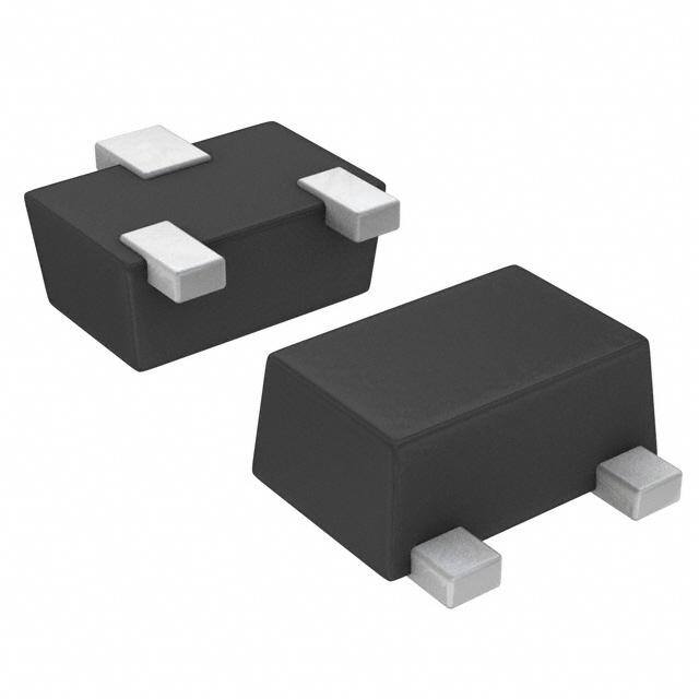
| 供应商器件封装 | VMT3 |
| 其它名称 | RTM002P02T2LTR |
| 典型关闭延迟时间 | 35 ns |
| 功率-最大值 | 150mW |
| 包装 | 带卷 (TR) |
| 商标 | ROHM Semiconductor |
| 安装类型 | 表面贴装 |
| 安装风格 | SMD/SMT |
| 封装 | Reel |
| 封装/外壳 | SOT-723 |
| 封装/箱体 | VMT-3 |
| 工具箱 | /product-detail/zh/846-1002-KIT/846-1002-KIT-ND/2277303 |
| 工厂包装数量 | 8000 |
| 晶体管极性 | P-Channel |
| 标准包装 | 8,000 |
| 漏源极电压(Vdss) | 20V |
| 特色产品 | http://www.digikey.com/cn/zh/ph/ROHM/MOSFET_ECOMOS.html |
| 电流-连续漏极(Id)(25°C时) | 200mA (Ta) |
| 通道模式 | Enhancement |
| 配置 | Single |


- 商务部:美国ITC正式对集成电路等产品启动337调查
- 曝三星4nm工艺存在良率问题 高通将骁龙8 Gen1或转产台积电
- 太阳诱电将投资9.5亿元在常州建新厂生产MLCC 预计2023年完工
- 英特尔发布欧洲新工厂建设计划 深化IDM 2.0 战略
- 台积电先进制程称霸业界 有大客户加持明年业绩稳了
- 达到5530亿美元!SIA预计今年全球半导体销售额将创下新高
- 英特尔拟将自动驾驶子公司Mobileye上市 估值或超500亿美元
- 三星加码芯片和SET,合并消费电子和移动部门,撤换高东真等 CEO
- 三星电子宣布重大人事变动 还合并消费电子和移动部门
- 海关总署:前11个月进口集成电路产品价值2.52万亿元 增长14.8%


PDF Datasheet 数据手册内容提取
RTM002P02 Transistors 2.5V Drive Pch MOS FET RTM002P02 (cid:122)Structure (cid:122)External dimensions (Unit : mm) Silicon P-channel MOS FET VMT3 1.2 (cid:122)Features 0.32 2 0. 1) Low On-resistance. (3) 82 2) Small package (VMT3). 0.1. 0.22 (1)(2) 3) 2.5V drive. 0.40.4 0.2 0.50.13 0.8 (1)Gate (2)Source (cid:122)Applications (3)Drain Abbreviated symbol : TW Switching (cid:122)Packaging specifications (cid:122)Inner circuit Package Taping (3) Type Code T2L Basic ordering unit (pieces) 8000 RTM002P02 (1) ∗2 ∗1 (2) (1) Gate ∗1 ESD PROTECTION DIODE (2) Source ∗2 BODY DIODE (3) Drain (cid:122)Absolute maximum ratings (Ta=25°C) Parameter Symbol Limits Unit Drain-source voltage VDSS −20 V Gate-source voltage VGSS ±12 V Continuous ID ±0.2 A Drain current Pulsed IDP ∗1 ±0.4 A Total power dissipation PD ∗2 0.15 W Channel temperature Tch 150 °C Range of storage temperature Tstg −55 to +150 °C ∗1 Pw≤10µs, Duty cycle≤1% ∗2 Each terminal mounted on a recommended land (cid:122)Thermal resistance Parameter Symbol Limits Unit Channel to ambient Rth(ch-a)∗ 833 °C/W ∗ Each terminal mounted on a recommended land 1/2
RTM002P02 Transistors (cid:122)Electrical characteristics (Ta=25°C) Parameter Symbol Min. Typ. Max. Unit Conditions Gate-source leakage IGSS − − ±10 µA VGS= ±12V, VDS=0V Drain-source breakdown voltage V(BR) DSS −20 − − V ID= −1mA, VGS=0V Zero gate voltage drain current IDSS − − −1 µA VDS= −20V, VGS=0V Gate threshold voltage VGS (th) −0.7 − −2.0 V VDS= −10V, ID= −1mA − 1.0 1.5 Ω ID= −0.2A, VGS= −4.5V Sretsaitsicta dnrcaein-source on-state RDS (on)∗ − 1.1 1.6 Ω ID= −0.2A, VGS= −4V − 2.0 3.0 Ω ID= −0.15A, VGS= −2.5V Forward transfer admittance Yfs ∗ 0.2 − − S VDS= −10V, ID= −0.15A Input capacitance Ciss − 50 − pF VDS= −10V Output capacitance Coss − 5 − pF VGS= 0V Reverse transfer capacitance Crss − 5 − pF f=1MHz Turn-on delay time td (on) ∗ − 9 − ns VDD −15V RTuisren -toimff edelay time td t(roff) ∗∗ −− 365 −− nnss IRVDGL==S =− 10 −0.1405.Ω5AV Fall time tf ∗ − 45 − ns RG= 10Ω ∗Pulsed (cid:122)Body diode characteristics (Source-drain) (Ta=25°C) Parameter Symbol Min. Typ. Max. Unit Conditions Forward voltage VSD − − −1.2 V IS= −0.1A, VGS=0V 2/2
Appendix Notes No technical content pages of this document may be reproduced in any form or transmitted by any means without prior permission of ROHM CO.,LTD. The contents described herein are subject to change without notice. The specifications for the product described in this document are for reference only. Upon actual use, therefore, please request that specifications to be separately delivered. Application circuit diagrams and circuit constants contained herein are shown as examples of standard use and operation. Please pay careful attention to the peripheral conditions when designing circuits and deciding upon circuit constants in the set. Any data, including, but not limited to application circuit diagrams information, described herein are intended only as illustrations of such devices and not as the specifications for such devices. ROHM CO.,LTD. disclaims any warranty that any use of such devices shall be free from infringement of any third party's intellectual property rights or other proprietary rights, and further, assumes no liability of whatsoever nature in the event of any such infringement, or arising from or connected with or related to the use of such devices. Upon the sale of any such devices, other than for buyer's right to use such devices itself, resell or otherwise dispose of the same, no express or implied right or license to practice or commercially exploit any intellectual property rights or other proprietary rights owned or controlled by ROHM CO., LTD. is granted to any such buyer. Products listed in this document are no antiradiation design. The products listed in this document are designed to be used with ordinary electronic equipment or devices (such as audio visual equipment, office-automation equipment, communications devices, electrical appliances and electronic toys). Should you intend to use these products with equipment or devices which require an extremely high level of reliability and the malfunction of with would directly endanger human life (such as medical instruments, transportation equipment, aerospace machinery, nuclear-reactor controllers, fuel controllers and other safety devices), please be sure to consult with our sales representative in advance. About Export Control Order in Japan Products described herein are the objects of controlled goods in Annex 1 (Item 16) of Export Trade Control Order in Japan. In case of export from Japan, please confirm if it applies to "objective" criteria or an "informed" (by MITI clause) on the basis of "catch all controls for Non-Proliferation of Weapons of Mass Destruction. Appendix1-Rev1.1