ICGOO在线商城 > 集成电路(IC) > PMIC - 稳压器 - 线性 > RT9064-33GV

 Datasheet下载
- 型号: RT9064-33GV
- 制造商: RICHTEK
- 库位|库存: xxxx|xxxx
- 要求:
| 数量阶梯 | 香港交货 | 国内含税 |
| +xxxx | $xxxx | ¥xxxx |
查看当月历史价格
查看今年历史价格
RT9064-33GV产品简介:
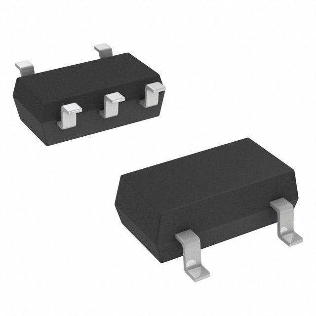
ICGOO电子元器件商城为您提供RT9064-33GV由RICHTEK设计生产,在icgoo商城现货销售,并且可以通过原厂、代理商等渠道进行代购。 RT9064-33GV价格参考。RICHTEKRT9064-33GV封装/规格:PMIC - 稳压器 - 线性, Linear Voltage Regulator IC Positive Fixed 1 Output 3.3V 200mA SOT-23-3。您可以下载RT9064-33GV参考资料、Datasheet数据手册功能说明书,资料中有RT9064-33GV 详细功能的应用电路图电压和使用方法及教程。
| 参数 | 数值 |
| 产品目录 | 集成电路 (IC) |
| 描述 | IC REG LDO 3.3V 0.2A |
| 产品分类 | |
| 品牌 | Richtek USA Inc |
| 数据手册 | http://www.richtek.com/download_ds.jsp?s=1122 |
| 产品图片 | |
| 产品型号 | RT9064-33GV |
| rohs | 无铅 / 符合限制有害物质指令(RoHS)规范要求 |
| 产品系列 | - |
| 供应商器件封装 | SOT-23-3 |
| 其它名称 | 1028-1310-6 |
| 包装 | Digi-Reel® |
| 安装类型 | 表面贴装 |
| 封装/外壳 | TO-236-3,SC-59,SOT-23-3 |
| 工作温度 | -40°C ~ 85°C |
| 标准包装 | 1 |
| 电压-跌落(典型值) | - |
| 电压-输入 | 3.5 V ~ 14 V |
| 电压-输出 | 3.3V |
| 电流-输出 | 200mA |
| 电流-限制(最小值) | 240mA |
| 稳压器拓扑 | 正,固定式 |
| 稳压器数 | 1 |


PDF Datasheet 数据手册内容提取
® RT9064 Ultra Low Power, 14V, 200mA Low-Dropout Linear Regulator General Description Features The RT9064 is a low-dropout (LDO) linear regulator that 2μμμμμA Quiescent Current features high input voltage, low dropout voltage, ultra-low ±±±±±2% Output Accuracy operating current, and miniaturized packaging. With 200mA Output Current quiescent current as low as 2μA, the RT9064 is ideal for 14V Maximum Operating Input Voltage battery-powered equipment. Dropout Voltage : 0.4V at 100mA Fixed Output Voltage : 2.5V/3.3V/5V The RT9064's stability requirements are easily met with Stable with Ceramic or Tantalum Capacitor all types of output capacitors, including tiny ceramic Current Limit Protection capacitors, over its wide input range (3.5V to 14V) and its Over-Temperature Protection load current range (0mA to 200mA). The RT9064 offers SOT-23-3, SOT-89-3 Packages standard output voltages of 2.5V, 3.3V and 5V. RoHS Compliant and Halogen Free Pin Configurations Applications (TOP VIEW) Portable, Battery Powered Equipment GND Ultra Low Power Microcontrollers 3 Ordering and Marking Information 2 Output Marking VCC VOUT Part Number Package Voltage Information SOT-23-3 RT9064-25GV SOT-23-3 0D= VCC RT9064-25GVN 2.5V SOT-23-3 (N) 30= 3 RT9064-25GX SOT-89-3 04= 2 RT9064-33GV SOT-23-3 0E= GND VOUT RT9064-33GVN 3.3V SOT-23-3 (N) 2Z= SOT-23-3 (N-Type) RT9064-33GX SOT-89-3 05= RT9064-50GV SOT-23-3 0F= RT9064-50GVN 5.0V SOT-23-3 (N) 2Y= RT9064-50GX SOT-89-3 06= 2 3 VCC GND VOUT SOT-89-3 Simplified Application Circuit RT9064 VCC VCC VOUT VOUT CIN GND COUT Copyright © 2016 Richtek Technology Corporation. All rights reserved. is a registered trademark of Richtek Technology Corporation. DS9064-01 February 2016 www.richtek.com 1
RT9064 Functional Pin Description Pin No. Pin Name Pin Function SOT-23-3 SOT-23-3 (N-Type) SOT-89-3 1 3 1 VCC Supply Voltage Input. 2 2 3 VOUT Output of the Regulator. 3 1 2 GND Ground. Function Block Diagram VCC VOUT OCP R1 OTP - + GND Bandgap R2 Reference Operation The RT9064 is a high input voltage linear regulator Current Limit specifically designed to minimize external components. The RT9064 provides a current limit function to prevent The minimum required output capacitance for stable damage during output over-load or shorted-circuit operation is 1μF effective capacitance after consideration conditions. The output current is detected by an internal of the temperature and voltage coefficient of the capacitor. sensing transistor. Output Transistor Over-Temperature Protection The RT9064 includes a built-in low on-resistance The over-temperature protection function will turn off the P-MOSFET output transistor for low dropout voltage P-MOSFET when the internal junction temperature applications. exceeds 150°C (typ.) and the output current exceeds 30mA. Once the junction temperature cools down by Error Amplifier approximately 20°C, the regulator will automatically The Error Amplifier compares the output feedback voltage resume operation. from an internal feedback voltage divider to an internal reference voltage and controls the P-MOSFET's gate voltage to maintain output voltage regulation. Copyright © 2016 Richtek Technology Corporation. All rights reserved. is a registered trademark of Richtek Technology Corporation. www.richtek.com DS9064-01 February 2016 2
RT9064 Absolute Maximum Ratings (Note 1) VCC to GND ----------------------------------------------------------------------------------------------------------------- −0.3V to 15V VOUT to VCC --------------------------------------------------------------------------------------------------------------- −14V to 0.3V VOUT to GND --------------------------------------------------------------------------------------------------------------- −0.3V to 6V Power Dissipation, P @ T = 25°C D A SOT-23-3 --------------------------------------------------------------------------------------------------------------------- 0.41W SOT-89-3 --------------------------------------------------------------------------------------------------------------------- 0.59W Package Thermal Resistance (Note 2) SOT-23-3, θ ---------------------------------------------------------------------------------------------------------------- 243.3°C/W JA SOT-89-3, θ ---------------------------------------------------------------------------------------------------------------- 167.7°C/W JA Lead Temperature (Soldering, 10 sec.)-------------------------------------------------------------------------------- 260°C Junction Temperature------------------------------------------------------------------------------------------------------ 150°C Storage Temperature Range --------------------------------------------------------------------------------------------- −65°C to 150°C ESD Susceptibility (Note 3) HBM (Human Body Model)----------------------------------------------------------------------------------------------- 2kV MM (Machine Model) ------------------------------------------------------------------------------------------------------ 200V Recommended Operating Conditions (Note 4) Supply Input Voltage, VCC----------------------------------------------------------------------------------------------- 3.5V to 14V Junction Temperature Range--------------------------------------------------------------------------------------------- −40°C to 125°C Ambient Temperature Range--------------------------------------------------------------------------------------------- −40°C to 85°C Electrical Characteristics ((VOUT + 1V) < VCC < 14V, TA = 25°C, unless otherwise specified.) Parameter Symbol Test Conditions Min Typ Max Unit Output Voltage Range V 2.5 -- 5 V OUT DC Output Accuracy ILOAD = 1mA, VCC = VOUT + 0.5V 2 -- 2 % I = 100mA, V 4.5V -- 0.4 1.2 LOAD OUT Dropout Voltage V V Drop ILOAD =100mA, VOUT < 4.5V -- -- 1.5 Quiescent Current I V = 5V, I = 0A -- 2 4 A Q CC LOAD ILOAD = 1mA, 3.5V VCC < 5.5V -- 0.1 0.2 Line Regulation VLINE % ILOAD = 1mA, 5.5V VCC 14V -- 0.1 0.3 Load Regulation V I = 1mA to 200mA -- 0.5 1 % LOAD LOAD Output Current Limit ILIM VOUT = 0.5 x VOUT(Normal) , VCC = 5V 240 320 400 mA Power Supply Rejection f = 100Hz, ILOAD = 100mA -- 60 -- PSRR dB Ratio f = 10kHz, ILOAD = 100mA -- 40 -- 27 x Output Noise Voltage VON BW = 10Hz to 100kHz , COUT = 1F -- -- VRMS VOUT Startup Time tSTR VOUT = 3V, RL = 30 -- 500 -- s OTP Threshold -- 150 -- C OTP Hysteresis -- 20 -- C Copyright © 2016 Richtek Technology Corporation. All rights reserved. is a registered trademark of Richtek Technology Corporation. DS9064-01 February 2016 www.richtek.com 3
RT9064 Note 1. Stresses beyond those listed “Absolute Maximum Ratings” may cause permanent damage to the device. These are stress ratings only, and functional operation of the device at these or any other conditions beyond those indicated in the operational sections of the specifications is not implied. Exposure to absolute maximum rating conditions may affect device reliability. Note 2. θJA is measured at TA= 25°C on a high effective thermal conductivity four-layer test board per JEDEC 51-7. Note 3. Devices are ESD sensitive. Handling precaution is recommended. Note 4. The device is not guaranteed to function outside its operating conditions. Typical Application Circuit RT9064 VCC CIN VCC VOUT COUT VOUT 1µF GND (Effective Capacitance 1µF) Copyright © 2016 Richtek Technology Corporation. All rights reserved. is a registered trademark of Richtek Technology Corporation. www.richtek.com DS9064-01 February 2016 4
RT9064 Typical Operating Characteristics Output Voltage vs. Temperature Output Voltage vs. Output Current 2.52 2.52 VCC = 12V, ILOAD = 0.1mA 2.51 VCC = 12V, ILOAD = 20mA 2.51 ) VCC = 12V, ILOAD = 50mA ) e (V 2.50 e (V 2.50 VCC = 5V g g a a olt 2.49 olt 2.49 V V ut ut utp 2.48 VCC = 5V, ILOAD = 0.1mA utp 2.48 VCC = 12V O O VCC = 5V, ILOAD = 20mA 2.47 VCC = 5V, ILOAD = 50mA 2.47 VOUT = 2.5V VOUT = 2.5V 2.46 2.46 -50 -25 0 25 50 75 100 125 0 20 40 60 80 100 120 140 160 180 200 Temperature (°C) Output Current (mA) Output Voltage vs. Input Voltage Quiescent Current vs. Temperature 2.52 2.80 2.51 A) 2.54 ) µ e (V 2.50 nt ( oltag 2.49 ILOAD = 0mA Curre 2.28 VCC = 5V put V IILLOOAADD == 100.1mmAA cent 2.02 Out 2.48 IILLOOAADD == 2500mmAA uies VCC = 12V Q 1.76 2.47 VCC = 5V to 13.2V, VOUT = 2.5V VOUT = 2.5V 2.46 1.50 5 6 7 8 9 10 11 12 13 14 -50 -25 0 25 50 75 100 125 Input Voltage (V) Temperature (°C) Quiescent Current vs. Input Voltage Dropout Voltage vs. Temperature 2.16 0.40 2.14 0.35 A) VOUT = 5V µ V) nt ( 2.12 e ( 0.30 e g Curr 2.10 Volta 0.25 scent 2.08 pout 0.20 Quie 2.06 VOUT = 2.5V Dro 0.15 2.04 VCC = 5V, VOUT = 2.5V, ILOAD = 50mA 2.02 0.10 5 6 7 8 9 10 11 12 13 14 -50 -25 0 25 50 75 100 125 Input Voltage (V) Temperature (°C) Copyright © 2016 Richtek Technology Corporation. All rights reserved. is a registered trademark of Richtek Technology Corporation. DS9064-01 February 2016 www.richtek.com 5
RT9064 Current Limit vs. Temperature PSRR vs. Frequency 0.5 0 VCC = 12V, VOUT = 5V VCC = 12V, VOUT = 2.5V, ILOAD = 100mA 0.4 -20 ) A mit ( 0.3 dB) nt Li RR ( -40 e 0.2 S rr P u C -60 0.1 0.0 -80 -50 -25 0 25 50 75 100 125 10 1000 100000 Temperature (°C) Frequency (Hz) Load Transient Response Line Transient Response VOUT (50mV/Div) VCC (5V/Div) ILOAD VOUT (100mA/Div) (20mV/Div) VCC = 12V, VOUT = 2.5V, ILOAD = 10mA to 100mA VCC = 6V to 12V, VOUT = 2.5V, ILOAD = 100mA Time (500μs/Div) Time (250μs/Div) Ground Current vs. Load Current Power Up Response 200 VCC = 12V, VOUT = 2.5V A) 150 VCC µ (10V/Div) nt ( e rr u 100 nd C RRiissiinngg,, TTAA == 2152°5C°C VOUT ou Rising, TA = −40°C (1V/Div) Gr 50 ILOAD (50mA/Div) VCC = 12V, VOUT = 2.5V, ILOAD = 100mA 0 0.001 0.01 0.1 1 10 100 1000 Time (25μs/Div) Load Current (mA) Copyright © 2016 Richtek Technology Corporation. All rights reserved. is a registered trademark of Richtek Technology Corporation. www.richtek.com DS9064-01 February 2016 6
RT9064 Applications Information Like any low dropout linear regulator, the RT9064's external 1.0 ) 1 Four-Layer PCB input and output capacitors must be properly selected for W stability and performance. Use a 1μF or larger input on ( 0.8 capacitor and place it close to the IC's VCC and GND pins. pati SOT-89-3 Any output capacitor meeting the minimum 1mΩ ESR Dissi 0.6 r SOT-23-3 (Equivalent Series Resistance) and effective capacitance e w 0.4 larger than 1μF requirement may be used. Place the output Po m capacitor close to the IC's VOUT and GND pins. Increasing u m 0.2 capacitance and decreasing ESR can improve the circuit's xi a PSRR and line transient response. M 0.0 0 25 50 75 100 125 Thermal Considerations Ambient Temperature (°C) For continuous operation, do not exceed absolute the Figure 1. Derating Curve of Maximum Power Dissipation maximum junction temperature. The maximum power dissipation depends on the thermal resistance of the IC package, PCB layout, rate of surrounding airflow, and the allowed difference between the junction and ambient temperatures. The maximum power dissipation can be calculated by the following formula : P = (T − T ) / θ D(MAX) J(MAX) A JA where T is the maximum junction temperature, T is J(MAX) A the ambient temperature, and θ is the junction to ambient JA thermal resistance. The recommended operating conditions specify a maximum junction temperature is 125°C. The junction to ambient thermal resistance, θ , is layout dependent. On JA a standard JEDEC 51-7 four-layer thermal test board, the thermal resistance, θ , of the SOT-23-3 package is JA 243.3°C/W. For the SOT-89-3 package, the θ , is JA 167.7°C/W. The maximum power dissipation at T = 25°C A can be calculated by the following formula : P = (125°C − 25°C) / (243.3°C/W) = 0.41W for D(MAX) SOT-23-3 package P = (125°C − 25°C) / (167.7°C/W) = 0.59W for D(MAX) SOT-89-3 package For a fixed T of 125°C, the maximum power J(MAX) dissipation depends on the operating ambient temperature and the package's thermal resistance, θ . The derating JA curve in Figure 1 shows the effect of rising ambient temperature on the maximum recommended power dissipation. Copyright © 2016 Richtek Technology Corporation. All rights reserved. is a registered trademark of Richtek Technology Corporation. DS9064-01 February 2016 www.richtek.com 7
RT9064 Outline Dimension H D L C B e A A1 b Dimensions In Millimeters Dimensions In Inches Symbol Min Max Min Max A 0.889 1.295 0.035 0.051 A1 0.000 0.152 0.000 0.006 B 1.397 1.803 0.055 0.071 b 0.356 0.508 0.014 0.020 C 2.591 2.997 0.102 0.118 D 2.692 3.099 0.106 0.122 e 1.803 2.007 0.071 0.079 H 0.080 0.254 0.003 0.010 L 0.300 0.610 0.012 0.024 SOT-23-3 Surface Mount Package Copyright © 2016 Richtek Technology Corporation. All rights reserved. is a registered trademark of Richtek Technology Corporation. www.richtek.com DS9064-01 February 2016 8
RT9064 D D1 A B C C1 e e H A b b b1 Dimensions In Millimeters Dimensions In Inches Symbol Min Max Min Max A 1.397 1.600 0.055 0.063 b 0.356 0.483 0.014 0.019 B 2.388 2.591 0.094 0.102 b1 0.406 0.533 0.016 0.021 C 3.937 4.242 0.155 0.167 C1 0.787 1.194 0.031 0.047 D 4.394 4.597 0.173 0.181 D1 1.397 1.753 0.055 0.069 e 1.448 1.549 0.057 0.061 H 0.356 0.432 0.014 0.017 3-Lead SOT-89 Surface Mount Package Richtek Technology Corporation 14F, No. 8, Tai Yuen 1st Street, Chupei City Hsinchu, Taiwan, R.O.C. Tel: (8863)5526789 Richtek products are sold by description only. Richtek reserves the right to change the circuitry and/or specifications without notice at any time. Customers should obtain the latest relevant information and data sheets before placing orders and should verify that such information is current and complete. Richtek cannot assume responsibility for use of any circuitry other than circuitry entirely embodied in a Richtek product. Information furnished by Richtek is believed to be accurate and reliable. However, no responsibility is assumed by Richtek or its subsidiaries for its use; nor for any infringements of patents or other rights of third parties which may result from its use. No license is granted by implication or otherwise under any patent or patent rights of Richtek or its subsidiaries. DS9064-01 February 2016 www.richtek.com 9