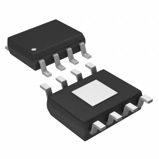
ICGOO在线商城 > 集成电路(IC) > PMIC - 稳压器 - 线性 > RT9018A-25GSP
- 型号: RT9018A-25GSP
- 制造商: RICHTEK
- 库位|库存: xxxx|xxxx
- 要求:
| 数量阶梯 | 香港交货 | 国内含税 |
| +xxxx | $xxxx | ¥xxxx |
查看当月历史价格
查看今年历史价格
RT9018A-25GSP产品简介:
ICGOO电子元器件商城为您提供RT9018A-25GSP由RICHTEK设计生产,在icgoo商城现货销售,并且可以通过原厂、代理商等渠道进行代购。 RT9018A-25GSP价格参考。RICHTEKRT9018A-25GSP封装/规格:PMIC - 稳压器 - 线性, Linear Voltage Regulator IC 1 Output 3A 8-SOP-EP。您可以下载RT9018A-25GSP参考资料、Datasheet数据手册功能说明书,资料中有RT9018A-25GSP 详细功能的应用电路图电压和使用方法及教程。
| 参数 | 数值 |
| 产品目录 | 集成电路 (IC) |
| 描述 | IC REG LDO 2.5V/ADJ 3A 8SOP |
| 产品分类 | |
| 品牌 | Richtek USA Inc |
| 数据手册 | http://www.richtek.com/download_ds.jsp?s=229 |
| 产品图片 |
|
| 产品型号 | RT9018A-25GSP |
| rohs | 无铅 / 符合限制有害物质指令(RoHS)规范要求 |
| RoHS指令信息 | http://www.richtek.com/download.jsp?t=UyUyRmFzc2V0cyUyRjIwMDklMkYwNiUyRjE3JTJGcGFnZTY1MTYwenRpeGIucGRmJTNEJTNEJTNE%0AR0w5NTI1LUMtLVBiLWZyZWUrUHJvZHVjdCsrR3JlZW4rUHJvZHVjdCtTdGF0ZW1lbnQrMDkwNjE2%0AQw%3D%3D |
| 产品系列 | - |
| 供应商器件封装 | 8-SOP-EP |
| 其它名称 | 1028-1058-1 |
| 包装 | 剪切带 (CT) |
| 安装类型 | 表面贴装 |
| 封装/外壳 | 8-SOIC(0.154",3.90mm 宽)裸焊盘 |
| 工作温度 | -40°C ~ 85°C |
| 标准包装 | 1 |
| 电压-跌落(典型值) | 0.21V @ 3A |
| 电压-输入 | 1.4 V ~ 5.5 V |
| 电压-输出 | 2.5V,可调 |
| 电流-输出 | 3A |
| 电流-限制(最小值) | 3.2A |
| 稳压器拓扑 | 正,固定式或可调式 |
| 稳压器数 | 1 |




- 商务部:美国ITC正式对集成电路等产品启动337调查
- 曝三星4nm工艺存在良率问题 高通将骁龙8 Gen1或转产台积电
- 太阳诱电将投资9.5亿元在常州建新厂生产MLCC 预计2023年完工
- 英特尔发布欧洲新工厂建设计划 深化IDM 2.0 战略
- 台积电先进制程称霸业界 有大客户加持明年业绩稳了
- 达到5530亿美元!SIA预计今年全球半导体销售额将创下新高
- 英特尔拟将自动驾驶子公司Mobileye上市 估值或超500亿美元
- 三星加码芯片和SET,合并消费电子和移动部门,撤换高东真等 CEO
- 三星电子宣布重大人事变动 还合并消费电子和移动部门
- 海关总署:前11个月进口集成电路产品价值2.52万亿元 增长14.8%



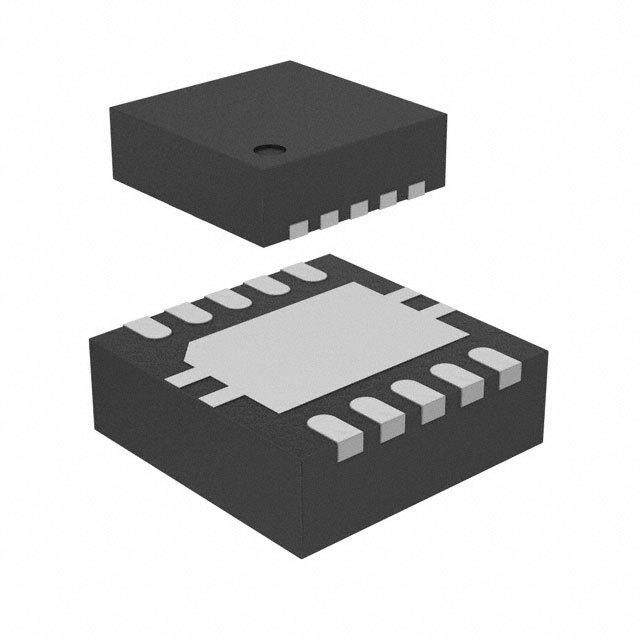
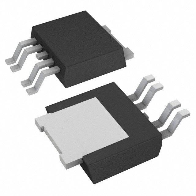
PDF Datasheet 数据手册内容提取
RT9018A/B Maximum 3A, Ultra Low Dropout Regulator General Description Features The RT9018A/B is a high performance positive voltage (cid:122)(cid:122)(cid:122)(cid:122)(cid:122) Maximum 3A Low-Dropout Voltage Regulator regulator designed for use in applications requiring very (cid:122)(cid:122)(cid:122)(cid:122)(cid:122) High Accuracy Output Voltage ±±±±±1.5% low Input voltage and very low dropout voltage at up to (cid:122)(cid:122)(cid:122)(cid:122)(cid:122) Typically 220mV Dropout at 3A 3A(Peak). It operates with a VIN as low as 1.4V and VDD (cid:122)(cid:122)(cid:122)(cid:122)(cid:122) Power Good Output voltage 3V with output voltage programmable as low as (cid:122)(cid:122)(cid:122)(cid:122)(cid:122) Output Voltage Pull Low Resistance when Disable 0.8V. The significant feature includes ultra low dropout, (cid:122)(cid:122)(cid:122)(cid:122)(cid:122) Thermal and Over Current Protection ideal for applications where VOUT is very close to VIN. (cid:122)(cid:122)(cid:122)(cid:122)(cid:122) RoHS Compliant and 100% Lead (Pb)-Free Additionally, there is an enable pin to further reduce power Applications dissipation while shutdown. The RT9018A/B provides excellent regulation over variations in line, load and (cid:122) Front Side Bus VTT (1.2V/3A) temperature. and provides a power OK signal to indicate (cid:122) NoteBook PC Applications if the voltage level of Vo reaches 90% of its rating value. (cid:122) Motherboard Applications The RT9018A/B is available in the SOP-8 (Exposed Pad) Marking Information and WDFN-10L 3x3 packages with 1V, 1.05V, 1.2V, 1.5V, For marking information, contact our sales representative 1.8V and 2.5V internally preset outputs that are also directly or through a Richtek distributor located in your adjustable using external resistors. area, otherwise visit our website for detail. Ordering Information Pin Configurations RT9018A/B- Package Type (TOP VIEW) SP : SOP-8 (Exposed Pad-Option 1) QW : WDFN-10L 3x3 PGOOD 8 GND Operating Temperature Range EN 2 7 ADJ GND P : Pb Free with Commercial Standard VIN 3 6 VOUT 9 G : Green (Halogen Free with Commer- VDD 4 5 NC cial Standard) Z : ECO (Ecological Element) SOP-8 (Exposed Pad) Output Voltage 10 : 1V/Adj VOUT 1 10 VDD 1K : 1.05V/Adj VOUT 2 9 VIN 12 : 1.2V/Adj VOUT 3 GND 8 VIN ADJ 4 7 VIN 15 : 1.5V/Adj PGOOD 5 11 9 EN 18 : 1.8V/Adj 25 : 2.5V/Adj WDFN-10L 3x3 Enable Pin Function A : Internal Pull High B : Internal Pull Low Note : Richtek Green products are : (cid:96) RoHS compliant and compatible with the current require- ments of IPC/JEDEC J-STD-020. (cid:96) Suitable for use in SnPb or Pb-free soldering processes. DS9018A/B-07 September 2010 www.richtek.com 1
RT9018A/B Pin Description Pin No. Pin Name Pin Function PSOP-8 WDFN 3x3 3 7, 8, 9 VIN Supply Input Voltage. 2 6 EN Chip Enable (Active-High). 4 10 VDD Supply Voltage of Control Circuitry. 1 5 PGOOD Power Good Open Drain Output. Set the output voltage by the internal feedback resistors when 7 4 ADJ ADJ is grounded. If external feedback resistors is used, V = OUT 0.8V x (R1 + R2)/R2. 6 1, 2, 3 VOUT Output Voltage. 5 -- NC No Internal Connection. 8, Ground. The exposed pad must be soldered to a large PCB and Exposed Pad (11) GND Exposed Pad (9) connected to GND for maximum power dissipation. Typical Application Circuit R1+R2 V = 0.8× OUT R2 VIN VOUT VOUT VIN VIN VOUT VOUT 10µF RT9018 10µF 10µF RT9018A/B CDummy R1 10µF Chip Enable EN ADJ Chip Enable EN ADJ R2 PGOOD PGOOD VDD VDD VDD VDD GND 100k GND 100k 1µF 1µF VOUT VOUT Figure 1. Fixed Voltage Regulator Figure 2. Adjustable Voltage Regulator Function Block Diagram VIN VOUT OCP Driver Error OTP Amplifier + - EN POR Mode ADJ VDD 0.8V PGOOD - 0.72V + GND www.richtek.com DS9018A/B-07 September 2010 2
RT9018A/B Absolute Maximum Ratings (Note 1) Supply Voltage, V -------------------------------------------------------------------------------------------------1V to 6V (cid:122) IN Control Voltage, V ------------------------------------------------------------------------------------------------3V to 6V (cid:122) DD Output Voltage, V -----------------------------------------------------------------------------------------------0.8 to 6V (cid:122) OUT Power Dissipation, P @ T = 25°C (cid:122) D A SOP-8 (Exposed Pad)---------------------------------------------------------------------------------------------- 1.33W WDFN-10L 3x3 ------------------------------------------------------------------------------------------------------- 1.67W Package Thermal Resistance (Note 2) (cid:122) SOP-8 (Exposed Pad), θ ----------------------------------------------------------------------------------------75°C/W JA SOP-8 (Exposed Pad), θ ----------------------------------------------------------------------------------------15°C/W JC WDFN-10L 3x3, θ --------------------------------------------------------------------------------------------------60°C/W JA Junction Temperature -----------------------------------------------------------------------------------------------150°C (cid:122) Lead Temperature (Soldering, 10 sec.) -------------------------------------------------------------------------260°C (cid:122) Storage Temperature Range---------------------------------------------------------------------------------------−65°C to 150°C (cid:122) ESD Susceptibility (Note 3) (cid:122) HBM (Human Body Mode)-----------------------------------------------------------------------------------------2kV MM (Machine Mode) ------------------------------------------------------------------------------------------------ 200V Recommended Operating Conditions (Note 4) Supply Voltage, V -------------------------------------------------------------------------------------------------1.4V to 5.5V (cid:122) IN Control Voltage, V (V P V + 1.5V)--------------------------------------------------------------------- 3V to 5.5V (cid:122) DD DD OUT Junction Temperature Range -------------------------------------------------------------------------------------- −40°C to 125°C (cid:122) Ambient Temperature Range -------------------------------------------------------------------------------------- −40°C to 85°C (cid:122) Electrical Characteristics (VIN= VOUT+ 500mV, VEN= VDD= 5V, CIN= COUT= 10μF, TA= TJ= 25°C, unless otherwise specified) Parameter Symbol Test Conditions Min Typ Max Unit POR Threshold 2.4 2.7 3 V POR Hysteresis 0.15 0.2 -- V Adjustable Pin Threshold VTH_ADJ IOUT = 1mA -- 0.2 0.4 V Reference Voltage (ADJ Pin Voltage) VADJ IOUT = 1mA 0.788 0.8 0.812 V Fixed Output Voltage Range ΔVOUT −1.5 0 +1.5 % Line Regulation (V ) ΔV VIN = VOUT + 0.5V to 5V, -- 0.2 0.6 % IN LINE_IN IOUT = 1mA V = V + 1V, Load Regulation (Note 7) ΔVLOAD I IN = 1OmUTA to 3A -- 0.2 1 % OUT I = 2A -- 150 250 mV OUT Dropout Voltage (Note 5) V DROP IOUT = 3A -- 210 350 mV Quiescent Current (Note 6) I V = 5.5V -- 0.6 1.2 mA Q DD Current Limit I 3.2 4.5 -- A LIM Short Circuit Current VOUT < 0.2V 0.5 1.8 -- A In-rush Current C = 10μF, Enable Start-up -- 0.6 -- A OUT VOUT Pull Low Resistance VEN = 0V -- 150 -- Ω To be continued DS9018A/B-07 September 2010 www.richtek.com 3
RT9018A/B Parameter Symbol Test Conditions Min Typ Max Unit Chip Enable EN Input Bias Current IEN VEN = 0V -- 12 -- μA VDD Shutdown RT9018A -- 10 20 I V = 0V μA SHDN EN Current RT9018B -- -- 1 Logic-Low Voltage V V = 5V -- -- 0.2 ENL DD EN Threshold V Logic-High Voltage V V = 5V 1.2 -- -- ENH DD Power Good PGOOD Rising Threshold -- 90 93 % PGOOD Hysteresis 3 10 -- % PGOOD Sink Capability IPGOOD = 10mA -- 0.2 0.4 V PGOOD Delay 0.5 1.5 5 ms Thermal Protection Thermal Shutdown Temperature TSD -- 160 -- °C Thermal Shutdown Hysteresis ΔTSD -- 30 -- °C Thermal Shutdown Temperature VOUT < 0.4V -- 110 -- °C Fold-back Note 1. Stresses listed as the above "Absolute Maximum Ratings" may cause permanent damage to the device. These are for stress ratings. Functional operation of the device at these or any other conditions beyond those indicated in the operational sections of the specifications is not implied. Exposure to absolute maximum rating conditions for extended periods may remain possibility to affect device reliability. Note 2. θJA is measured in the natural convection at TA = 25°C on a high effective thermal conductivity test board (4 Layers, 2S2P) of JEDEC 51-7 thermal measurement standard. The case point of θJC is on the expose pad for SOP-8 (Exposed Pad) package. Note 3. Devices are ESD sensitive. Handling precaution recommended. Note 4. The device is not guaranteed to function outside its operating conditions. Note 5. The dropout voltage is defined as VIN -VOUT, which is measured when VOUT is VOUT(NORMAL) - 100mV. Note 6. Quiescent, or ground current, is the difference between input and output currents. It is defined by IQ = IIN - IOUT under no load condition (IOUT = 0mA). The total current drawn from the supply is the sum of the load current plus the ground pin current. Note 7. Regulation is measured at constant junction temperature by using a 2ms current pulse. Devices are tested for load regulation in the load range from 1mA to 3A. www.richtek.com DS9018A/B-07 September 2010 4
RT9018A/B Typical Operating Characteristics Load Transient Response Load Transient Response VDD = 5V, VIN = 1.8V, VOUT = 1.2V VDD = 5V, VIN = 1.8V, VOUT = 1.2V VOUT VOUT (20mV/Div) (20mV/Div) IOUT IOUT (1A/Div) (1A/Div) Time (2.5ms/Div) Time (2.5ms/Div) V Line Transient Response V Line Transient Response IN IN VDD = 5V, VOUT = 1.2V, IOUT = 0A VDD = 5V, VOUT = 1.2V, IOUT = 2A 3 3 VIN VIN 2 2 VOUT VOUT (20mV/Div) (20mV/Div) Time (250μs/Div) Time (250μs/Div) V Line Transient Response V Line Transient Response DD DD VIN = 1.8V, VOUT = 1.2V, IOUT = 0A VIN = 1.8V, VOUT = 1.2V, IOUT = 2A 5 5 VDD VDD 4 4 VOUT VOUT (20mV/Div) (20mV/Div) Time (250μs/Div) Time (250μs/Div) DS9018A/B-07 September 2010 www.richtek.com 5
RT9018A/B Dropout Voltage vs. Load Current Start Up from Enable 400 IOUT = 3A 350 125°C V) 300 m EN e ( 250 25°C (1V/Div) g olta 200 (1VVO/DUTiv) V ut 150 PGOOD o -40°C (1V/Div) p o 100 r D IIN 50 (2A/Div) 0 0 0.3 0.6 0.9 1.2 1.5 1.8 2.1 2.4 2.7 3 Time (500μs/Div) Load Current (A) Start Up from V Start Up from V IN DD IOUT = 3A IOUT = 3A VIN VDD (1V/Div) (5V/Div) VOUT VOUT (1V/Div) (1V/Div) PGOOD PGOOD (1V/Div) (1V/Div) IIN IIN (2A/Div) (2A/Div) Time (1ms/Div) Time (500μs/Div) Short Circuit Protection Short Circuit Current vs. Temperature 2.6 VDD = 5V, VIN = 1.8V, VOUT = 1.2V ) A 2.4 ( rt o 2.2 h s nt I 2.0 e rr u 1.8 C uit 1.6 c Cir rt 1.4 (1IAO/UDTiv) Sho 1.2 1.0 Time (100μs/Div) -40 -20 0 20 40 60 80 100 Temperature (°C) www.richtek.com DS9018A/B-07 September 2010 6
RT9018A/B V Standby Current vs. Temperature Quiescent Current vs. Temperature DD 32 1210.02 VIN = 3.3V, VEN = 0V, VDD = 5V 1110.01 VIN = 1.8V, VOUT = 1.2V, IOUT = 0A 28 ent (μA) 1 2204 ent (uA)nt (mA) 1089100000...000098 Standby CurrDD 112648 RRTT99001188BA Quiescent CurrQuiescent Curre 234567000000000000......000000765432 V 0 100.01 -4 00 -50 -25 0 25 50 75 100 125 -40 -25 -10 5 20 35 50 65 80 95 110 125 Temperature (°C) Temperature (°C) Reference Voltage vs. Temperature Output Voltage vs. Temperature 0.84 1.25 VIN = 1.8V, VADJ = 0V, IOUT = 0A 1.24 0.83 ) 1.23 e (V 0.82 (V) 1.22 e Voltag 00..8801 Voltage 11..2201 enc 0.79 put 1.19 er ut 1.18 ef 0.78 O R 1.17 0.77 1.16 0.76 1.15 -40 -25 -10 5 20 35 50 65 80 95 110 125 -40 -25 -10 5 20 35 50 65 80 95 110 125 Temperature (°C) Temperature (°C) VDD POR Threshold Voltage vs. Temperature ADJ Threshold Voltage vs. Temperature 3.00 0.30 ) V 2.95 e ( 0.28 2.90 g n 0.26 2.85 a ) Rising R 0.24 age (V 22..7850 oltage 0.22 R Volt 22..6750 Falling old V 00..1280 O 2.60 sh 0.16 P e 2.55 r 2.50 Th 0.14 J 2.45 D 0.12 A 2.40 0.10 -40 -25 -10 5 20 35 50 65 80 95 110 125 -40 -25 -10 5 20 35 50 65 80 95 110 125 Temperature (°C) Temperature (°C) DS9018A/B-07 September 2010 www.richtek.com 7
RT9018A/B Over Current Protection Fold Back 3 VIN = VEN = 3.3V, VDD = 5V 2.5 ) V (T U 2 O V e g 1.5 a olt V ut 1 p ut O 0.5 0 0 0.5 1 1.5 2 2.5 3 3.5 4 Loading Current I (A) OUT www.richtek.com DS9018A/B-07 September 2010 8
RT9018A/B Application Information Adjustable Mode Operation Power Good The output voltage of RT9018A/B is adjustable from 0.8V The power good function is an open-drain output. Connects to (VIN - VDROP) by external voltage divider resisters as 100kΩ pull up resistor to VOUT to obtain an output voltage. shown in Typical Application Circuit (Figure 2). The value The PGOOD pin will output high immediately after the of resisters R1 and R2 should be more than 10kΩ to output voltage arrives 90% of normal output voltage. The reduce the power loss. The VDD must be greater than PGOOD pin will output high with typical 1.5ms delay time. (V + 1.5V). OUT Thermal-Shutdown Protection Enable Thermal protection limits power dissipation to prevent IC The RT9018A/B goes into shutdown mode when the EN over temperature in RT9018A/B. When the operation pin is in the logic low condition. During this condition, the junction temperature exceeds 160°C, the over-temperature pass transistor, error amplifier, and band gap are turned protection circuit starts the thermal shutdown function off, reducing the supply current to 10μA typical. The and turns the pass transistor off. The pass transistor turn RT9018A/B goes into operation mode when the EN pin is on again after the junction temperature cools by 30°C. in the logic high condition. If the EN pin is floating, NOTE RT9018A/B lowers its OTP trip level from 160°C to 110°C that the RT9018A/B internal initial logic level. For RT9018A, when output short circuit occurs (V < 0.4V). It limits OUT the EN pin function pulls high level internally. So the IC case temperature under 100°C and provides maximum regulator will be turn on when EN pin is floating. For safety to customer while output short circuit occurring. RT9018B, the EN pin function pulls low level internally. So the regulator will be turn off when EN pin is floating. Power Dissipation For continuous operation, do not exceed absolute Output Capacitor maximum operation junction temperature 125°C. The The RT9018A/B is specifically designed to employ ceramic power dissipation definition in device is: output capacitors as low as 10μF. The ceramic capacitors P = (V − V ) x I + V x I D IN OUT OUT IN Q offer significant cost and space savings, along with high frequency noise filtering. The maximum power dissipation depends on the thermal resistance of IC package, PCB layout, the rate of Input Capacitor surroundings airflow and temperature difference between Good bypassing is recommended from input to ground to junctions to ambient. The maximum power dissipation can help improve AC performance. A 10μF input capacitor or be calculated by following formula: greater located as close as possible to the IC is P = ( T − T ) / θ D(MAX) J(MAX) A JA recommended. Where T is the maximum operation junction J(MAX) Current Limit temperature 125°C, TAis the ambient temperature and the θ is the junction to ambient thermal resistance. The RT9018A/B contains an independent current limit and JA the short circuit current protection to prevent unexpected For recommended operating conditions specification of applications. The current limit monitors and controls the RT9018A/B, where T is the maximum junction J (MAX) pass transistor’s gate voltage, limiting the output current temperature of the die (125°C) and T is the maximum A to higher than 4.5A typical. When the output voltage is ambient temperature. The junction to ambient thermal less than 0.4V, the short circuit current protection starts resistance for SOP-8 (Exposed Pad) package is 75°C/W the current fold back function and maintains the loading on the standard JEDEC 51-7 (4 layers, 2S2P) thermal current 1.8A. The output can be shorted to ground test board. The copper thickness is 2oz. The maximum indefinitely without damaging the part. power dissipation at T = 25°C can be calculated by A DS9018A/B-07 September 2010 www.richtek.com 9
RT9018A/B following formula: P = (125°C − 25°C) / (75°C/W) = 1.33W (SOP-8 D (MAX) Exposed Pad on the minimum layout) Layout Considerations The thermal resistance θ of SOP-8 (Exposed Pad) is JA determined by the package design and the PCB design. Figure 3 (d). Copper Area = 50mm2, θ = 51°C/W JA However, the package design had been designed. If possible, it’s useful to increase thermal performance by the PCB design. The thermal resistance θ can be JA decreased by adding a copper under the exposed pad of SOP-8 (Exposed Pad) package. As shown in Figure 3, the amount of copper area to which the SOP-8 (Exposed Pad) is mounted affects thermal performance. When mounted to the standard SOP-8 (Exposed Pad) pad (Figure 3.a), θ is 75°C/W. Adding Figure 3 (e). Copper Area = 70mm2, θJA = 49°C/W JA copper area of pad under the SOP-8 (Exposed Pad) Figure Figure 3. Thermal Resistance vs. Different Cooper Area 3.b) reduces the θ to 64°C/W. Even further, increasing JA Layout Design the copper area of pad to 70mm2 (Figure 3.e) reduces the θ to 49°C/W. JA The maximum power dissipation depends on operating ambient temperature for fixed T and thermal J(MAX) resistance θ . For RT9018A/B packages, the Figure 4 JA of de-rating curves allows the designer to see the effect of rising ambient temperature on the maximum power allowed. Figure 3 (a). Minimum Footprint, θ = 75°C/W JA 2.2 Copper Area 2 70mm2 1.8 W) 50mm2 ( 1.6 n 30mm2 o 1.4 ati 10mm2 p 1.2 si Minimum Layout s 1 Di r 0.8 e w Figure 3 (b). Copper Area = 10mm2, θJA = 64°C/W Po 0.6 0.4 0.2 JEDEC 4-Layers PCB 0 0 20 40 60 80 100 120 140 Ambient Temperature (°C) Figure 4. De-rating Curves Figure 3 (c). Copper Area = 30mm2, θ = 54°C/W JA www.richtek.com DS9018A/B-07 September 2010 10
RT9018A/B Outline Dimension H A M EXPOSED THERMAL PAD Y (Bottom of Package) J X B F C I D Dimensions In Millimeters Dimensions In Inches Symbol Min Max Min Max A 4.801 5.004 0.189 0.197 B 3.810 4.000 0.150 0.157 C 1.346 1.753 0.053 0.069 D 0.330 0.510 0.013 0.020 F 1.194 1.346 0.047 0.053 H 0.170 0.254 0.007 0.010 I 0.000 0.152 0.000 0.006 J 5.791 6.200 0.228 0.244 M 0.406 1.270 0.016 0.050 X 2.000 2.300 0.079 0.091 Option 1 Y 2.000 2.300 0.079 0.091 X 2.100 2.500 0.083 0.098 Option 2 Y 3.000 3.500 0.118 0.138 8-Lead SOP (Exposed Pad) Plastic Package DS9018A/B-07 September 2010 www.richtek.com 11
RT9018A/B D2 D L E E2 SEE DETAIL A 1 2 1 2 1 e b A DETAIL A A3 Pin #1 ID and Tie Bar Mark Options A1 Note : The configuration of the Pin #1 identifier is optional, but must be located within the zone indicated. Dimensions In Millimeters Dimensions In Inches Symbol Min Max Min Max A 0.700 0.800 0.028 0.031 A1 0.000 0.050 0.000 0.002 A3 0.175 0.250 0.007 0.010 b 0.180 0.300 0.007 0.012 D 2.950 3.050 0.116 0.120 D2 2.300 2.650 0.091 0.104 E 2.950 3.050 0.116 0.120 E2 1.500 1.750 0.059 0.069 e 0.500 0.020 L 0.350 0.450 0.014 0.018 W-Type 10L DFN 3x3 Package Richtek Technology Corporation Richtek Technology Corporation Headquarter Taipei Office (Marketing) 5F, No. 20, Taiyuen Street, Chupei City 8F, No. 137, Lane 235, Paochiao Road, Hsintien City Hsinchu, Taiwan, R.O.C. Taipei County, Taiwan, R.O.C. Tel: (8863)5526789 Fax: (8863)5526611 Tel: (8862)89191466 Fax: (8862)89191465 Email: marketing@richtek.com Information that is provided by Richtek Technology Corporation is believed to be accurate and reliable. Richtek reserves the right to make any change in circuit design, specification or other related things if necessary without notice at any time. No third party intellectual property infringement of the applications should be guaranteed by users when integrating Richtek products into any application. No legal responsibility for any said applications is assumed by Richtek. www.richtek.com DS9018A/B-07 September 2010 12

 Datasheet下载