ICGOO在线商城 > 集成电路(IC) > PMIC - 稳压器 - DC DC 开关稳压器 > RT8580GE

 Datasheet下载
- 型号: RT8580GE
- 制造商: RICHTEK
- 库位|库存: xxxx|xxxx
- 要求:
| 数量阶梯 | 香港交货 | 国内含税 |
| +xxxx | $xxxx | ¥xxxx |
查看当月历史价格
查看今年历史价格
RT8580GE产品简介:
ICGOO电子元器件商城为您提供RT8580GE由RICHTEK设计生产,在icgoo商城现货销售,并且可以通过原厂、代理商等渠道进行代购。 RT8580GE价格参考。RICHTEKRT8580GE封装/规格:PMIC - 稳压器 - DC DC 开关稳压器, 可调式 升压 开关稳压器 IC 正 3V 1 输出 330mA(开关) SOT-23-6。您可以下载RT8580GE参考资料、Datasheet数据手册功能说明书,资料中有RT8580GE 详细功能的应用电路图电压和使用方法及教程。
Richtek USA Inc.(立锜科技)的RT8580GE是一款PMIC(电源管理集成电路),属于DC-DC开关稳压器类别。其主要应用场景包括以下领域:

1. 便携式电子设备:
   RT8580GE适用于需要高效电源转换的便携式设备,例如智能手机、平板电脑、笔记本电脑和可穿戴设备。它的高效率和小尺寸设计使其非常适合对空间和功耗要求严格的移动设备。

2. 消费类电子产品:
   该芯片可用于电视、机顶盒、游戏机和其他消费类电子产品中,为系统中的各种负载提供稳定的电源输出。其低噪声特性有助于提升音频和视频性能。

3. 通信设备:
   在路由器、交换机、基站等通信设备中,RT8580GE可以为处理器、FPGA、ASIC和其他关键组件供电,确保稳定性和可靠性。

4. 工业应用:
   RT8580GE适合用于工业自动化设备、传感器模块和数据采集系统中。它能够在宽输入电压范围内工作,并具备良好的热管理和保护功能,适应严苛的工作环境。

5. 汽车电子:
   虽然RT8580GE未专门标注为车规级产品,但在非关键车载应用(如信息娱乐系统或导航设备)中,它可以提供高效的电源解决方案。

6. 物联网(IoT)设备:
   由于其高效能和低静态电流特性,RT8580GE非常适合为IoT设备中的微控制器、无线模块和传感器供电,延长电池寿命。

7. 存储设备:
   在SSD、HDD和其他存储设备中,RT8580GE能够为控制器和接口电路提供稳定电源,同时减少热量生成。

总结来说,RT8580GE凭借其高效率、紧凑设计和多功能特性,广泛应用于需要高性能电源管理的各种场景,尤其在便携式设备、消费类电子产品和工业领域中表现出色。
| 参数 | 数值 |
| 产品目录 | 集成电路 (IC) |
| 描述 | IC REG BOOST ADJ 0.5A |
| 产品分类 | |
| 品牌 | Richtek USA Inc |
| 数据手册 | http://www.richtek.com/download_ds.jsp?s=1065 |
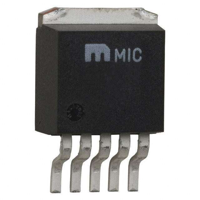
| 产品图片 | |
| 产品型号 | RT8580GE |
| PWM类型 | 电流模式 |
| rohs | 无铅 / 符合限制有害物质指令(RoHS)规范要求 |
| 产品系列 | - |
| 供应商器件封装 | SOT-23-6 |
| 其它名称 | 1028-1304-1 |
| 包装 | 剪切带 (CT) |
| 同步整流器 | 无 |
| 安装类型 | 表面贴装 |
| 封装/外壳 | SOT-23-6 |
| 工作温度 | -40°C ~ 85°C |
| 标准包装 | 1 |
| 电压-输入 | 3 V ~ 5.5 V |
| 电压-输出 | 3 V ~ 40 V |
| 电流-输出 | 500mA |
| 类型 | 升压(升压) |
| 输出数 | 1 |
| 输出类型 | 可调式 |
| 频率-开关 | 500kHz |


- 商务部:美国ITC正式对集成电路等产品启动337调查
- 曝三星4nm工艺存在良率问题 高通将骁龙8 Gen1或转产台积电
- 太阳诱电将投资9.5亿元在常州建新厂生产MLCC 预计2023年完工
- 英特尔发布欧洲新工厂建设计划 深化IDM 2.0 战略
- 台积电先进制程称霸业界 有大客户加持明年业绩稳了
- 达到5530亿美元!SIA预计今年全球半导体销售额将创下新高
- 英特尔拟将自动驾驶子公司Mobileye上市 估值或超500亿美元
- 三星加码芯片和SET,合并消费电子和移动部门,撤换高东真等 CEO
- 三星电子宣布重大人事变动 还合并消费电子和移动部门
- 海关总署:前11个月进口集成电路产品价值2.52万亿元 增长14.8%


PDF Datasheet 数据手册内容提取
® RT8580 36V DC-DC Boost Converter General Description Features The RT8580 is a high performance, low noise, DC-DC Boost Input Operating Range : 3V to 5.5V Converter with an integrated 0.5A, 1Ω internal switch. The Wide Output Range : VCC to 40V RT8580's input voltage ranges from 3V to 5.5V, and it can Internal Power N-MOSFET Switch support the output voltage up to 40V. When used in optical 500kHz Fixed Switching Frequency receiver applications requiring 80V to drive the APD Minimize the External Component Counts (Avalanche Photo Diode), the output voltage of the RT8580 Internal Soft-Start can be doubled up by a typical voltage doubler circuit. Internal Compensation The RT8580 adapts fixed frequency, current mode PWM Under-Voltage Lockout Protection control loop to regulate the output voltage with fast transient Over-Temperature Protection response and cycle-by-cycle current limit protection. The RoHS Compliant and Halogen Free protection features of the RT8580 include : 1) input under- Applications voltage lockout, 2) output over-voltage protection, and 3) over-temperature protection. The soft-start function and Cellular Phones PWM loop compensation is built-in internally to save Digital Cameras external soft-start capacitor and PWM loop compensation Portable Instruments components. By operating at 500kHz switching frequency, Avalanche Photodiode Biasing the RT8580 system board can be made compact to achieve low system BOM cost. The RT8580 is available in the Ordering Information tiny package type SOT-23-6. RT8580 Package Type Marking Information E : SOT-23-6 Lead Plating System 0E= : Product Code G : Green (Halogen Free and Pb Free) 0E=DNN DNN : Date Code Note : Richtek products are : RoHS compliant and compatible with the current require- ments of IPC/JEDEC J-STD-020. Suitable for use in SnPb or Pb-free soldering processes. Simplified Application Circuit L1 D1 VIN VOUT C1 RT8580 R1 VCC LX C2 SHDN FB GND R2 PGND Copyright © 2017 Richtek Technology Corporation. All rights reserved. is a registered trademark of Richtek Technology Corporation. DS8580-01 January 2017 www.richtek.com 1
RT8580 Pin Configuration (TOP VIEW) LX VCCSHDN 6 5 4 2 3 PGNDGND FB SOT-23-6 Functional Pin Description Pin No. Pin Name Pin Function 1 PGND Power ground. 2 GND Ground. 3 FB Feedback voltage input. Connect a resistor to GND to setting the current. Shutdown control input. Apply a logic-low voltage to SHDN to shut down the 4 SHDN device. Connect SHDN to VIN for normal operation. Ensure that SHDN is not greater than the input voltage, VCC. 5 VCC Supply voltage input. 6 LX Switch node. Functional Block Diagram VCC GND LX UVLO OCP Internal Compensation OTP Logic Control, Minimum On Current- Internal -PWM Time Sense Soft-Start + + Driver EA PGND GM Slope - + Compensation Shutdown PWM Enable Oscillator LPF 20ms Logic Reference VREF Voltage 1µA Bias Current FB SHDN Copyright © 2017 Richtek Technology Corporation. All rights reserved. is a registered trademark of Richtek Technology Corporation. www.richtek.com DS8580-01 January 2017 2
RT8580 Operation The RT8580 is a constant frequency, current mode Boost When the RT8580 is enabled by SHDN pin, the internal regulator. In normal operation, the N-MOSFET is turned V ramps up to the target voltage in a specific time REF on when the PWM control circuit is set by the oscillator. period. There is also a built-in soft-start function. Both As the N-MOSFET is on, the inductor current ramps up. ensure that the output voltage rises slowly to reduce the The N-MOSFET will be turned off when the inductor current input inrush current. hits the level set by the PWM control loop. After the The protection features of the RT8580 include : 1) input N-MOSFET is turned off, the inductor current will ramp under-voltage lockout, 2) output over-voltage protection, down through the external catch diode until the OSC sets and 3) over-temperature protection. When the input voltage high for the next switching cycle and the next cycle is lower than the UVLO threshold, the RT8580 will be repeats. turned off. There is a 100mV hysteresis for the UVLO The operation of the RT8580 can be better understood by control. When the junction temperature exceeds 150°C, referring to the block diagram. The voltage at the output of the over-temperature protection function will shut down the error amplifier is an amplified version of the difference the switching operation. Once the junction temperature between the 1.25V reference voltage and the output cools down by approximately 25°C, the converter will feedback voltage. If the feedback voltage drops below automatically resume switching. (above) 1.25V, the output of the error amplifier increases (decreases). This results in higher (lower) PWM turn on duty and thus higher (lower) inductor peak current flowing through the power FET. By this control loop operation, the increased (decreased) power will be delivered to the output to bring up (down) the output feedback voltage back to 1.25V. Copyright © 2017 Richtek Technology Corporation. All rights reserved. is a registered trademark of Richtek Technology Corporation. DS8580-01 January 2017 www.richtek.com 3
RT8580 Absolute Maximum Ratings (Note 1) VCC, SHDN,FB to GND-------------------------------------------------------------------------------------------------- −0.3V to 6V LX to GND -------------------------------------------------------------------------------------------------------------------- −0.3V to 50V Power Dissipation, P @ T = 25°C D A SOT-23-6 --------------------------------------------------------------------------------------------------------------------- 0.48W Package Thermal Resistance (Note 2) SOT-23-6, θ ---------------------------------------------------------------------------------------------------------------- 208.2°C/W JA Junction Temperature------------------------------------------------------------------------------------------------------ 150°C Lead Temperature (Soldering, 10 sec.)-------------------------------------------------------------------------------- 260°C Storage Temperature Range --------------------------------------------------------------------------------------------- −65°C to 150°C ESD Susceptibility (Note 3) HBM (Human Body Model)----------------------------------------------------------------------------------------------- 2kV MM (Machine Model) ------------------------------------------------------------------------------------------------------ 200V Recommended Operating Conditions (Note 4) Input Voltage, VCC--------------------------------------------------------------------------------------------------------- 3V to 5.5V Junction Temperature Range--------------------------------------------------------------------------------------------- −40°C to 125°C Ambient Temperature Range--------------------------------------------------------------------------------------------- −40°C to 85°C Electrical Characteristics (VCC = 3.3V, TA = 25°C, unless otherwise specified) Parameter Symbol Test Conditions Min Typ Max Unit Overall Under-Voltage Lockout Threshold VUVLO -- 2 2.4 V VCC Quiescent Current IQ 0.6 0.8 1.2 mA VCC Shutdown Current SHDN = 0V -- 2 5 A Shutdown Input Current ISHDN -- -- 2 A SHDN Threshold Logic-High VIH 1.4 -- -- V Voltage Logic-Low VIL -- -- 0.5 Oscillator Switching Frequency fSW 450 500 550 kHz Maximum Duty in Steady State DMAX 91 93 97 % Operation Line Regulation VCC = 3.3V to 4.3V 1.5 -- 1.5 % Feedback Reference Voltage 1.22 1.25 1.28 V Feedback Input Current IFB VFB = VFB_SET -- 100 500 nA LX On-Resistance RDS(ON) -- 0.7 1 LX Leakage Current VLX = 40V -- -- 4 A Switch Current Limit ILIM -- 330 -- mA Copyright © 2017 Richtek Technology Corporation. All rights reserved. is a registered trademark of Richtek Technology Corporation. www.richtek.com DS8580-01 January 2017 4
RT8580 Parameter Symbol Test Conditions Min Typ Max Unit Thermal Protection Thermal Shutdown Temperature TSD -- 150 -- C Thermal Shutdown Hysteresis T -- 25 -- C SD Note 1. Stresses beyond those listed “Absolute Maximum Ratings” may cause permanent damage to the device. These are stress ratings only, and functional operation of the device at these or any other conditions beyond those indicated in the operational sections of the specifications is not implied. Exposure to absolute maximum rating conditions may affect device reliability. Note 2. θJA is measured under natural convection (still air) at TA= 25°C with the component mounted on a high effective- thermal-conductivity four-layer test board on a JEDEC 51-7 thermal measurement standard. Note 3. Devices are ESD sensitive. Handling precaution is recommended. Note 4. The device is not guaranteed to function outside its operating conditions. Copyright © 2017 Richtek Technology Corporation. All rights reserved. is a registered trademark of Richtek Technology Corporation. DS8580-01 January 2017 www.richtek.com 5
RT8580 Typical Application Circuit L1 D1 VIN VOUT 3V to 5.5V 30V C1 2.2µF RT8580 R1 5 6 150k VCC LX C2 4 SHDN FB 3 4.7µF 2 GND R2 1 6.2k PGND Copyright © 2017 Richtek Technology Corporation. All rights reserved. is a registered trademark of Richtek Technology Corporation. www.richtek.com DS8580-01 January 2017 6
RT8580 Typical Operating Characteristics Efficiency vs. Load Current Quiescent Current vs. Input Voltage 100 1000 90 950 80 A) µ 900 %) 70 ent ( 850 Efficiency ( 456000 VVVIIINNN === 543...583VVV scent Curr 785000 30 e ui 700 20 Q 650 10 VOUT = 30V Device Not Switching 0 600 0 0.5 1 1.5 2 2.5 3 3.5 4 2 2.5 3 3.5 4 4.5 5 5.5 6 Load Current (mA) Input Voltage (V) No Load Quiescent Current vs. Input Voltage Quiescent Current vs. Temperature 16 900 1 A) m 14 VIN = 5V nt ( A) 850 e 12 µ urr nt ( 800 C 10 e nt urr e 8 C 750 sc nt e e Qui 6 sc 700 VIN = 3V d 4 uie a Q o L 650 o 2 N VOUT = 30V Device Not Switching 0 600 2.5 3 3.5 4 4.5 5 5.5 -50 -25 0 25 50 75 100 125 Input Voltage (V) Temperature (°C) Switching Frequency vs. Temperature Feedback Voltage vs. Temperature 520 1.30 1 515 z) H 510 1.28 cy (k 505 e (V) n g e 500 a1.26 qu olt e 495 V Fr k VIN = 5V g 490 ac1.24 VIN = 3V n b hi 485 d c e wit 480 Fe1.22 S 475 VIN = 5V, VOUT = 30V 470 1.20 -50 -25 0 25 50 75 100 125 -50 -25 0 25 50 75 100 125 Temperature (°C) Temperature (°C) Copyright © 2017 Richtek Technology Corporation. All rights reserved. is a registered trademark of Richtek Technology Corporation. DS8580-01 January 2017 www.richtek.com 7
RT8580 Light Load Switching Heavy Load Switching VOUT_ac VOUT_ac (2mV/Div) (2mV/Div) LX LX (20V/Div) (20V/Div) IL IL (100mA/Div) (100mA/Div) VIN = 5V, VOUT = 30V, IOUT = 0.1mA VIN = 5V, VOUT = 30V, IOUT = 4mA Time (1μs/Div) Time (1μs/Div) Power On from SHDN Power Off from SHDN VOUT VOUT (20V/Div) (20V/Div) SHDN SHDN (5V/Div) (5V/Div) IL IL (100mA/Div) (100mA/Div) VIN = 5V, VOUT = 30V, IOUT = 2mA VIN = 5V, VOUT = 30V, IOUT = 2mA Time (10ms/Div) Time (50ms/Div) Load Transient Response VOUT_ac (100mV/Div) IOUT (2mA/Div) VIN = 5V, VOUT = 30V, IOUT = 0 to 4mA Time (1ms/Div) Copyright © 2017 Richtek Technology Corporation. All rights reserved. is a registered trademark of Richtek Technology Corporation. www.richtek.com DS8580-01 January 2017 8
RT8580 Application Information The RT8580 current-mode PWM controllers operate in should have a current rating greater than the current-limit wide range of DC-DC conversion applications for boost. value. The inductor saturation current rating should be This converter provides low noise, high output voltages. considered to cover the inductor peak current. Other features include shutdown, fixed 500kHz PWM Soft-Start oscillator, and a input range : 3V to 5.5V for the RT8580. The function of soft-start is made for suppressing the inrush The RT8580 operates in discontinuous mode in order to current to an acceptable value at the beginning of power reduce the switching noise at the output. Other continuous on. The RT8580 provides a built-in soft-start function by mode Boost converters generate a large voltage spike at clamping the output voltage of error amplifier so that the the output when the LX switch turns on because there is duty cycle of the PWM will be increased gradually in the a conduction path between the output, diode, and switch soft-start period. to ground during the time needed for the diode to turn off. Current Limiting SHDN Input The current flow through inductor as charging period is The SHDN pin provides shutdown control. Connect SHDN detected by a current sensing circuit. As the value comes to VCC for normal operation. To disable the device, connect across the current limiting threshold, the N-MOSFET will SHDN to GND. be turned off so that the inductor will be forced to leave Constant Output Voltage Control charging stage and enter discharging stage. Therefore, the inductor current will not increase over the current The output voltage of the RT8580 is fixed at 30V. The limiting threshold. output voltage is set by two external resistors (R1 and R2). First select the value of R2 in the 5kΩ to 50kΩ range. Diode Selection R1 is then given by : The RT8580's high switching frequency demands a high- V R1R2 OUT 1 speed rectifier. Schottky diodes are recommended for VREF most applications because of their fast recovery time and where V is 1.25V REF low forward-voltage drop. Ensure that the diode's peak current rating is greater than or equal to the peak inductor Determining Peak Inductor Current current. Also, the diode reverse breakdown voltage must If the Boost converter remains in the discontinuous mode be greater than V . of operation, then the approximate peak inductor current, OUT I , is represented by the formula below : LPEAK Input Capacitor Selection 2T (V V )I I S OUT IN OUT Low ESR ceramic capacitors are recommended for input LPEAK L capacitor applications. Low ESR will effectively reduce where TS is the period, VOUT is the output voltage, VIN is the input voltage ripple caused by switching operation. A the input voltage, IOUT is the output current, and η is the 4.7μF capacitor is sufficient for most applications. efficiency of the boost converter. Nevertheless, this value can be decreased for lower output current requirement. Another consideration is the voltage Inductor Selection rating of the input capacitor which must be greater than The recommended value of inductor for 30V, 22μH is the the maximum input voltage. recommended inductor value when the output voltage is 30V and the input voltage is 5V. In general, the inductor Copyright © 2017 Richtek Technology Corporation. All rights reserved. is a registered trademark of Richtek Technology Corporation. DS8580-01 January 2017 www.richtek.com 9
RT8580 Over-Temperature Protection 0.6 The RT8580 has Over-Temperature Protection (OTP) W) 1 Four-Layer PCB function to prevent the excessive power dissipation from n ( 0.5 o overheating. The OTP function will shut down switching ati p 0.4 operation when the die junction temperature exceeds si s 150°C. The chip will automatically start to switch again r Di 0.3 e when the die junction temperature cools off. w o P 0.2 m Thermal Considerations u m 0.1 The junction temperature should never exceed the xi a M absolute maximum junction temperature TJ(MAX), listed 0.0 under Absolute Maximum Ratings, to avoid permanent 0 25 50 75 100 125 damage to the device. The maximum allowable power Ambient Temperature (°C) dissipation depends on the thermal resistance of the IC Figure 1. Derating Curve of Maximum Power Dissipation package, the PCB layout, the rate of surrounding airflow, and the difference between the junction and ambient Layout Considerations temperatures. The maximum power dissipation can be PCB layout is very important when designing power calculated using the following formula : switching converter circuits. Some recommended layout P = (T − T ) / θ guide lines are as follows : D(MAX) J(MAX) A JA The power components L1, D1 and C2 must be placed as where T is the maximum junction temperature, T is J(MAX) A the ambient temperature, and θ is the junction-to-ambient close to each other as possible to reduce the ac current JA loop area. The PCB trace between power components thermal resistance. must be as short and wide as possible due to large current For continuous operation, the maximum operating junction flow through these traces during operation. temperature indicated under Recommended Operating Conditions is 125°C. The junction-to-ambient thermal Place L1 and D1 as close to the LX Pin as possible. The resistance, θ , is highly package dependent. For a SOT- trace should be as short and wide as possible. JA 23-6, the thermal resistance, θJA, is 208.2°C/W on a The input capacitor C1 must be placed as close to the standard JEDEC 51-7 high effective-thermal-conductivity VCC pin as possible. four-layer test board. The maximum power dissipation at Place these components as Locate input capacitor as TA = 25°C can be calculated as below : close as possible to the LX Pin. close to VCC as possible. P = (125°C − 25°C) / (208.2°C/W) = 0.48W for a C1 D(MAX) VIN SOT-23-6 package. L1 D1 The maximum power dissipation depends on the operating LX VCCSHDN ambient temperature for the fixed T and the thermal J(MAX) resistance, θ . The derating curves in Figure 1 allows 6 5 4 JA GND the designer to see the effect of rising ambient temperature 2 3 on the maximum power dissipation. PGNDGND FB R1 R2 C2 VOUT Figure 2. PCB Layout Guide Copyright © 2017 Richtek Technology Corporation. All rights reserved. is a registered trademark of Richtek Technology Corporation. www.richtek.com DS8580-01 January 2017 10
RT8580 Outline Dimension H D L C B b A A1 e Dimensions In Millimeters Dimensions In Inches Symbol Min Max Min Max A 0.889 1.295 0.031 0.051 A1 0.000 0.152 0.000 0.006 B 1.397 1.803 0.055 0.071 b 0.250 0.560 0.010 0.022 C 2.591 2.997 0.102 0.118 D 2.692 3.099 0.106 0.122 e 0.838 1.041 0.033 0.041 H 0.080 0.254 0.003 0.010 L 0.300 0.610 0.012 0.024 SOT-23-6 Surface Mount Package Richtek Technology Corporation 14F, No. 8, Tai Yuen 1st Street, Chupei City Hsinchu, Taiwan, R.O.C. Tel: (8863)5526789 Richtek products are sold by description only. Richtek reserves the right to change the circuitry and/or specifications without notice at any time. Customers should obtain the latest relevant information and data sheets before placing orders and should verify that such information is current and complete. Richtek cannot assume responsibility for use of any circuitry other than circuitry entirely embodied in a Richtek product. Information furnished by Richtek is believed to be accurate and reliable. However, no responsibility is assumed by Richtek or its subsidiaries for its use; nor for any infringements of patents or other rights of third parties which may result from its use. No license is granted by implication or otherwise under any patent or patent rights of Richtek or its subsidiaries. DS8580-01 January 2017 www.richtek.com 11