ICGOO在线商城 > 集成电路(IC) > PMIC - 稳压器 - DC DC 开关稳压器 > RT8297AZQW
 Datasheet下载
- 型号: RT8297AZQW
- 制造商: RICHTEK
- 库位|库存: xxxx|xxxx
- 要求:
| 数量阶梯 | 香港交货 | 国内含税 |
| +xxxx | $xxxx | ¥xxxx |
查看当月历史价格
查看今年历史价格
RT8297AZQW产品简介:
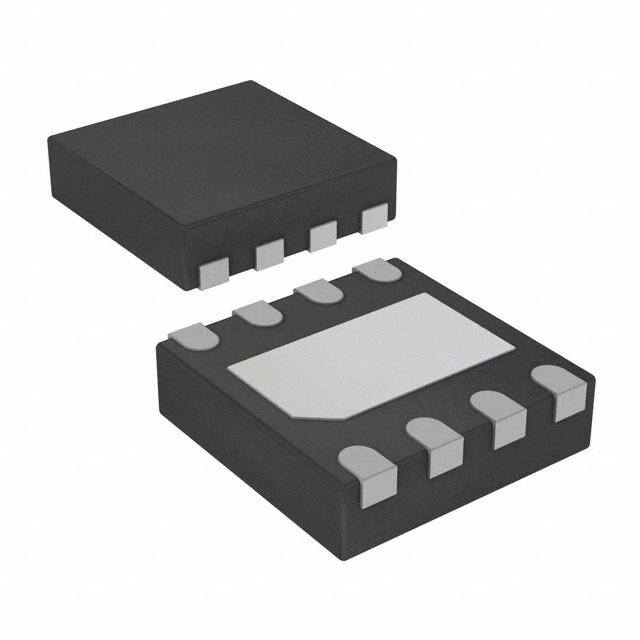
ICGOO电子元器件商城为您提供RT8297AZQW由RICHTEK设计生产,在icgoo商城现货销售,并且可以通过原厂、代理商等渠道进行代购。 RT8297AZQW价格参考。RICHTEKRT8297AZQW封装/规格:PMIC - 稳压器 - DC DC 开关稳压器, 可调式 降压 开关稳压器 IC 正 0.8V 1 输出 1.5A 8-WFDFN 裸露焊盘。您可以下载RT8297AZQW参考资料、Datasheet数据手册功能说明书,资料中有RT8297AZQW 详细功能的应用电路图电压和使用方法及教程。
| 参数 | 数值 |
| 产品目录 | 集成电路 (IC) |
| 描述 | IC REG BUCK SYNC ADJ 1.5A 8WDFN |
| 产品分类 | |
| 品牌 | Richtek USA Inc |
| 数据手册 | http://www.richtek.com/download_ds.jsp?s=679 |
| 产品图片 | |
| 产品型号 | RT8297AZQW |
| PWM类型 | 电流模式 |
| rohs | 无铅 / 符合限制有害物质指令(RoHS)规范要求 |
| RoHS指令信息 | http://www.richtek.com/download.jsp?t=UyUyRmFzc2V0cyUyRjIwMDklMkYwNiUyRjE3JTJGcGFnZTY1MTYwenRpeGIucGRmJTNEJTNEJTNE%0AR0w5NTI1LUMtLVBiLWZyZWUrUHJvZHVjdCsrR3JlZW4rUHJvZHVjdCtTdGF0ZW1lbnQrMDkwNjE2%0AQw%3D%3D |
| 产品系列 | - |
| 供应商器件封装 | 8-WDFN(2x2) |
| 其它名称 | 1028-1154-6 |
| 包装 | Digi-Reel® |
| 同步整流器 | 是 |
| 安装类型 | 表面贴装 |
| 封装/外壳 | 8-WFDFN 裸露焊盘 |
| 工作温度 | -40°C ~ 85°C |
| 标准包装 | 1 |
| 电压-输入 | 4 V ~ 17 V |
| 电压-输出 | 0.8 V ~ 12 V |
| 电流-输出 | 1.5A |
| 类型 | 降压(降压) |
| 输出数 | 1 |
| 输出类型 | 可调式 |
| 频率-开关 | 340kHz |


- 商务部:美国ITC正式对集成电路等产品启动337调查
- 曝三星4nm工艺存在良率问题 高通将骁龙8 Gen1或转产台积电
- 太阳诱电将投资9.5亿元在常州建新厂生产MLCC 预计2023年完工
- 英特尔发布欧洲新工厂建设计划 深化IDM 2.0 战略
- 台积电先进制程称霸业界 有大客户加持明年业绩稳了
- 达到5530亿美元!SIA预计今年全球半导体销售额将创下新高
- 英特尔拟将自动驾驶子公司Mobileye上市 估值或超500亿美元
- 三星加码芯片和SET,合并消费电子和移动部门,撤换高东真等 CEO
- 三星电子宣布重大人事变动 还合并消费电子和移动部门
- 海关总署:前11个月进口集成电路产品价值2.52万亿元 增长14.8%


PDF Datasheet 数据手册内容提取
® RT8297A/B 1.5A, 17V, 340/800kHz Synchronous Step-Down Converter General Description Features The RT8297A/B is a high efficiency, monolithic (cid:122)(cid:122)(cid:122)(cid:122)(cid:122) 4V to 17V Input Voltage Range synchronous step-down DC/DC converter that can operate (cid:122)(cid:122)(cid:122)(cid:122)(cid:122) 1.5A Output Current at 340kHz/800kHz, while delivering up to 1.5A output (cid:122)(cid:122)(cid:122)(cid:122)(cid:122) Internal N-MOSFETs current from a 4V to 17V input supply. The RT8297A/B's (cid:122)(cid:122)(cid:122)(cid:122)(cid:122) Current Mode Control current mode architecture allows the transient response (cid:122)(cid:122)(cid:122)(cid:122)(cid:122) Fixed Frequency Operation : 340kHz/800kHz to be optimized. Cycle-by-cycle current limit provides (cid:122)(cid:122)(cid:122)(cid:122)(cid:122) Output Adjustable from 0.8V to 12V protection against shorted outputs and soft-start eliminates (cid:122)(cid:122)(cid:122)(cid:122)(cid:122) Up to 95% Efficiency input current surge during start-up. Fault conditions also (cid:122)(cid:122)(cid:122)(cid:122)(cid:122) Internal Compensation include output under voltage protection, output over voltage (cid:122)(cid:122)(cid:122)(cid:122)(cid:122) Stable with Low ESR Ceramic Output Capacitors protection, and thermal shutdown. The low current (<5μA) (cid:122)(cid:122)(cid:122)(cid:122)(cid:122) Cycle-by-Cycle Over Current Protection shutdown mode provides output disconnect, enabling easy (cid:122)(cid:122)(cid:122)(cid:122)(cid:122) Input Under Voltage Lockout power management in battery-powered systems. The (cid:122)(cid:122)(cid:122)(cid:122)(cid:122) Output Under Voltage Protection RT8297A/B is available in a WDFN-8L 2x2 package. (cid:122)(cid:122)(cid:122)(cid:122)(cid:122) Output Over Voltage Protection Power Good Indicator (cid:122)(cid:122)(cid:122)(cid:122)(cid:122) Ordering Information Thermal Shutdown Protection (cid:122)(cid:122)(cid:122)(cid:122)(cid:122) RT8297A/B (cid:122)(cid:122)(cid:122)(cid:122)(cid:122) RoHS Compliant and Halogen Free Package Type Applications QW : WDFN-8L 2x2 (W-Type) Lead Plating System (cid:122)(cid:122)(cid:122)(cid:122)(cid:122) Industrial and Commercial Low Power Systems Z : ECO (Ecological Element with Computer Peripherals (cid:122)(cid:122)(cid:122)(cid:122)(cid:122) Halogen Free and Pb free) LCD Monitors and TVs (cid:122)(cid:122)(cid:122)(cid:122)(cid:122) A : 340kHz Green Electronics/Appliances (cid:122)(cid:122)(cid:122)(cid:122)(cid:122) B : 800kHz Point of Load Regulation for High-Performance DSPs, (cid:122)(cid:122)(cid:122)(cid:122)(cid:122) Note : FPGAs, and ASICs Richtek products are : (cid:96) RoHS compliant and compatible with the current require- Pin Configurations ments of IPC/JEDEC J-STD-020. (cid:96) Suitable for use in SnPb or Pb-free soldering processes. (TOP VIEW) SW 1 8 GND Marking Information VIN 2 ND 7 GND BOOT 3 G 6 PGOOD RT8297AZQW EN 4 9 5 FB 00 : Product Code WDFN-8L 2x2 00W W : Date Code RT8297BZQW 71 : Product Code 71W W : Date Code Copyright © 2013 Richtek Technology Corporation. All rights reserved. is a registered trademark of Richtek Technology Corporation. DS8297A/B-06 June 2013 www.richtek.com 1
RT8297A/B Typical Application Circuit RT8297A VIN 2 VIN BOOT 3 4V to 17V CIN CBOOT 10µF 10nF L 1 15µH VOUT SW 3.3V 6 PGOOD PGOOD 1.5A R1 Chip Enable FB 5 110k 4 EN R2 COUT 36k 22µF x 2 7, 8, 9 (Exposed Pad) GND RT8297B VIN 2 VIN BOOT 3 4V to 17V CIN CBOOT 10µF 10nF L 1 6.8µH VOUT SW 3.3V 6 PGOOD PGOOD 1.5A R1 Chip Enable FB 5 47k 4 EN R2 COUT 15k 22µF x 2 7, 8, 9 (Exposed Pad) GND Table 1. Recommended Component Selection RT8297A VOUT (V) L (μH) R1 (kΩ) R2 (kΩ) COUT (μF) 1.2 4.7 110 220 22 x 2 2.5 10 110 51 22 x 2 3.3 15 110 36 22 x 2 5 22 120 22 22 x 2 RT8297B V (V) L (μH) R1 (kΩ) R2 (kΩ) C (μF) OUT OUT 1.2 3.6 47 91 22 x 2 2.5 4.7 47 22 22 x 2 3.3 6.8 47 15 22 x 2 5 10 62 12 22 x 2 Copyright © 2013 Richtek Technology Corporation. All rights reserved. is a registered trademark of Richtek Technology Corporation. www.richtek.com DS8297A/B-06 June 2013 2
RT8297A/B Functional Pin Description Pin No. Pin Name Pin Function 1 SW Switch Node. Connect to external L-C filter. Input Supply Voltage. Must bypass with a suitably large ceramic 2 VIN capacitor. Bootstrap for High Side Gate Driver. Connect 0.01μF or greater ceramic 3 BOOT capacitor from BOOT to SW pin. Chip Enable. A logic-high enables the converter; a logic-low forces the RT8297A/B into shutdown mode, reducing the supply current to less 4 EN than 5μA. Attach this pin to VIN with a 100kΩ pull up resistor for automatic startup. Feedback Input Pin. For an adjustable output, connect an external 5 FB resistive voltage divider to this pin. Power Good Indicator. The output of this pin is low if the output voltage is 6 PGOOD 12.5% less than the nominal voltage. Otherwise, it is an open drain. Ground. The exposed pad must be soldered to a large PCB and 7, 8, 9 (Exposed Pad) GND connected to GND for maximum power dissipation. Function Block Diagram VIN Internal OSC Regulator 340kHz/800kHz Enable Comparator VA VCC Slope Comp + 2.5V + Foldback Current Sense - EN - Amplifier 5k Control 3V VA 1V + OV BOOT - OV Comparator S Q 145m + 0.4V + R Q UV - - Current SW Comparator UV Comparator 140m 0.8V + FB - Error Amp PGOOD GND Comparator 35pF 400k + 0.7V - FB 1pF PGOOD Copyright © 2013 Richtek Technology Corporation. All rights reserved. is a registered trademark of Richtek Technology Corporation. DS8297A/B-06 June 2013 www.richtek.com 3
RT8297A/B Absolute Maximum Ratings (Note 1) Supply Voltage, VIN ----------------------------------------------------------------------------------------- −0.3V to 19V (cid:122) SW--------------------------------------------------------------------------------------------------------------- −0.3V to (V + 0.3V) (cid:122) IN BOOT to SW -------------------------------------------------------------------------------------------------- −0.3V to 6V (cid:122) All Other Pins ------------------------------------------------------------------------------------------------- −0.3V to 6V (cid:122) Power Dissipation, P @ T = 25°C (cid:122) D A WDFN-8L 2x2 ------------------------------------------------------------------------------------------------- 0.833W Package Thermal Resistance (Note 2) (cid:122) WDFN-8L 2x2, θ -------------------------------------------------------------------------------------------- 120°C/W JA WDFN-8L 2x2, θ -------------------------------------------------------------------------------------------- 8.2°C/W JC Lead Temperature (Soldering, 10 sec.)------------------------------------------------------------------ 260°C (cid:122) Junction Temperature---------------------------------------------------------------------------------------- 150°C (cid:122) Storage Temperature Range ------------------------------------------------------------------------------- −65°C to 150°C (cid:122) ESD Susceptibility (Note 3) (cid:122) HBM (Human Body Model)--------------------------------------------------------------------------------- 2kV MM (Machine Model) ---------------------------------------------------------------------------------------- 200V Recommended Operating Conditions (Note 4) Supply Input Voltage, VIN ---------------------------------------------------------------------------------- 4V to 17V (cid:122) Junction Temperature Range------------------------------------------------------------------------------- −40°C to 125°C (cid:122) Ambient Temperature Range------------------------------------------------------------------------------- −40°C to 85°C (cid:122) Electrical Characteristics (VIN = 12V, TA = 25°C, unless otherwise specified) Parameter Symbol Test Conditions Min Typ Max Unit Shutdown Supply Current I V = 0V -- 1 5 μA SHDN EN Supply Current IOUT VEN = 3V, VFB = 0.9V -- 0.6 1 mA Feedback Reference Voltage VREF 4V ≤ VIN ≤ 17V 0.788 0.800 0.812 V Feedback Current IFB VFB = 0.8V -- 10 -- nA High Side Switch On RDS(ON)1 -- 145 -- mΩ Resistance Low Side Switch On Resistance RDS(ON)2 -- 140 -- mΩ Min. Duty Cycle, VBOOT − VSW = 4.8V Upper Switch Current Limit 2.45 3 4.65 A Maximum Loading = 1.5A Lower Switch Current Limit From Drain to Source -- 1 -- A For RT8297A 300 340 380 Oscillation Frequency fOSC1 kHz For RT8297B 700 800 900 Short-Circuit Oscillation VFB = 0V, For RT8297A -- 95 -- fOSC2 kHz Frequency V = 0V, For RT8297B -- 170 -- FB V = 0.7V, For RT8297A -- 93 -- % FB Maximum Duty Cycle DMAX VFB = 0.7V, For RT8297B -- 84 -- % Copyright © 2013 Richtek Technology Corporation. All rights reserved. is a registered trademark of Richtek Technology Corporation. www.richtek.com DS8297A/B-06 June 2013 4
RT8297A/B Parameter Symbol Test Conditions Min Typ Max Unit Minimum On-Time t -- 100 125 ns ON Input Under Voltage Lockout VUVLO -- 3.5 -- V Threshold Input Under Voltage Lockout Threshold Hysteresis ΔVUVLO -- 200 -- mV EN Threshold Logic-High VIH 2.5 -- -- V Voltage Logic-Low VIL -- -- 0.4 EN Pull Low Current VEN = 2V, VFB = 1V -- 1 -- μA Soft-Start Period tSS -- 1 -- ms Thermal Shutdown T -- 150 -- °C SD Thermal Shutdown ΔT -- 15 -- °C Hysteresis SD Power Good Threshold -- 0.7 -- V Rising Power Good Threshold -- 130 -- mV Hysteresis Power Good Pull Down -- 12 -- Ω Resistance Output OVP Trip Threshold -- 125 -- %VREF Output OVP Prop Delay -- 10 -- μs Output UVP Trip Threshold -- 50 -- %VREF Output UVP Prop Delay -- 2 -- μs Note 1. Stresses beyond those listed “Absolute Maximum Ratings” may cause permanent damage to the device. These are stress ratings only, and functional operation of the device at these or any other conditions beyond those indicated in the operational sections of the specifications is not implied. Exposure to absolute maximum rating conditions may affect device reliability. Note 2. θJA is measured at TA= 25°C on a high effective thermal conductivity four-layer test board per JEDEC 51-7. θJC is measured at the exposed pad of the package. Note 3. Devices are ESD sensitive. Handling precaution is recommended. Note 4. The device is not guaranteed to function outside its operating conditions. Copyright © 2013 Richtek Technology Corporation. All rights reserved. is a registered trademark of Richtek Technology Corporation. DS8297A/B-06 June 2013 www.richtek.com 5
RT8297A/B Typical Operating Characteristics Efficiency vs. Output Current Efficiency vs. Output Current 100 100 90 90 80 80 %) 70 VVOOUUTT == 53V.3V %) 70 VOUT = 5V Efficiency ( 456000 VOUT = 1.2V Efficiency ( 456000 VVOOUUTT == 31..32VV 30 30 20 20 10 10 RT8297A, VIN = 12V RT8297B, VIN = 12V 0 0 0.01 0.10 1.00 10.00 0.01 0.10 1.00 10.00 Output Current (A) Output Current (A) Output Voltage vs. Output Current Output Voltage vs. Output Current 5.10 3.40 5.06 3.36 V) V) e ( e ( g 5.02 g 3.32 a a olt olt V V ut 4.98 ut 3.28 p p ut ut O O 4.94 3.24 RT8297A, VIN = 12V, VOUT = 5V RT8297B, VIN = 12V, VOUT = 3.3V 4.90 3.20 0.0 0.3 0.6 0.9 1.2 1.5 0.0 0.3 0.5 0.8 1.0 1.3 1.5 Output Current (A) Output Current (A) Reference Voltage vs. Temperature Reference Voltage vs. Temperature 1.00 1.00 0.95 0.95 V) 0.90 V) 0.90 e ( e ( ag 0.85 ag 0.85 olt olt V 0.80 V 0.80 e e enc 0.75 enc 0.75 er er ef 0.70 ef 0.70 R R 0.65 0.65 RT8297A, VIN = 12V, IOUT = 0A RT8297B, VIN = 12V, IOUT = 0A 0.60 0.60 -50 -25 0 25 50 75 100 125 -50 -25 0 25 50 75 100 125 Temperature (°C) Temperature (°C) Copyright © 2013 Richtek Technology Corporation. All rights reserved. is a registered trademark of Richtek Technology Corporation. www.richtek.com DS8297A/B-06 June 2013 6
RT8297A/B Frequency vs. Input Voltage Frequency vs. Input Voltage 355 860 350 850 345 Hz) 1 340 Hz) 1 840 y (k 335 y (k 830 c c 820 en 330 en u u q q 810 e 325 e Fr Fr 800 320 315 790 RT8297A, VOUT = 3.3V, IOUT = 0.3A RT8297B, VOUT = 3.3V, IOUT = 0.3A 310 780 4 6 8 10 12 14 16 18 4 6 8 10 12 14 16 18 Input Voltage (V) Input Voltage (V) Frequency vs. Temperature Frequency vs. Temperature 400 900 875 375 Hz) 1 350 Hz) 1 850 y (k y (k 825 nc 325 nc 800 e e u u q q 775 e 300 e Fr Fr 750 275 725 RT8297A, VOUT = 3.3V, IOUT = 0.3A RT8297B, VOUT = 3.3V, IOUT = 0.3A 250 700 -50 -25 0 25 50 75 100 125 -50 -25 0 25 50 75 100 125 Temperature (°C) Temperature (°C) Quiescent Current vs. Input Voltage Quiescent Current vs. Input Voltage 900 1000 950 850 A) A) μ μ 900 ent ( 800 ent ( 850 urr urr C 750 C 800 nt nt e e 750 sc 700 sc e e ui ui 700 Q Q 650 650 RT8297A, VEN = 3.3V, VFB = 0.85V RT8297B, VEN = 3.3V, VFB = 0.85V 600 600 4 6 8 10 12 14 16 18 4 6 8 10 12 14 16 18 Input Voltage (V) Input Voltage (V) Copyright © 2013 Richtek Technology Corporation. All rights reserved. is a registered trademark of Richtek Technology Corporation. DS8297A/B-06 June 2013 www.richtek.com 7
RT8297A/B Quiescent Current vs. Temperature Quiescent Current vs. Temperature 0.90 0.90 ) 0.85 ) 0.85 A A m m nt ( 0.80 nt ( 0.80 e e rr rr u u C 0.75 C 0.75 nt nt e e sc 0.70 sc 0.70 e e ui ui Q Q 0.65 0.65 RT8297A, VIN = 12V, VEN = 3.3V, VFB = 0.85V RT8297B, VIN = 12V, VEN = 3.3V, VFB = 0.85V 0.60 0.60 -50 -25 0 25 50 75 100 125 -50 -25 0 25 50 75 100 125 Temperature (°C) Temperature (°C) Current Limit vs. Input Voltage Current Limit vs. Input Voltage 3.8 4.0 RT8297A RT8297B 3.6 3.8 VOUT = 3.3V 3.4 3.6 A) 3.2 VOUT = 3.3V A) 3.4 VOUT = 1.2V mit ( mit ( 3.2 3.0 nt Li 2.8 VOUT = 1.2V nt Li 3.0 e e 2.8 rr rr u 2.6 u C C 2.6 2.4 2.4 2.2 2.2 2.0 2.0 4 6 8 10 12 14 16 18 4 6 8 10 12 14 16 18 Input Voltage (V) Input Voltage (V) Current Limit vs. Temperature Current Limit vs. Temperature 3.9 4.0 RT8297A RT8297B 3.6 3.7 3.3 1 ) mit (A) 3.0 Limit (A 3.4 ent Li 22..47 rrent 3.1 urr Cu C 2.1 2.8 1.8 VIN = 12V, VOUT = 1.2V VIN = 12V, VOUT = 1.2V 1.5 2.5 -50 -25 0 25 50 75 100 125 -50 -25 0 25 50 75 100 125 Temperature (°C) Temperature (°C) Copyright © 2013 Richtek Technology Corporation. All rights reserved. is a registered trademark of Richtek Technology Corporation. www.richtek.com DS8297A/B-06 June 2013 8
RT8297A/B Load Transient Response Load Transient Response RT8297A RT8297B VOUT VOUT (100mV/Div) (50mV/Div) IOUT IOUT (1A/Div) (1A/Div) VIN = 12V, VOUT = 3.3V, IOUT = 0.1A to 1.5A VIN = 12V, VOUT = 3.3V, IOUT = 0.1A to 1.5A Time (1ms/Div) Time (1ms/Div) Switching Switching RT8297A RT8297B VSW VSW (10V/Div) (10V/Div) VOUT VOUT (5mV/Div) (5mV/Div) IL IL (1A/Div) (1A/Div) VIN = 12V, VOUT = 3.3V, IOUT = 1.5A VIN = 12V, VOUT = 3.3V, IOUT = 1.5A Time (5μs/Div) Time (500ns/Div) Power On from EN Power On from EN RT8297A RT8297B, VIN = 12V, VOUT = 3.3V, IOUT = 1.5A VEN VEN (5V/Div) (5V/Div) PGOOD PGOOD (5V/Div) (5V/Div) VOUT VOUT (2V/Div) (2V/Div) IOUT IOUT (2A/Div) (2A/Div) VIN = 12V, VOUT = 3.3V, IOUT = 1.5A Time (500μs/Div) Time (500μs/Div) Copyright © 2013 Richtek Technology Corporation. All rights reserved. is a registered trademark of Richtek Technology Corporation. DS8297A/B-06 June 2013 www.richtek.com 9
RT8297A/B Power Off from EN Power Off from EN RT8297A RT8297B, VIN = 12V, VOUT = 3.3V, IOUT = 1.5A VEN VEN (5V/Div) (5V/Div) PGOOD PGOOD (5V/Div) (5V/Div) VOUT VOUT (2V/Div) (2V/Div) IOUT IOUT (2A/Div) (2A/Div) VIN = 12V, VOUT = 3.3V, IOUT = 1.5A Time (100μs/Div) Time (100μs/Div) Copyright © 2013 Richtek Technology Corporation. All rights reserved. is a registered trademark of Richtek Technology Corporation. www.richtek.com DS8297A/B-06 June 2013 10
RT8297A/B Application Information The RT8297A/B is a synchronous high voltage buck Thermal Shutdown converter that can support the input voltage range from Thermal shutdown is implemented to prevent the chip from 4V to 17V and the output current can be up to 1.5A. operating at excessively high temperatures. When the junction temperature is higher than 150°C, the whole chip Output Voltage Setting is shutdown. The chip is automatically re-enable when The resistive divider allows the FB pin to sense the output the junction temperature cools down by approximately voltage as shown in Figure 1. 15 degrees. VOUT Over Voltage Protection (OVP) R1 The RT8297A/B provides Over Voltage Protection function FB when output voltage over 125%. The internal MOS will be RT8297A/B R2 turned off. The control will return to normal operation if GND over voltage condition is removed. Figure 1. Output Voltage Setting Under Voltage Protection (UVP) The output voltage is set by an external resistive divider For the RT8297A/B, it provides Hiccup Mode Under according to the following equation : Voltage Protection (UVP). When the FB voltage drops ⎛ R1⎞ below 50% of the feedback reference voltage, the UVP VOUT = VREF⎜1+ ⎟ ⎝ R2⎠ function will be triggered and the RT8297A/B will shut down Where V is the feedback reference voltage (0.8V typ.). for a period of time and then recover automatically. The REF Hiccup Mode UVP can reduce input current in short-circuit External Bootstrap Diode conditions. Connect a 10nF low ESR ceramic capacitor between the Inductor Selection BOOT pin and SW pin. This capacitor provides the gate driver voltage for the high side MOSFET. It is recommended The inductor value and operating frequency determine the to add an external bootstrap diode between an external ripple current according to a specific input and output 5V and the BOOT pin for efficiency improvement when voltage. The ripple current ΔIL increases with higher VIN input voltage is lower than 5.5V or duty ratio is higher and decreases with higher inductance. than 65%. The bootstrap diode can be a low cost one ΔIL = ⎡⎢VOUT⎤⎥⎡⎢1−VOUT⎤⎥ such as 1N4148 or BAT54. The external 5V can be a 5V ⎣ f×L ⎦⎣ VIN ⎦ fixed input from system or a 5V output of the RT8297A/B. Having a lower ripple current reduces not only the ESR Note that the external boot voltage must be lower than losses in the output capacitors but also the output voltage 5.5V ripple. High frequency with small ripple current can achieve highest efficiency operation. However, it requires a large 5V inductor to achieve this goal. For the ripple current selection, the value of ΔI = 0.2(I ) will be a reasonable L MAX BOOT starting point. The largest ripple current occurs at the RT8297A/B 10nF highest VIN. To guarantee that the ripple current stays SW below the specified maximum, the inductor value should be chosen according to the following equation : Figure 2. External Bootstrap Diode ⎡ V ⎤⎡ V ⎤ L = ⎢ OUT ⎥⎢1− OUT ⎥ ⎢⎣f×ΔIL(MAX)⎥⎦⎢⎣ VIN(MAX)⎥⎦ Copyright © 2013 Richtek Technology Corporation. All rights reserved. is a registered trademark of Richtek Technology Corporation. DS8297A/B-06 June 2013 www.richtek.com 11
RT8297A/B Table 2. Suggested Inductors for Typical types. Although Tantalum capacitors have the highest Application Circuit capacitance density, it is important to only use types that Component Dimensions pass the surge test for use in switching power supplies. Series Supplier (mm) Aluminum electrolytic capacitors have significantly higher TDK VLF10045 10 x 9.7 x 4.5 ESR. However, it can be used in cost-sensitive applications TDK SLF12565 12.5 x 12.5 x 6.5 for ripple current rating and long term reliability TAIYO NR8040 8 x 8 x 4 considerations. Ceramic capacitors have excellent low YUDEN ESR characteristics but can have a high voltage coefficient and audible piezoelectric effects. The high Q of ceramic C and C Selection IN OUT capacitors with trace inductance can also lead to significant The input capacitance, CIN, is needed to filter the ringing. trapezoidal current at the source of the high side MOSFET. Higher values, lower cost ceramic capacitors are now To prevent large ripple current, a low ESR input capacitor becoming available in smaller case sizes. Their high ripple sized for the maximum RMS current should be used. The current, high voltage rating and low ESR make them ideal RMS current is given by : for switching regulator applications. However, care must IRMS = IOUT(MAX) VOUT VIN −1 be taken when these capacitors are used at input and VIN VOUT output. When a ceramic capacitor is used at the input This formula has a maximum at V = 2V , where I = and the power is supplied by a wall adapter through long IN OUT RMS I /2. This simple worst-case condition is commonly used wires, a load step at the output can induce ringing at the OUT for design because even significant deviations do not offer input, VIN. At best, this ringing can couple to the output much relief. Choose a capacitor rated at a higher and be mistaken as loop instability. At worst, a sudden temperature than required. Several capacitors may also inrush of current through the long wires can potentially be paralleled to meet size or height requirements in the cause a voltage spike at VIN large enough to damage the design. For the input capacitor, a 10μF low ESR ceramic part. capacitor is recommended. For the recommended Checking Transient Response capacitor, please refer to table 3 for more detail. The The regulator loop response can be checked by looking selection of C is determined by the required ESR to OUT at the load transient response. Switching regulators take minimize voltage ripple. Moreover, the amount of bulk several cycles to respond to a step in load current. When capacitance is also a key for C selection to ensure OUT a load step occurs, V immediately shifts by an amount that the control loop is stable. Loop stability can be OUT equal to ΔI (ESR) also begins to charge or discharge checked by viewing the load transient response as LOAD described in a later section. The output ripple, ΔV , is COUT generating a feedback error signal for the regulator OUT to return V to its steady-state value. During this determined by : OUT recovery time, V can be monitored for overshoot or ⎡ 1 ⎤ OUT ΔVOUT ≤ΔIL⎢⎣ESR+8fCOUT⎥⎦ ringing that would indicate a stability problem. The output ripple will be highest at the maximum input Thermal Considerations voltage since ΔI increases with input voltage. Multiple L For continuous operation, do not exceed absolute capacitors placed in parallel may be needed to meet the maximum junction temperature. The maximum power ESR and RMS current handling requirement. Dry tantalum, dissipation depends on the thermal resistance of the IC special polymer, aluminum electrolytic and ceramic package, PCB layout, rate of surrounding airflow, and capacitors are all available in surface mount packages. difference between junction and ambient temperature. The Special polymer capacitors offer very low ESR value. maximum power dissipation can be calculated by the However, it provides lower capacitance density than other following formula : Copyright © 2013 Richtek Technology Corporation. All rights reserved. is a registered trademark of Richtek Technology Corporation. www.richtek.com DS8297A/B-06 June 2013 12
RT8297A/B P = (T − T ) / θ Layout Consideration D(MAX) J(MAX) A JA where T is the maximum junction temperature, T is Follow the PCB layout guidelines for optimal performance J(MAX) A the ambient temperature, and θ is the junction to ambient of the RT8297A/B JA thermal resistance. (cid:96) Keep the traces of the main current paths as short and For recommended operating condition specifications, the wide as possible. maximum junction temperature is 125°C. The junction to (cid:96) Put the input capacitor as close as possible to the device ambient thermal resistance, θJA, is layout dependent. For pins (VIN and GND). WDFN-8L 2x2 package, the thermal resistance, θ , is JA (cid:96) SW node is with high frequency voltage swing and 120°C/W on a standard JEDEC 51-7 four-layer thermal should be kept at small area. Keep sensitive test board. The maximum power dissipation at T = 25°C A components away from the SW node to prevent stray can be calculated by the following formula : capacitive noise pickup. P = (125°C − 25°C) / (120°C/W) = 0.833W for D(MAX) (cid:96) Place the feedback components to the FB pin as close WDFN-8L 2x2 package as possible. The maximum power dissipation depends on the operating (cid:96) The GND and Exposed Pad should be connected to a ambient temperature for fixed T and thermal J(MAX) strong ground plane for heat sinking and noise protection. resistance, θ . The derating curve in Figure 3 allows the JA designer to see the effect of rising ambient temperature SW should be connected to inductor by wide and short trace. on the maximum power dissipation. VOUT Keep sensitive components COUT away from this trace. L 0.9 on (W) 00..78 Four-Layer PCB Ibtonep t huptela c cIaCep daa s ca iptsoo rcs lmosisubesle t .CIN BOVSOIWNT 123 GND 768 GGPGNNODDOD R1 sipati 0.6 CBOOT EN 4 9 5 FB R2 VOUT s Di 0.5 SW r GND we 0.4 The resistor divider must be o connected as close to the P m 0.3 device as possible. u Figure 4. PCB Layout Guide m 0.2 xi a 0.1 M 0.0 0 25 50 75 100 125 Ambient Temperature (°C) Figure 3. Derating Curve of Maximum Power Dissipation Copyright © 2013 Richtek Technology Corporation. All rights reserved. is a registered trademark of Richtek Technology Corporation. DS8297A/B-06 June 2013 www.richtek.com 13
RT8297A/B Table 3. Suggested Capacitors for C and C IN OUT Location Component Supplier Part No. Capacitance (μF) Case Size CIN MURATA GRM31CR61E106K 10 1206 C TDK C3225X5R1E106K 10 1206 IN C TAIYO YUDEN TMK316BJ106ML 10 1206 IN COUT MURATA GRM32ER61E226M 22 1210 COUT MURATA GRM21BR60J226M 22 0805 C TDK C3225X5R0J226M 22 1210 OUT COUT TAIYO YUDEN EMK325BJ226MM 22 1210 Copyright © 2013 Richtek Technology Corporation. All rights reserved. is a registered trademark of Richtek Technology Corporation. www.richtek.com DS8297A/B-06 June 2013 14
RT8297A/B Outline Dimension D2 D L E E2 SEE DETAIL A 1 e b 2 1 2 1 A A3 A1 DETAIL A Pin #1 ID and Tie Bar Mark Options Note : The configuration of the Pin #1 identifier is optional, but must be located within the zone indicated. Dimensions In Millimeters Dimensions In Inches Symbol Min Max Min Max A 0.700 0.800 0.028 0.031 A1 0.000 0.050 0.000 0.002 A3 0.175 0.250 0.007 0.010 b 0.200 0.300 0.008 0.012 D 1.950 2.050 0.077 0.081 D2 1.000 1.250 0.039 0.049 E 1.950 2.050 0.077 0.081 E2 0.400 0.650 0.016 0.026 e 0.500 0.020 L 0.300 0.400 0.012 0.016 W-Type 8L DFN 2x2 Package Richtek Technology Corporation 5F, No. 20, Taiyuen Street, Chupei City Hsinchu, Taiwan, R.O.C. Tel: (8863)5526789 Richtek products are sold by description only. Richtek reserves the right to change the circuitry and/or specifications without notice at any time. Customers should obtain the latest relevant information and data sheets before placing orders and should verify that such information is current and complete. Richtek cannot assume responsibility for use of any circuitry other than circuitry entirely embodied in a Richtek product. Information furnished by Richtek is believed to be accurate and reliable. However, no responsibility is assumed by Richtek or its subsidiaries for its use; nor for any infringements of patents or other rights of third parties which may result from its use. No license is granted by implication or otherwise under any patent or patent rights of Richtek or its subsidiaries. DS8297A/B-06 June 2013 www.richtek.com 15